AES in Pharma: A Comprehensive Guide to Surface Contamination & Failure Analysis for Drug Development
This article provides researchers, scientists, and drug development professionals with a detailed guide to Auger Electron Spectroscopy (AES) for surface contamination and failure analysis.
AES in Pharma: A Comprehensive Guide to Surface Contamination & Failure Analysis for Drug Development
Abstract
This article provides researchers, scientists, and drug development professionals with a detailed guide to Auger Electron Spectroscopy (AES) for surface contamination and failure analysis. It covers foundational principles, modern methodological workflows for pharmaceutical applications, strategies for troubleshooting analytical challenges and optimizing results, and a critical evaluation of AES against complementary techniques like XPS and TOF-SIMS. The content synthesizes the latest advances to empower professionals in ensuring product quality, safety, and regulatory compliance in biomedical research and manufacturing.
AES Decoded: Core Principles for Surface Science in Pharmaceutical Research
What is AES? The Physics of Auger Electron Emission Explained
Auger Electron Spectroscopy (AES) is a surface-sensitive analytical technique used to determine the elemental composition of the top 0.5-10 nm of a solid material. Its core principle is based on the Auger effect, a physical process of electron emission. Within a thesis on surface contamination and failure analysis research, AES is a cornerstone technique for identifying trace contaminants, mapping elemental distributions, and diagnosing root causes of material and device failures in fields ranging from semiconductor fabrication to biomedical device development.
The Physics of Auger Electron Emission
The Auger process is a non-radiative relaxation mechanism for an excited atom. It involves three key steps:
- Ionization: A high-energy primary electron beam (typically 3-20 keV) ejects a core-level electron from a target atom, creating a vacancy and leaving the atom in a highly excited, positively charged state.
- Relaxation: An electron from a higher-energy level (e.g., L-shell) fills the core vacancy (e.g., K-shell).
- Auger Electron Emission: The energy released from the relaxation step is transferred to another electron (e.g., from the L-shell), which is ejected from the atom. This ejected electron is the Auger electron.
The kinetic energy of the emitted Auger electron is characteristic of the parent element and the specific energy levels involved, denoted by a three-letter notation (e.g., KL₁L₂₃ for a transition involving the K, L₁, and L₂₃ shells). This characteristic energy forms the basis for elemental identification.
Core Quantitative Data in AES
Table 1: Characteristic Auger Electron Energies for Key Elements
| Element | Primary Transition | Typical Kinetic Energy (eV) | Information Depth (nm) |
|---|---|---|---|
| Carbon (C) | KLL | ~272 | 0.5-1.5 |
| Oxygen (O) | KLL | ~503 | 0.5-1.5 |
| Nitrogen (N) | KLL | ~379 | 0.5-1.5 |
| Silicon (Si) | LVV | ~92 | 1-3 |
| Gold (Au) | MNN | ~2024 | 1.5-3 |
| Iron (Fe) | LMM | ~703 | 1-2.5 |
| Sodium (Na) | KLL | ~990 | 0.5-1.5 |
Table 2: Typical AES Operational Parameters
| Parameter | Common Range | Function/Impact |
|---|---|---|
| Primary Beam Energy | 3 - 20 keV | Determines ionization cross-section & penetration. |
| Beam Current | 1 nA - 1 μA | Affects signal intensity, spatial resolution, and sample damage. |
| Beam Diameter (Spot Size) | 10 nm - 1 μm | Defines spatial resolution for point analysis and mapping. |
| Base Pressure | < 1 x 10⁻⁹ Torr | Maintains surface cleanliness during analysis. |
| Energy Analyzer Resolution | 0.1 - 1.0 % | Governs peak separation and identification accuracy. |
Experimental Protocol: Standard AES Point Analysis for Surface Contamination
Objective: To identify unknown particulate or film-like contamination on a device surface (e.g., a sensor or implant).
Materials & Reagents: See "The Scientist's Toolkit" below.
Procedure:
Sample Preparation:
- Mounting: Securely mount the sample on a standard AES stub using conductive carbon tape or clips. Ensure electrical continuity to prevent charging for non-conductive samples.
- Cleaning (if required): If the sample is not vacuum-compatible for in-situ cleaning, pre-clean via solvent rinsing (IPA, acetone) and drying under inert gas. Document any pre-cleaning steps.
- Loading: Transfer the sample into the fast-entry load-lock chamber of the AES system.
System Preparation:
- Pump down the load-lock to a pressure below 1 x 10⁻⁷ Torr.
- Transfer the sample to the analysis chamber and allow it to equilibrate until the base pressure (< 5 x 10⁻¹⁰ Torr) is restored.
- Optional: Perform in-situ surface cleaning via argon ion sputtering (1-5 keV, 1-5 μA/cm², 30-60 seconds) to remove adventitious carbon, but only if the contaminant itself is not the analysis target.
Instrument Setup:
- Activate the electron gun. Set primary beam energy to 10 keV and beam current to 10 nA.
- Select a spot size appropriate for the contamination feature (e.g., 50 nm for a small particle).
- Position the electron beam onto the area of interest using the scanning electron microscopy (SEM) imaging mode.
Data Acquisition:
- Switch the cylindrical mirror analyzer (CMA) or hemispherical analyzer (HSA) to the desired energy range (e.g., 0-1000 eV for light elements).
- Acquire a survey spectrum in the direct N(E) mode or, more commonly, the derivative dN(E)/dE mode to enhance visibility of low-intensity peaks on a high background.
- Set a low scan rate (e.g., 1 eV/s) and sufficient time constant for good signal-to-noise ratio.
- Collect the spectrum over at least 3 sweeps and average the data.
Data Analysis & Reporting:
- Identify elements present by comparing the kinetic energies of observed peaks to standard reference databases.
- For semi-quantitative analysis, use relative sensitivity factors (RSFs) to calculate approximate atomic concentrations from peak-to-peak heights (in derivative spectra) or peak areas (in direct spectra).
- Report the identified elements, their approximate concentrations, and the exact location of analysis.
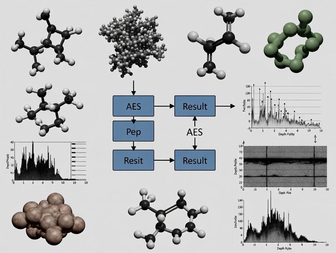
Visualization: AES Process and Analytical Workflow
Title: The Auger Electron Emission Process and Analysis Chain
Title: AES Protocol for Surface Contamination & Failure Analysis
The Scientist's Toolkit: Essential Research Reagent Solutions & Materials
Table 3: Key Materials for AES-Based Surface Analysis
| Item | Function/Application in AES |
|---|---|
| Conductive Adhesives (Carbon Tape, Silver Paint, Copper Tape) | Provides stable, electrical grounding of the sample to the holder to mitigate charging effects from the electron beam. Critical for insulating materials. |
| Standard Reference Materials (Pure Au, Ag, Cu foils, SiO₂/Si wafers) | Used for energy calibration of the spectrometer, verification of instrumental resolution, and checking relative sensitivity factors. |
| In-situ Sputter Ion Source (Argon Gas, ≥99.999% purity) | Provides controlled, in-situ surface cleaning to remove adventitious carbon/oxide layers and enables depth profiling by sequentially removing material. |
| Ultrasonic Cleaner & High-Purity Solvents (Isopropanol, Acetone, Methanol) | For ex-situ sample pre-cleaning to remove gross contaminants and salts prior to insertion into the ultra-high vacuum (UHV) system. |
| Specimen Stubs & Holders (Standard sizes for the instrument) | Mechanically secures the sample in the correct geometry for analysis. May include heating or cooling stages for in-situ studies. |
| Charge Neutralization System (Low-energy Electron Flood Gun or Ar⁺ Flood Source) | Essential for analyzing insulating samples (e.g., polymers, ceramics) by providing low-energy positive ions/electrons to compensate for surface positive charge buildup. |
Application Notes: Core Analytical Strengths in Failure Analysis
Auger Electron Spectroscopy (AES) provides unique capabilities for investigating surface contamination and material failures at the nanoscale, forming a critical thesis in modern analytical science. The following notes detail its principal advantages.
Table 1: Quantitative Comparison of AES with Competing Surface Techniques
| Feature / Parameter | AES | XPS (ESCA) | EDS (on SEM) | TOF-SIMS |
|---|---|---|---|---|
| Primary Information | Elemental (Z≥3) & Chemical State | Elemental (Z≥3) & Detailed Chemical State | Elemental (Z≥5) | Elemental & Molecular |
| Sampling Depth | 2-10 nm (5-10 Å escape depth) | 5-10 nm | 1-2 µm | 1-2 nm (top monolayer) |
| Lateral Resolution | < 10 nm (Field Emission) | 3-10 µm | 0.5-2 µm | 50-200 nm |
| Detection Limits (at.%) | 0.1 - 1% | 0.1 - 1% | 0.1 - 1% | ppm - ppb |
| Quantitative Accuracy | Good (±10-20%) with standards | Very Good (±5-10%) | Semi-Quantitative (±15-20%) | Poor (Requires standards) |
| Sputtering for Depth Profiling | Excellent: High-Speed, High-Resolution | Good | Poor | Good (Low Damage) |
| Sample Damage | Moderate (Electron Beam) | Very Low | Low | Very Low (Static) |
| Key Strength for Failure Analysis | High-Resolution 2D/3D Elemental Mapping & Interface Analysis | Chemical Bonding at Surfaces | Bulk Microanalysis | Ultra-Trace Surface Contamination |
Thesis Context: For research on electronic device failures or particulate contamination in pharmaceutical devices, AES’s combination of nanoscale lateral resolution and superb depth-profiling allows precise 3D reconstruction of contaminant layers, oxide films, and interfacial diffusion phenomena that are inaccessible to techniques with poorer spatial or depth resolution.
Experimental Protocols
Protocol 1: AES Depth Profiling of a Thin-Film Dielectric Failure
Objective: To determine the elemental composition and contamination depth distribution in a failed 50nm HfO₂ dielectric stack on a Si wafer.
Materials & Equipment:
- Field Emission Auger Electron Spectrometer (e.g., from Thermo Fisher, JEOL, or ULVAC-PHI)
- Argon ion sputtering gun (1-5 keV)
- Low-energy electron flood gun for charge neutralization (for insulating films)
- Standard reference materials (e.g., pure Cu, SiO₂)
- Conductive adhesive tape (e.g., carbon tape)
- Sample holders (stainless steel)
Procedure:
- Sample Preparation:
- Cleave the failed device to expose the region of interest (~5x5 mm).
- Mount using conductive tape on a standard holder. Ensure electrical contact.
- Optionally, mark the analysis area with a low-power optical microscope.
Instrument Setup:
- Insert sample into the analysis chamber. Achieve ultra-high vacuum (< 5 x 10⁻⁹ Torr).
- Align sample height to the spectrometer focal point.
- Set primary electron beam: 10 keV, 10 nA, beam diameter < 10 nm.
- Configure the cylindrical mirror analyzer (CMA) for a survey spectrum (e.g., 0-2000 eV with 1 eV step).
Initial Surface Analysis:
- Acquire a survey spectrum from the as-received surface at three representative points.
- Identify all elements present (C, O, Hf, Si, potential contaminants like Na, Cl, F).
- Perform high-resolution multiplex scans for key elemental peaks (e.g., C KLL, O KLL, Hf MNN) for chemical state information.
Sputter Depth Profiling:
- Program the sequential analysis cycle: a. Acquire Auger peak-to-peak heights (or area) for elements of interest (C, O, Hf, Si). b. Sputter the surface with a focused Ar⁺ ion beam (2 keV, 1x1 mm raster, calibrated sputter rate ~5 nm/min for SiO₂ equivalent). c. Repeat cycle.
- Use a low sputter rate initially to avoid interface mixing. Collect data until the Si substrate signal stabilizes.
Data Analysis:
- Convert sputter time to depth using the calibrated rate (confirmed via a SiO₂/Si standard).
- Plot atomic concentration (%) vs. depth (nm) using relative sensitivity factors (RSFs).
- Identify the interface width and correlate contaminant peaks (e.g., C) with failure locations.
Protocol 2: 2D Elemental Mapping of a Micron-Scale Contaminant Particle
Objective: To identify the elemental composition and distribution of an isolated particulate contaminant (~1µm) on a drug-eluting implant surface.
Procedure:
- Locate Particle:
- Transfer the sample to the AES stage.
- Use the instrument's secondary electron imaging (SEI) capability at low beam current to locate the particle without significant damage.
Mapping Acquisition:
- Define a raster area (e.g., 10x10 µm) encompassing the particle and surrounding substrate.
- Set the electron beam parameters: 10 keV, 1 nA (to reduce beam damage).
- For each pixel in the raster, acquire the Auger spectrum or set the CMA to sequentially detect specific elemental energies.
- Acquire maps for C KLL, O KLL, N KLL, and any suspected metal peaks (e.g., from processing tools: Fe, Cr, Ni).
- Acquisition time per map: typically 5-15 minutes, depending on signal-to-noise requirements.
Point Analysis:
- After mapping, perform a stationary point analysis on the center of the particle and on the clean substrate adjacent to it.
- Acquire high-resolution spectra for quantitative comparison.
Data Interpretation:
- Overlay elemental maps to assess co-localization.
- Compare spectra from the particle and substrate to confirm the exogenous nature of the contaminant.
Visualization: Experimental & Analytical Workflows
Diagram 1: AES Failure Analysis Decision Pathway
Title: AES Failure Analysis Decision Tree
Diagram 2: AES Instrumentation & Signal Generation Logic
Title: AES Signal Generation & Analysis Chain
The Scientist's Toolkit: Essential Research Reagents & Materials
Table 2: Key Reagent Solutions and Materials for AES Surface Analysis
| Item | Function / Purpose |
|---|---|
| Argon (Ar), 99.999% Pure | Inert sputtering gas for depth profiling and surface cleaning. High purity minimizes introduction of new contaminants. |
| Conductive Adhesives (Carbon Tape, Silver Paste) | To mount non-conductive or powder samples, providing a path for charge dissipation and stable grounding. |
| Standard Reference Materials (e.g., Pure Cu foil, SiO₂/Si wafer) | For quantitative calibration, sputter rate determination, and instrument performance verification. |
| In-Situ Cleaving Tool (for UHV chambers) | To expose a fresh, uncontaminated surface of brittle materials (semiconductors, oxides) inside the vacuum. |
| Low-Energy Electron Flood Gun Source | Provides low-energy electrons to neutralize surface charge on insulating samples, enabling accurate analysis. |
| HPLC-Grade Solvents (Isopropanol, Methanol) | For ultrasonic cleaning of sample holders and tools prior to introduction into the UHV chamber to reduce hydrocarbon background. |
| Calibrated Sputter Rate Standards (Ta₂O₅, SiO₂) | Thin films with known thickness used to calibrate ion sputter rates for accurate depth scale conversion. |
| Certified Particle/Density Standards (e.g., Polystyrene Latex Spheres) | For verifying the lateral resolution and magnification of the AES microprobe. |
Within the broader thesis on Auger Electron Spectroscopy (AES) for surface contamination and failure analysis in pharmaceutical and materials research, mastering three critical parameters—sampling depth, lateral resolution, and detection limits—is paramount. These parameters dictate the technique's efficacy in identifying nanoscale contaminants, mapping element distribution on device surfaces, and pinpointing the root cause of failures in drug delivery systems or microelectronic components. This application note provides a detailed protocol framework for researchers to optimize these parameters, ensuring reliable and interpretable data for critical quality attribute (CQA) assessment.
Core Parameter Definitions and Quantitative Data
Sampling Depth in AES is defined by the inelastic mean free path (IMFP) of Auger electrons, which is material- and energy-dependent. It typically ranges from 0.5 to 10 nm, making AES an ultra-surface-sensitive technique.
Lateral Resolution is determined by the diameter of the primary electron beam. State-of-the-art field emission AES systems can achieve resolutions below 10 nm.
Detection Limits vary by element and matrix but generally range from 0.1 to 1.0 atomic percent for most elements under optimal conditions.
Table 1: Summary of Critical AES Parameters for Common Applications
| Parameter | Typical Range | Key Influencing Factors | Impact on Failure Analysis |
|---|---|---|---|
| Sampling Depth | 0.5 – 10 nm | Auger electron kinetic energy, material density | Defines probed volume for contamination layers. |
| Lateral Resolution | 10 – 50 nm (FE sources) | Electron gun brightness, beam alignment, astigmatism | Determines smallest contaminant particle or feature that can be chemically identified. |
| Detection Limit | 0.1 – 1.0 at.% | Signal-to-noise ratio, background subtraction, peak overlap | Determines minimum concentration of a contaminant that can be reliably detected. |
| Analysis Area | ~1 µm² for point analysis | Beam diameter, scan coil settings | Must be optimized to target specific failure sites. |
Table 2: Inelastic Mean Free Path (IMFP, in nm) for Select Elements (Approx. 1000 eV)
| Matrix Material | C (272 eV) | O (503 eV) | Fe (703 eV) | Si (1619 eV) |
|---|---|---|---|---|
| Carbon | ~1.0 nm | ~1.5 nm | ~1.8 nm | ~2.8 nm |
| Silicon | ~0.9 nm | ~1.4 nm | ~1.7 nm | ~2.6 nm |
| Iron | ~0.7 nm | ~1.1 nm | ~1.4 nm | ~2.2 nm |
| Gold | ~0.6 nm | ~0.9 nm | ~1.1 nm | ~1.8 nm |
Experimental Protocols
Protocol 1: Determining Effective Sampling Depth via Angle-Resolved AES (AR-AES)
Objective: To experimentally determine the thickness of an ultra-thin oxide or contamination layer. Reagents/Materials: See "The Scientist's Toolkit" below. Method:
- Sample Mounting: Mount the sample on a stage capable of precise azimuthal rotation (tilt) relative to the analyzer.
- Initial Alignment: At 0° tilt (normal emission), locate the analysis area using secondary electron imaging.
- Data Acquisition: a. Acquire a survey spectrum (e.g., 0-1000 eV) to identify key substrate (e.g., Si) and overlayer (e.g., O, C) peaks. b. Set multiplex windows for the key substrate (e.g., Si LVV at 92 eV) and overlayer (e.g., O KLL at 503 eV) peaks. c. Acquire peak intensities while incrementally tilting the sample from 0° to 60° (e.g., in 10° steps). Note: Tilt increases the effective path length of electrons through the overlayer, enhancing surface sensitivity.
- Data Analysis: Plot the normalized substrate signal intensity (I/I₀) versus 1/cos(θ). The slope is related to the overlayer thickness via a simple exponential attenuation model.
Protocol 2: Optimizing Lateral Resolution for Contaminant Mapping
Objective: To achieve the highest spatial resolution for mapping elemental distribution of a particulate contaminant. Reagents/Materials: See "The Scientist's Toolkit" below. Method:
- Beam Alignment & Stigmation: a. Using a Faraday cup or a sharp, high-contrast feature on a calibration sample (e.g., Au on Si), focus the electron beam at the desired analysis energy (e.g., 10 keV). b. Adjust the stigmator coils to obtain a symmetrical, circular beam spot. This is critical for sub-50 nm resolution.
- Resolution Verification: Image a known nanostructure (e.g., a Ti/Pt test grid) and perform a line scan across a sharp edge. Measure the distance between 20% and 80% intensity points on the edge response function.
- Contaminant Analysis: a. Locate the contaminant particle or feature of interest using high-resolution SEM. b. Acquire a point spectrum on the particle and an adjacent "clean" area to identify differentiating elements. c. Set up elemental maps for these key elements (e.g., Na, Cl, Al) using the smallest practical beam current that provides acceptable count rates. d. Acquire maps with pixel density sufficient to resolve the feature (typically 256 x 256 pixels over the area of interest).
Protocol 3: Pushing Detection Limits for Trace Surface Contamination
Objective: To detect and quantify trace-level surface contaminants (e.g., <0.5 at.%). Reagents/Materials: See "The Scientist's Toolkit" below. Method:
- Spectrum Acquisition for Optimal SNR: a. Select a primary beam energy (Ep) that maximizes the Auger yield for the element of interest (typically 3-5 times the Auger transition energy). b. Use a low beam current to minimize sample damage, but increase dwell time per data point to improve statistics. c. Acquire a high-resolution multiplex spectrum over a narrow energy range containing the peak of interest and its background. Use a minimum of 0.1 eV/step.
- Background Subtraction & Peak Identification: a. Apply a Shirley or linear background subtraction to the raw spectrum. b. Identify the peak position and measure the peak-to-peak height (in derivative mode) or integrated area (in direct N(E) mode).
- Quantification: a. Compare the measured peak intensity to sensitivity factors derived from standard samples. b. Report detection limits based on a signal-to-noise ratio (SNR) > 3. The noise is typically measured as the root-mean-square variation in the background.
Visualizations
Diagram Title: AES Parameter Optimization Workflow
Diagram Title: Sampling Depth & Signal Attenuation in AES
The Scientist's Toolkit: Essential Research Reagent Solutions
Table 3: Key Materials and Reagents for AES Surface Analysis
| Item | Function in AES Protocols | Example/Notes |
|---|---|---|
| Conductive Tape/Adhesive | Provides electrical and mechanical grounding of insulating samples to prevent charging. | Carbon tape, silver paste, or copper tape. |
| Reference Calibration Samples | For verifying lateral resolution, energy calibration, and sensitivity factors. | Au grid on Si, pure elemental foils (e.g., Cu, Al, Ag). |
| Argon Gas (Ultra-High Purity) | Source for ion sputtering guns used for depth profiling and surface cleaning. | 99.999% purity to minimize implantation of reactive gases. |
| Standard Reference Materials (SRMs) | Thin film standards with known composition/thickness for quantitative accuracy. | NIST-certified SiO₂ on Si, multi-layer metal films. |
| Charge Neutralization Source | Low-energy electron or ion flood gun for analyzing insulating samples (e.g., drug particles). | Essential for pharmaceuticals and polymers. |
| Ultrasonic Solvent Cleaner | For preliminary sample cleaning in solvents (acetone, ethanol, IPA) to remove gross contamination. | Must be followed by in-situ cleaning (sputtering) for valid analysis. |
| Handling Tools (Tweezers, Gloves) | For contamination-free sample transfer and mounting. | Anti-magnetic, non-particulating tweezers; powder-free nitrile gloves. |
This application note is framed within a broader thesis that asserts Auger Electron Spectroscopy (AES) is a critical, high-sensitivity surface analysis technique for root-cause investigation in pharmaceutical development and manufacturing. The core thesis is that AES provides unparalleled spatial resolution (down to ~10 nm) and elemental sensitivity (typically 0.1-1 at.%) for mapping surface chemistry, making it indispensable for solving problems related to invisible contaminants, thin-film coating integrity, and material interactions that directly impact drug safety, efficacy, and stability.
Application Note: Identification of Inorganic Contaminants on Tablet Surfaces
Problem: Discoloration spots observed on compressed tablet cores prior to coating. Energy-Dispersive X-Ray Spectroscopy (EDS) detected only trace levels of silicon and aluminum, insufficient for definitive identification.
AES Protocol & Results:
- Sample Preparation: A tablet with a visible spot was carefully fractured in a laminar flow hood to expose the sub-surface region near the discoloration. A cross-section was mounted on an AES sample holder using conductive carbon tape.
- Instrument Parameters:
- Instrument: Field Emission-Auger Electron Spectrometer.
- Primary Beam Energy: 10 keV.
- Beam Current: 10 nA.
- Analysis Mode: Secondary Electron Imaging (SEI) for localization, followed by point analysis and elemental mapping.
- Analysis Workflow: a. SEI identified a ~5 µm particulate at the center of the discoloration. b. High-resolution point AES spectrum acquired from the particle. c. Elemental mapping performed for C, O, Al, Si, and Mg over a 20x20 µm area.
- Data Interpretation: The point spectrum showed intense Al and Si peaks with minor Mg. The map revealed a correlated Al-Si-Mg signal localized to the particle, surrounded by a carbon/oxygen matrix (excipients). Quantitative analysis confirmed a silicate-based contaminant (e.g., kaolin or clay).
Table 1: Quantitative AES Analysis of Tablet Contaminant
| Element | Atomic % (Particle) | Atomic % (Clean Bulk) | Likely Origin |
|---|---|---|---|
| O | 62.1 | 22.3 | Silicate, Excipients |
| C | 5.8 | 71.5 | Organic Excipients |
| Si | 18.4 | 0.2 | Contaminant (Clay) |
| Al | 12.5 | 0.0 | Contaminant (Clay) |
| Mg | 1.2 | 0.0 | Contaminant (Clay) |
Note: Balance includes trace Na, Ca.
Application Note: Failure Analysis of a Pinhole Defect in a Controlled-Release Film Coating
Problem: Pinhole defects in a polymer-based controlled-release coating lead to premature drug release (dose dumping). Optical and scanning electron microscopy (SEM) revealed the defect morphology but not the chemical cause.
AES Protocol & Results:
- Sample Preparation: A coated tablet with a identified pinhole was cross-sectioned using a focused ion beam (FIB) mill to create a pristine, contamination-free vertical slice through the pinhole defect. This preserves the interface chemistry for analysis.
- Instrument Parameters:
- Primary Beam Energy: 15 keV (for high spatial resolution mapping).
- Beam Current: 1 nA.
- Analysis Mode: AES line scan and depth profiling across the pinhole wall.
- Analysis Workflow: a. SEI located the FIB-cut cross-section of the pinhole. b. A line scan (50 points, 10 nm step) was performed from the intact coating, across the pinhole edge, to the tablet core. c. A depth profile (sputtering with 1 keV Ar⁺ ions) was performed at the pinhole edge to examine interfacial layers.
- Data Interpretation: The line scan showed a sudden loss of polymer-specific elements (C, O) and a coincident spike in magnesium stearate at the pinhole boundary. Depth profiling confirmed a ~50 nm thick layer of magnesium stearate (lubricant) embedded at the coating-substrate interface, acting as a dewetting site and causing coating failure.
Table 2: AES Depth Profile at Pinhole Interface (First 3 Minutes Sputtering)
| Sputter Time (min) | Atomic % C | Atomic % O | Atomic % Mg | Atomic % P (API) | Interpreted Layer |
|---|---|---|---|---|---|
| 0.0 | 78.5 | 21.2 | 0.3 | 0.0 | Polymer Coating |
| 0.5 | 72.1 | 18.5 | 9.4 | 0.0 | Mg Stearate Rich |
| 1.0 | 65.8 | 15.2 | 18.9 | 0.1 | Mg Stearate Rich |
| 2.0 | 10.5 | 58.3 | 1.2 | 30.0 | API Layer |
Experimental Protocols
Protocol 1: AES Analysis of Particulate Contaminants on Medical Devices
- Isolation: Use micro-manipulators or adhesive carbon tabs in a clean bench to transfer the particulate to a clean, polished silicon wafer.
- Mounting: Secure the wafer to the AES sample holder with a metal clamp.
- Charge Neutralization: For insulating particles, use a low-energy (~1 eV) electron flood gun. Optimize flux to stabilize the AES signal without degrading the sample.
- Screening: Acquire a survey spectrum from 20-1200 eV at the particle.
- High-Resolution Mapping: For key elements (e.g., Cl, S, F, metals), acquire high-count maps with a step size ≤50 nm to define morphology.
- Quantification: Use instrument sensitivity factors and a standardless routine, but corroborate with a known standard (e.g., pure Cu foil) if absolute accuracy is critical.
Protocol 2: AES Depth Profiling for Interface Failure in Multi-Layer Tablets
- Cross-Section Prep: Critical Step. Use FIB milling to prepare a trench with a smooth, vertical wall exposing all layers. Avoid smearing with a protective Pt/Pd deposition layer.
- Align Sample: Tilt the sample so the analysis surface is normal to the electron beam. Pre-sputter the area with a broad, low-energy Ar⁺ beam to remove ambient contamination.
- Define Profile Parameters: Set a rastered ion beam (1-3 keV Ar⁺) over an area ~50% larger than the analysis area. Use an electron beam for analysis in the center of the sputtered crater.
- Acquisition: Cycle between short sputter intervals (e.g., 5-15 seconds) and AES survey/high-resolution scans for key elements. Continuously monitor peak shapes for chemical state changes.
- Data Reduction: Plot atomic concentration vs. sputter time/depth. Identify interfaces where significant concentration gradients occur (>50% change over <5 nm is indicative of a sharp interface).
Visualizations
AES Surface Failure Analysis Workflow
AES vs EDX Signal Generation Depth
The Scientist's Toolkit: Key Research Reagent Solutions
| Item/Reagent | Function in AES Pharma Analysis | Critical Specification |
|---|---|---|
| Polished Silicon Wafers | Ideal, ultra-clean substrate for mounting and analyzing particulate contaminants. Low background AES signal. | Prime grade, 99.999% pure, native oxide layer acceptable. |
| Conductive Carbon Tabs/Dots | For mounting insulating samples (tablet fragments, powders) to minimize charging. | High-purity, adhesive, compatible with ultra-high vacuum (UHV). |
| FIB Lift-Out Kit (Pt/Ga sources) | For preparing site-specific cross-sections of coating defects or interfaces. | Electron beam- and ion beam-deposited precursor gases (e.g., Pt, W). |
| Argon Gas (Research Grade) | Sputtering gas for depth profiling and surface cleaning. Must be ultra-pure to avoid implantation artifacts. | 99.9999% purity, with integrated gas purifier/filter. |
| Standard Reference Materials | For quantitative calibration and instrument performance verification (e.g., pure Cu, Au, SiO₂). | Certified, clean, and stable under electron beam. |
| Micro-manipulators & Probes | For the precise isolation and transfer of microscopic contaminants under optical control. | Tungsten or stainless steel tips, vibration-isolated stage. |
Within the context of advancing surface contamination and failure analysis research, Auger Electron Spectroscopy (AES) remains a critical technique for elemental and chemical-state characterization of solid surfaces. This application note details the core components of a modern AES system, providing protocols and resources tailored for researchers and drug development professionals focused on particulate contamination, thin-film delamination, and corrosion analysis in biomedical devices and pharmaceutical manufacturing.
Core Instrumentation Components
Electron Optics Column
The electron gun and focusing lenses are fundamental for generating a stable, high-brightness primary electron beam. Modern systems utilize field emission guns (FEG) for superior spatial resolution (<10 nm). The column includes electrostatic or electromagnetic lenses for beam focusing and scanning coils for rastering the beam across the sample surface.
Electron Energy Analyzer
The heart of the AES system, typically a hemispherical sector analyzer (HSA) or cylindrical mirror analyzer (CMA). It disperses emitted electrons based on kinetic energy, providing the high energy resolution necessary for chemical state identification.
Ultra-High Vacuum (UHV) Chamber
Essential for maintaining surface cleanliness and enabling the detection of low-energy Auger electrons without gas-phase scattering. Base pressures typically range from 10⁻⁸ to 10⁻¹⁰ Pa.
Sample Handling and Stage
A precision, multi-axis manipulator that allows for heating, cooling (often from -120°C to 1000°C), and tilt/rotation for depth profiling and angle-resolved measurements.
Sputter Ion Gun
A focused ion source (usually Ar⁺) for depth profiling by controlled surface erosion and for in-situ cleaning of sample surfaces.
Detection System
An electron multiplier or channel electron multiplier array that converts the energy-resolved electron current into an amplified signal for processing.
Data Acquisition and Control System
Computer-controlled software for instrument operation, spectral acquisition, data processing (including differentiation, background subtraction, and peak fitting), and elemental mapping.
Quantitative Performance Data
Table 1: Performance Specifications of Modern AES Components
| Component | Key Parameter | Typical Specification Range | Impact on Analysis |
|---|---|---|---|
| Electron Gun | Beam Energy | 1 keV to 30 keV | Controls sampling depth & excitation efficiency |
| Beam Current | 100 pA to 1 µA | Affects spatial resolution & signal-to-noise | |
| Probe Size (FEG) | 5 - 20 nm | Determines ultimate spatial resolution | |
| Energy Analyzer | Energy Resolution (ΔE/E) | 0.05% - 0.6% | Dictates peak separation & chemical state ID |
| Constant Pass Energy | 10 - 200 eV | Balances resolution & transmission | |
| Ion Gun | Sputter Rate (SiO₂) | 0.1 - 10 nm/min | Controls depth profiling speed & resolution |
| Beam Energy (Ar⁺) | 0.5 - 5 keV | Affects depth resolution & sample damage | |
| Detection Limit | Atomic Concentration | 0.1 - 1.0 at.% | Minimum detectable elemental concentration |
| Lateral Resolution | X-Y Mapping | < 10 nm (FEG systems) | Detail in contamination mapping |
Experimental Protocols
Protocol 1: AES Point Analysis for Surface Contamination Identification
Objective: To identify unknown particulate or thin-film contamination on a device surface. Materials: Sample, conductive adhesive (if insulating), standard reference materials (e.g., pure Cu, Si). Procedure:
- Sample Mounting: Secure sample on holder using clips or conductive tape. Ensure electrical contact for charge compensation if non-conductive.
- Load & Pump: Insert into UHV load lock, pump to <10⁻⁵ Pa, then transfer to analysis chamber (<10⁻⁸ Pa).
- Locate Feature: Use integrated SEM or optical microscope to navigate to the feature of interest.
- Optimize Beam: Set primary beam energy (typically 10 keV for survey, 5-10 keV for high-resolution). Adjust beam current to 1-10 nA for point analysis.
- Acquire Survey Spectrum: Set analyzer to constant retard ratio (e.g., 4) or constant pass energy (e.g., 100 eV). Acquire spectrum from 30 eV to 2000 eV.
- Identify Elements: Differentiate spectrum (dN(E)/dE) to enhance Auger peaks. Identify all elements present from peak positions.
- High-Resolution Scan: For key elements (e.g., C, O, N), acquire narrow scans over relevant energy windows with higher energy resolution (e.g., 20 eV pass energy, 0.1 eV/step).
- Data Analysis: Compare peak shapes and energies to standard spectral libraries to infer chemical states (e.g., carbide vs. graphitic carbon).
Protocol 2: AES Depth Profiling for Thin-Film Failure Analysis
Objective: To determine the elemental composition as a function of depth at a site of interfacial failure (e.g., delamination). Materials: Sample, argon gas supply (99.999% purity). Procedure:
- Initial Surface Analysis: Perform Protocol 1, Step 5-7 at the analysis site.
- Select Sputter Parameters: Define a sputter crater larger than the analysis area. Typical settings: 1-4 keV Ar⁺, beam current density 10-50 µA/cm², raster over 2x2 mm area.
- Set Profiling Sequence: Program an alternating cycle of: a. Sputter Etch: Apply ion beam for a time calculated to remove ~1-5 nm per cycle (calibrated on a standard like Ta₂O₅). b. Analysis: Move sample to center of crater. Acquire spectra for major element peaks identified in the survey. Use same analyzer settings for each cycle.
- Execute Profile: Run automated sequence for 50-200 cycles, depending on desired depth.
- Data Quantification: Use relative sensitivity factors (RSFs) to convert peak-to-peak heights in differentiated spectra to atomic concentrations for each element at each cycle.
- Depth Calibration: Convert cycle number to depth (nm) using known sputter rate for a standard or by measuring final crater depth with a profilometer.
Visualizations
Diagram 1: AES System Workflow
Diagram 2: AES Signal Acquisition Logic
The Scientist's Toolkit: Research Reagent Solutions
Table 2: Essential Materials for AES-Based Contamination Analysis
| Item | Function & Application | Key Consideration |
|---|---|---|
| Conductive Adhesive Tapes/Carbon Paints | Mounting insulating samples to prevent charging. | Low outgassing in UHV; minimal contaminant background (low Na, K, Cl). |
| Argon Gas (99.999%+) | Source gas for sputter ion gun for depth profiling and cleaning. | High purity critical to avoid implanting reactive contaminants (e.g., O₂, H₂O). |
| Standard Reference Materials (NIST-traceable) | Quantification calibration (e.g., pure Cu, Au, Si) and sputter rate calibration (e.g., Ta₂O₅, SiO₂/Si). | Certified composition and known, stable oxide thickness. |
| Charge Neutralization Source (Flood Gun) | Low-energy electron/ion beam for stabilizing potential on insulators. | Essential for analyzing polymers or ceramic contaminants. |
| In-situ Cleaving/Fracture Stage | Creates clean, fresh surfaces within UHV for analyzing bulk composition or grain boundary chemistry. | Used in failure analysis of brittle fractures. |
| UHV-Compatible Solvents (e.g., HPLC-grade Isopropanol) | For pre-cleaning samples in a controlled manner before insertion to reduce hydrocarbon load. | Minimizes adventitious carbon layer, reducing analysis time. |
Practical AES Workflows: From Sample Prep to Data Interpretation in Drug Development
Article Context
This application note, framed within a broader thesis on Auger Electron Spectroscopy (AES) for surface contamination and failure analysis research, details a comprehensive protocol for conducting a complete AES investigation. It provides researchers, scientists, and drug development professionals with a standardized methodology for identifying elemental surface composition, mapping spatial distribution, and obtaining quantitative depth profiles, which is critical for root-cause analysis in device failures, coating integrity assessment, and contamination studies in pharmaceutical manufacturing.
Auger Electron Spectroscopy is a surface-sensitive analytical technique used to determine the elemental composition (for elements Z > 2) of the top 0.5-10 nm of a solid surface. The core workflow involves three sequential phases: Spectral Acquisition for qualitative and quantitative analysis, Elemental Mapping for spatial distribution, and Sputter Depth Profiling for compositional analysis as a function of depth.
Detailed Experimental Protocols
Objective: To introduce a contamination-free, electrically stabilized sample into the ultra-high vacuum (UHV) analysis chamber. Materials: Conductive adhesive tape (e.g., carbon tape), ultrasonic cleaner, high-purity solvents (isopropanol, acetone), inert gas duster, standard sample holder. Procedure:
- Cleaning: For non-delicate samples, perform sequential ultrasonic cleaning in acetone and isopropanol for 5 minutes each. Dry with a stream of dry, oil-free nitrogen gas.
- Mounting: For electrically insulating samples, apply a strip of conductive carbon tape to the sample holder and affix the sample. Ensure a secure mechanical and electrical connection to minimize charging.
- Introduction: Transfer the mounted sample to the UHV introduction chamber. Pump down to a pressure of ≤ 1 x 10⁻⁶ mbar.
- Transfer: Open the gate valve and transfer the sample to the analysis chamber (pressure ≤ 5 x 10⁻⁹ mbar). Allow thermal equilibration for 15-30 minutes.
Protocol 2.2: Spectral Acquisition and Qualitative Analysis
Objective: To acquire a survey spectrum from a point on the sample to identify all detectable elements present. Instrument Parameters (Typical):
- Primary Electron Beam: 10 keV, 10 nA beam current.
- Beam Diameter: ~100 nm (dependent on instrument).
- Analysis Area: Typically 1 x 1 µm² to 10 x 10 µm².
- Detector: Cylindrical Mirror Analyzer (CMA). Set pass energy to 100 eV for survey scans, 20-50 eV for high-resolution multiplex scans. Procedure:
- Region Selection: Using the microscope, navigate to a representative area of interest on the sample.
- Beam Alignment: Optimize the electron gun alignment and adjust the sample's Z-position (working distance) for maximum signal.
- Survey Scan Acquisition: Acquire a spectrum over a kinetic energy range of 30 eV to 2000 eV. Use an energy step size of 0.5-1 eV and a dwell time of 50-100 ms per point.
- Peak Identification: Process the spectrum by applying a smoothing function (e.g., Savitzky-Golay) and a linear or Shirley background subtraction. Identify all major and minor Auger peaks by matching their kinetic energies to standard reference databases.
- Multiplex Scan: For quantitative analysis, acquire high-resolution scans over the energy range of each identified elemental peak (e.g., C KLL, O KLL, Fe LMM). Use a pass energy of 20-50 eV.
Protocol 2.3: Quantitative Analysis (Sensitivity Factor Method)
Objective: To convert measured peak intensities into atomic concentrations. Procedure:
- Peak Intensity Measurement: For each element identified, measure the peak-to-peak height (in derivative dN(E)/dE mode) or the integrated area under the peak (in direct N(E) mode after background subtraction) from the high-resolution multiplex scan.
- Apply Relative Sensitivity Factors (RSFs): Calculate atomic concentration using the formula: [ Cx = \frac{Ix / Sx}{\sum{i} (Ii / Si)} ] where (Cx) is the atomic concentration of element (x), (Ix) is the measured peak intensity, and (S_x) is the relative sensitivity factor for that element under the specific instrument conditions. RSFs are typically provided by the instrument manufacturer or derived from standard samples.
Table 1: Example Quantitative AES Data from a Contaminated Silicon Wafer
| Element | Peak Energy (eV) | Peak Intensity (a.u.) | RSF (Provided) | Atomic Concentration (%) |
|---|---|---|---|---|
| C (KLL) | 272 | 125,400 | 0.18 | 32.5% |
| O (KLL) | 503 | 89,200 | 0.34 | 12.3% |
| Si (KLL) | 1619 | 305,000 | 0.32 | 45.2% |
| Fe (LMM) | 703 | 12,500 | 0.25 | 2.3% |
| Na (KLL) | 990 | 8,750 | 0.15 | 2.7% |
Protocol 2.4: Elemental Mapping
Objective: To visualize the two-dimensional spatial distribution of elements on the sample surface. Procedure:
- Parameter Setup: Define the analysis area (e.g., 50 x 50 µm²). Set the electron beam parameters (e.g., 10 keV, 10 nA).
- Peak and Background Selection: For each element of interest, select the kinetic energy window for the peak (P) and two background windows (B1, B2) on either side of the peak.
- Scan Acquisition: Raster the focused electron beam over the defined area. At each pixel, the analyzer sequentially acquires counts at the peak and background energies. The net signal is calculated as (P - (B1+B2)/2).
- Image Generation: Construct a 2D map where the pixel intensity is proportional to the net Auger signal for the selected element.
- Overlay: Create composite overlay maps to show co-localization of different elements.
Protocol 2.5: Sputter Depth Profiling
Objective: To determine the in-depth elemental composition of thin films or contamination layers. Procedure:
- Initial Surface Analysis: Acquire a survey spectrum from the analysis point.
- Sputter Source Setup: Use an inert gas ion gun (typically Ar⁺) with an acceleration voltage of 0.5 - 5 keV and a rastered beam over an area larger than the analysis area to ensure a flat-bottomed crater.
- Cyclic Data Acquisition: A single profile cycle consists of: a. Sputtering: Erode the surface for a fixed time interval (e.g., 5-30 seconds), defining the depth resolution. b. Analysis: Acquire multiplex spectra for all elements of interest from the central, flat portion of the crater.
- Repetition: Repeat the sputter-analysis cycle until the substrate or a layer of interest is fully exposed.
- Depth Calibration: Convert sputter time to depth by measuring the total crater depth post-analysis using a stylus profilometer and assuming a constant sputter rate. Sputter rates are material-dependent.
Table 2: Sputter Depth Profiling Parameters for a 100 nm TiN Coating
| Parameter | Setting 1 (High Res) | Setting 2 (Through Layer) |
|---|---|---|
| Ion Species | Ar⁺ | Ar⁺ |
| Ion Energy | 1 keV | 3 keV |
| Ion Current Density | 0.5 µA/cm² | 2 µA/cm² |
| Raster Area | 2 x 2 mm² | 2 x 2 mm² |
| Analysis Area | 100 x 100 µm² | 100 x 100 µm² |
| Cycle Time (Sputter + Analyze) | 20 s | 15 s |
| Estimated Depth Resolution (at interface) | ~3 nm | ~8 nm |
The Scientist's Toolkit: Essential Research Reagent Solutions
Table 3: Key Reagents and Materials for AES Sample Preparation and Analysis
| Item | Function/Benefit |
|---|---|
| High-Purity Solvents (HPLC Grade Acetone & Isopropanol) | Removes organic contaminants and particles from sample surfaces without leaving significant residues. |
| Conductive Carbon Tape | Provides a reliable, low-outgassing method for mounting and electrically grounding non-conductive or irregularly shaped samples. |
| Dry, Oil-Free Nitrogen Gas | Provides a clean, non-contaminating method for drying solvents from sample surfaces after cleaning. |
| Argon Gas (99.9999% purity) | Source gas for the ion gun used in sputter cleaning and depth profiling. High purity minimizes introduction of new contaminants. |
| Standard Reference Materials (e.g., Pure Cu, Au, Si) | Used for instrumental energy calibration, verifying resolution, and determining relative sensitivity factors (RSFs) for quantification. |
| Cleaned, Polished Stainless Steel or Mo Sample Holders | Provide a uniform, low-outgassing, and electrically conductive platform for mounting samples in the UHV system. |
Visualized Workflows and Relationships
Title: Comprehensive AES Analysis Workflow Diagram
Title: AES Signal Generation and Detection Pathway
1.0 Introduction
Within the broader thesis on the application of Auger Electron Spectroscopy (AES) for surface contamination and failure analysis, this case study exemplifies its critical role in medical device diagnostics. Inorganic surface contaminants, such as salts, residual processing chemicals, and particulate matter, can compromise device performance, lead to adverse biological reactions, and cause product failure. AES provides unparalleled sensitivity for light elements and offers high spatial resolution (<10 nm), enabling the precise localization and chemical state identification of inorganic residues at the outermost surface layers (1-5 nm), which are often undetectable by bulk techniques.
2.0 Key Contaminants & Data Summary
The following table summarizes common inorganic contaminants identified on medical device surfaces via AES, their potential sources, and associated risks.
Table 1: Common Inorganic Contaminants on Medical Devices
| Contaminant | Chemical Species | Potential Source | Identified Risk/Effect |
|---|---|---|---|
| Chlorides | NaCl, KCl, MgCl₂ | Fingerprints, saline solutions, process water | Pitting corrosion on stainless steel alloys, altered surface energy. |
| Sulfates | (NH₄)₂SO₄, CaSO₄ | Cleaning agents, water, environmental exposure | Can act as stress corrosion cracking initiators. |
| Silicates | SiO₂, Siloxanes | Molding release agents, dust, glassware | Insulating layers, poor adhesion of coatings, inflammatory response. |
| Phosphates | PO₄³⁻ compounds | Biologic residues, cleaning detergents | May interfere with intended bioactive surface modifications. |
| Calcium Salts | CaCO₃, Ca₃(PO₄)₂ | Hard water, biologic fluids | Occlusion of micro-fluidic channels, nucleation site for biofilms. |
| Transition Metals | Fe, Ni, Cr particles | Tooling wear, manufacturing debris | Catalytic degradation of polymers, cytotoxic effects. |
3.0 Experimental Protocols
3.1 Protocol for AES Analysis of a Coronary Stent Surface
- Objective: To map the distribution and identify the composition of particulate contamination on a laser-cut stainless steel coronary stent.
- Sample Preparation:
- Use conductive carbon tape to mount the stent to an AES sample holder.
- If the stent is non-conductive (e.g., polymer-coated), employ a low-voltage, short-duration carbon coating to prevent charging, ensuring it does not obscure surface contaminants.
- Handle all samples with powder-free nitrile gloves and ceramic tweezers to prevent additional contamination.
- AES Instrument Parameters (Typical):
- Primary Electron Beam: 10 keV, 10 nA.
- Beam Diameter: ~20 nm for point analysis; raster for mapping.
- Analysis Chamber Pressure: < 5 x 10⁻⁹ Torr.
- Sputtering Ion Gun (for depth profiling): Ar⁺, 1-3 keV, raster over 2x2 mm area.
- Procedure:
- Survey Scan: Acquire a wide energy survey spectrum (0-1000 eV) from multiple visually identified points of interest (clean area and particulate spots).
- High-Resolution Multiplex Scan: Perform narrow window scans on key elemental peaks (e.g., O KLL, C KLL, Cl LMM, Si KLL, Na KLL, Ca LMM) to determine chemical states.
- Elemental Mapping: Set the cylindrical mirror analyzer (CMA) to the kinetic energy of a specific Auger transition (e.g., Cl 181 eV). Raster the electron beam to create a 2D map of chlorine distribution.
- Depth Profiling: On a contaminated spot, alternately sputter the surface with the Ar⁺ ion gun and acquire AES spectra to determine the in-depth distribution of the contaminant layer.
- Data Interpretation: Compare the peak energies and line shapes from contaminant regions with reference spectra from known salts. Quantification using relative sensitivity factors (RSFs) provides atomic concentrations.
3.2 Protocol for Contaminant Removal Efficiency Validation
- Objective: To assess the efficacy of a new plasma cleaning process in removing residual silicate mold release agent from a polymer catheter hub.
- Procedure:
- Select 10 devices: 5 as-cleaned with the standard method, 5 cleaned with the new plasma method.
- Perform AES survey scans on an identical location (e.g., inner rim) on each device.
- Measure the intensity (peak-to-peak height in the derivative spectrum) of the Si KLL (1619 eV) signal.
- Normalize the Si signal to the dominant C KLL (272 eV) signal for each spectrum to account for slight topographic variations.
- Data Presentation: Report the mean normalized Si intensity and standard deviation for each batch. A statistical t-test confirms the significance of the reduction.
Table 2: AES Results for Cleaning Validation (Hypothetical Data)
| Cleaning Method | Mean Normalized Si Signal (a.u.) | Standard Deviation | Atomic % Si (Estimated) |
|---|---|---|---|
| Standard Wash | 0.85 | 0.15 | 12.5% |
| New Plasma Process | 0.04 | 0.02 | 0.6% |
4.0 Visualization: AES Failure Analysis Workflow
AES Failure Analysis Workflow
5.0 The Scientist's Toolkit: Research Reagent Solutions & Materials
Table 3: Essential Materials for AES-Based Contaminant Analysis
| Item | Function/Application |
|---|---|
| Conductive Carbon Tape/Dots | Provides electrical and thermal contact between sample and holder, preventing charging under electron beam. |
| Argon Gas (99.999% purity) | Source gas for the ion sputtering gun used for depth profiling and cleaning analysis areas. |
| Standard Reference Materials (e.g., SiO₂, NaCl wafer) | Used for instrument calibration, verification of energy scale, and confirming sensitivity factors. |
| High-Purity Solvents (IPA, Acetone) | For ultrasonic cleaning of sample holders and tools to prevent cross-contamination. |
| Ceramic or Non-Metallic Tweezers | To handle samples without transferring metallic ions or particles to critical surfaces. |
| Particle-Free Gloves (Nitrite) | Essential for sample preparation to avoid contamination from skin oils and salts (Na, K, Cl). |
| Gold or Carbon Sputter Coater | For applying a thin, conductive layer on insulating samples to facilitate AES analysis. |
This application note presents a systematic failure analysis protocol for delaminated drug-eluting coatings (DECs), framed within a broader thesis on the application of Auger Electron Spectroscopy (AES) for surface contamination and interfacial failure research. DELAMINATION is a critical failure mode in biomedical implants (e.g., stents, orthopedic devices) and can lead to loss of therapeutic efficacy, adverse biological responses, and device malfunction. AES provides nanoscale elemental mapping and depth profiling essential for identifying sub-micrometer contaminants, interfacial chemistry, and bonding failures invisible to optical or electron microscopy alone.
Based on current literature and failure analyses, primary mechanisms for DEC delamination are summarized in Table 1.
Table 1: Primary Mechanisms and Contributing Factors for DEC Delamination
| Mechanism | Description | Typical AES Findings | Frequency in Studies* (%) |
|---|---|---|---|
| Adhesive Failure | Separation at the coating-substrate interface. | Detection of interfacial contaminants (C, O, Si, S), absence of substrate elements (e.g., Co, Cr, Ti) in coating underside. | 45-60% |
| Cohesive Failure | Fracture within the coating polymer matrix itself. | Uniform elemental composition on both fracture faces; may show phase separation or filler agglomeration. | 20-30% |
| Hydrolitic Degradation | Polymer bond cleavage due to moisture ingress. | Increased oxygen at interface; possible correlation with coating thickness and porosity. | 10-20% |
| Stress-Induced Failure | Mismatch in thermal expansion or residual stress. | Clean interface in AES; failure correlates with mechanical testing data (e.g., adhesion pull-off). | 5-15% |
*Frequency data aggregated from recent studies (2020-2024).
Table 2: Common Interfacial Contaminants Identified by AES in Delaminated DECs
| Contaminant Element | Probable Source | Impact on Adhesion |
|---|---|---|
| Silicon (Si) | Silicone release agents, dust, process residues. | Severe reduction; forms weak boundary layer. |
| Sulfur (S) | Antioxidants, processing aids, or environmental exposure. | Moderate to severe reduction. |
| Chlorine (Cl) | Saline processing, residual solvents. | Promotes corrosive undercutting and adhesion loss. |
| Alkali Metals (Na, K) | Handling contaminants, biological fluids. | Catalyzes polymer degradation, reduces interfacial strength. |
Experimental Protocols
Protocol 1: AES-Based Failure Interface Analysis
Objective: To perform chemical characterization of both fracture surfaces (coating side and substrate side) of a delaminated DEC to determine failure mode.
Materials: See "The Scientist's Toolkit" below.
Method:
- Sample Preparation:
- Carefully separate delaminated fragments using ceramic tweezers.
- Mount each fragment (coating underside and substrate topside) on a conductive carbon tab or holder. Ensure electrical contact for charge compensation.
- Sputter-clean a small, non-critical area with a low-energy (500 eV, 1 µA) Ar⁺ ion beam for 30 seconds to remove adventitious carbon.
- AES Survey Scan:
- Operate AES system with a base pressure < 5 x 10⁻¹⁰ Torr.
- Set primary electron beam: 10 keV, 10 nA, spot size ~20 nm.
- Acquire survey spectra (0-1000 eV) from a minimum of 5 distinct points on each fracture surface.
- Identify all elements present (excluding Ar from sputtering).
- High-Resolution Mapping & Point Analysis:
- For elements of interest (e.g., C, O, N, substrate metals, contaminants), acquire high-resolution multiplex spectra.
- Perform elemental mapping (e.g., for Si, S, Cl) over a 20 µm x 20 µm area to visualize contaminant distribution.
- Depth Profiling (If Interface is Accessible):
- On a partially delaminated edge, perform AES depth profiling using a sequenced Ar⁺ sputter (2 keV, 2 µA, rastered).
- Monitor key element signals versus sputter time to reconstruct the interfacial chemistry.
Protocol 2: Correlative Microscopy Workflow for Root-Cause Analysis
Objective: To integrate AES data with structural and compositional data from other techniques for comprehensive root-cause determination.
Method:
- Initial Inspection: Use optical microscopy and scanning electron microscopy (SEM) to document delamination morphology and locate representative areas for analysis.
- Focused Ion Beam (FIB) Cross-Sectioning:
- At the delamination front, deposit a protective Pt strap.
- Mill a trench to create a thin electron-transparent lamella (~100 nm thick) perpendicular to the interface using Ga⁺ ions (30 keV then 5 keV for cleaning).
- Transmission Electron Microscopy (TEM) & EDS: Analyze the lamella via TEM for crystallographic and morphological defects. Perform energy-dispersive X-ray spectroscopy (EDS) for elemental composition.
- Targeted AES: Transfer the bulk sample (not the lamella) to the AES system. Use SEM images as a map to navigate to the exact region adjacent to the FIB site for AES point analysis as per Protocol 1.
- Data Correlation: Overlay AES contaminant maps with SEM/EDS data to identify if contaminants originate from the substrate, coating, or external environment.
Visualization of Analysis Workflow
Diagram Title: DEC Delamination Failure Analysis Decision Workflow
Diagram Title: Correlative Microscopy for DEC Failure Analysis
The Scientist's Toolkit: Key Research Reagent Solutions & Materials
Table 3: Essential Materials for AES-Based DEC Failure Analysis
| Item | Function in Analysis | Key Considerations |
|---|---|---|
| Conductive Carbon Tape/Dots | Mounting fragile delaminated fragments for SEM/AES. | Must be ultra-high purity to avoid introducing Si, S, or Cl contaminants detectable by AES. |
| Ceramic-Coated Tweezers | Handling samples to prevent introduction of metallic contamination. | Prevents false-positive detection of Fe, Ni, Cr from stainless steel tweezers. |
| Argon (Ar), 99.9999% | Gas for ion sputter cleaning and depth profiling in AES. | High purity is critical to avoid implanting residual gas contaminants (e.g., H₂O, N₂) into the analysis area. |
| AES Reference Standards | Thin film standards (e.g., Au, Cu, SiO₂ on Si) for instrument calibration. | Essential for ensuring spatial and energy calibration, guaranteeing accuracy in mapping and peak identification. |
| FIB-Pt Gas Precursor | (e.g., Trimethylcyclopentadienyl Pt) Deposits protective Pt strap during FIB cross-sectioning. | Allows for precise site-specific analysis and protects the delicate polymer interface from ion beam damage. |
| Charge Neutralization Source | Low-energy electron flood gun or Ar⁺ flood source. | Mitigates charging on insulating polymer coatings during AES analysis, enabling stable spectroscopy and mapping. |
| High-Purity Solvents | HPLC-grade water, isopropanol for controlled cleaning of substrate pre-analysis. | Used in control experiments to clean substrates, establishing a baseline AES spectrum for a "clean" interface. |
1.0 Introduction Within the broader thesis on Auger Electron Spectroscopy (AES) for surface contamination and failure analysis, this case study addresses a critical challenge in pharmaceutical manufacturing: the detection and source identification of low-level active pharmaceutical ingredient (API) cross-contamination on shared equipment surfaces. This application note details the analytical protocols for utilizing AES alongside complementary techniques to provide chemical state and spatial mapping data crucial for root-cause analysis.
2.0 Key Research Reagent Solutions & Materials Table 1: Essential Toolkit for Surface Contamination Investigation
| Item | Function in Analysis |
|---|---|
| AES Instrument (Scanning Auger Microprobe) | Provides elemental identification and high-spatial-resolution (≤ 20 nm) mapping of surface contaminants. |
| ToF-SIMS (Time-of-Flight Secondary Ion Mass Spectrometry) | Offers molecular speciation and high-sensitivity detection of organic contaminants (e.g., API fragments). |
| XPS (X-ray Photoelectron Spectroscopy) | Delivers quantitative elemental analysis and chemical state information for the top 5-10 nm. |
| VCR/DCR Standard Samples | Certified reference materials for instrument calibration and validation of quantitative AES results. |
| Inert Transfer Vessel (e.g., Vacuum Sealable Container) | Preserves surface state of swab or coupon samples from cleanroom to spectrometer. |
| Conductive Adhesive Tape (Carbon) | Mounts non-conductive samples for AES/XPS analysis to mitigate charging effects. |
| Argon Gas Cluster Ion Source (for ToF-SIMS/XPS) | Enables depth profiling of organic materials with minimal molecular damage. |
3.0 Experimental Protocols
3.1 Protocol: Surface Sampling & Preliminary Screening Objective: To collect and initially screen for the presence of contaminant elements.
- Sample Collection: Using pre-cleaned stainless-steel coupons or dry wipes, perform a standardized swab of a defined area (e.g., 10 cm²) from the suspected equipment surface (e.g., blender door gasket). Include a negative control swab from a cleaned area.
- Transfer: Immediately place samples in an inert transfer vessel under nitrogen purge.
- SEM/EDX Screening: Load the swab or coupon into a Scanning Electron Microscope (SEM) equipped with Energy Dispersive X-Ray Spectroscopy (EDX). Acquire secondary electron images and perform broad-area EDX to identify particulate contaminants and detect anomalous elements (e.g., sulfur, fluorine indicative of specific APIs).
3.2 Protocol: Auger Electron Spectroscopy (AES) Analysis Objective: To perform high-resolution elemental mapping and point analysis on identified contaminant spots.
- Sample Mounting: Affix the coupon or a section of the wipe to a sample stub using conductive carbon tape.
- Instrument Parameters: Insert into UHV chamber (< 5 x 10⁻⁹ Torr). Set primary electron beam energy to 10 kV, beam current to 10 nA.
- Survey Scan: On a suspect particle or area, acquire a survey spectrum from 30 eV to 2000 eV to identify all elements present (excluding H, He).
- Multipoint Analysis: Acquire high-resolution spectra for key elements (e.g., C KLL, O KLL, N KLL, F KLL, S LMM) at minimum of 5 distinct points on the contaminant and the clean substrate.
- Elemental Mapping: Set Auger peak energies for contaminant-specific elements (e.g., F, S) and the substrate (e.g., Fe, Cr). Acquire a map over a selected area (e.g., 50 x 50 μm) with 256 x 256-pixel resolution.
3.3 Protocol: Complementary ToF-SIMS Confirmation Objective: To confirm the molecular identity of the organic contaminant.
- Sample Transfer: Under controlled atmosphere, transfer the same sample to the ToF-SIMS instrument.
- Static SIMS Analysis: Use a Bi³⁺ primary ion source (25 keV) for surface analysis. Acquire positive and negative ion spectra from areas defined by AES maps.
- Fragment Matching: Identify molecular fragments and adduct ions ([M+H]⁺, [M+Na]⁺) corresponding to the suspected API. Compare spectra to a pure API standard analyzed under identical conditions.
4.0 Data Presentation
Table 2: Quantitative AES Point Analysis of Contaminant vs. Substrate
| Element | Atomic % (Contaminant Spot) | Atomic % (Clean 316L SS Substrate) | Probable Origin |
|---|---|---|---|
| C | 68.5 ± 3.2 | 24.1 ± 2.1 | API / Adventitious Carbon |
| O | 18.2 ± 1.8 | 61.3 ± 2.5 | Oxide Layer / API |
| F | 9.8 ± 1.1 | 0.0 ± 0.0 | Fluorinated API Marker |
| N | 3.5 ± 0.7 | 0.0 ± 0.0 | API Marker |
| Fe | 0.0 ± 0.0 | 8.5 ± 0.9 | Stainless Steel Substrate |
| Cr | 0.0 ± 0.0 | 6.1 ± 0.7 | Stainless Steel Substrate |
Table 3: ToF-SIMS Key Ion Fragments Match
| Detected Ion (m/z) | Fragment Assignment | Matches API Standard? |
|---|---|---|
| 304.1 | [M+H]⁺ of API | Yes |
| 326.1 | [M+Na]⁺ of API | Yes |
| 138.0 | Characteristic fluorinated moiety | Yes |
| 280.0 | [M-HF+H]⁺ | Yes |
5.0 Visualized Workflows & Pathways
Title: Cross-Contamination Analytical Workflow
Title: Cross-Contamination Failure Pathway
Auger Electron Spectroscopy (AES) is a cornerstone analytical technique for investigating surface contamination and failure mechanisms in materials critical to semiconductor manufacturing, biomedical device production, and pharmaceutical development. The core analytical challenge lies in moving beyond qualitative elemental identification to robust, quantitative composition analysis. This transition—from measuring raw Auger peak heights to reporting reliable atomic concentrations—is fundamental for determining trace contaminant levels, understanding interfacial chemistry in drug delivery systems, and identifying root causes of device failures. This protocol details the systematic methodology required for this quantitative transformation.
Foundational Principles and Sensitivity Factors
Quantitative AES analysis relies on the comparison of measured peak intensities to standard sensitivity factors. The atomic concentration ( C_x ) of element ( x ) is calculated from the differentiated spectrum using the formula:
[ Cx = \frac{Ix / Sx}{\sumj (Ij / Sj)} ]
Where:
- ( I_x ) is the measured peak-to-peak height (in the derivative spectrum) for element ( x ).
- ( S_x ) is the relative elemental sensitivity factor for that specific Auger transition.
- The denominator sums the normalized intensities for all detected elements ( j ).
These sensitivity factors are matrix- and instrument-dependent. Table 1 compiles commonly used relative sensitivity factors (RSFs) for key elements, typically referenced to the Ag MNN (356 eV) transition.
Table 1: Common Relative Sensitivity Factors for Quantitative AES
| Element & Transition | Kinetic Energy (eV) | Relative Sensitivity Factor (S) | Primary Application Note |
|---|---|---|---|
| C KLL | 272 | 0.20 | Ubiquitous contaminant; use for adventitious carbon or carbide analysis. |
| O KLL | 503 | 0.50 | Critical for oxide, hydroxide, and organic contaminant quantification. |
| N KLL | 381 | 0.32 | Essential for analyzing nitrides, amines, or proteinaceous contamination. |
| Si LVV | 92 | 0.30 | Core element for semiconductor failure analysis. |
| Fe LMM | 703 | 0.25 | Key for corrosion product analysis on stainless steel components. |
| Ag MNN | 356 | 1.00 | Reference standard. |
| Au MNN | 69 | 1.10 | Used for coating thickness and diffusion studies. |
Detailed Experimental Protocol for Quantitative AES Analysis
Protocol 3.1: Sample Preparation and Instrument Setup
- Objective: Obtain a clean, representative, and electrically stable surface for analysis.
- Materials: Conductive tape (carbon or copper), ultrasonic cleaner, argon gas supply, in-situ argon ion sputtering gun.
- Procedure:
- Mount sample using conductive tape to minimize charging. For powders, press into indium foil.
- If bulk conductivity is poor, consider depositing a thin, discontinuous Au or C coating via sputtering after initial analysis of the pristine area.
- Insert into UHV chamber (< 5 × 10⁻⁹ Torr) and allow for sufficient outgassing (typically 1-12 hours).
- For depth profiling or cleaning of native oxides, configure argon ion sputtering gun (e.g., 1-5 keV, 10-50 µA/cm², rastered). Sputter a standard SiO₂/Si sample to calibrate sputter rate if depth quantification is needed.
Protocol 3.2: Data Acquisition for Quantification
- Objective: Acquire high signal-to-noise Auger spectra suitable for peak height measurement.
- Materials: Electron gun (typically 3-20 keV, 10-50 nA), cylindrical mirror analyzer (CMA) or hemispherical analyzer (HSA).
- Procedure:
- Select a primary beam energy (typically 10 keV) that provides sufficient ionization cross-section for elements of interest without excessive sample damage.
- Use a beam current (typically 10-20 nA) that provides strong signal without inducing rapid carbon contamination or damage to sensitive organics.
- Acquire survey spectrum from 20-2000 eV with a modulation amplitude of 4-6 eV (for derivative spectra) to identify all elements present.
- Acquire high-resolution multiplex spectra for each identified element. Use a lower modulation amplitude (2-3 eV) for better energy resolution on sharp peaks. Ensure sufficient dwell time per channel for adequate counting statistics.
Protocol 3.3: Data Processing and Concentration Calculation
- Objective: Transform raw spectra into atomic percentages.
- Software: Standard AES data processing suite (e.g., in Thermo Avantage, Ulvac-PHI MultiPak).
- Procedure:
- Apply a smoothing function (e.g., Savitzky-Golay) to multiplex spectra to reduce high-frequency noise without distorting peak shape.
- Subtract a linear or Shirley-type background from the direct (N(E)) spectrum if quantifying from integrated peak areas. For standard peak-to-peak height quantification in derivative mode, background subtraction is often minimal.
- Measure Peak-to-Peak Heights: In the differentiated spectrum (dN(E)/dE), measure the vertical distance from the most negative trough to the most positive peak for each elemental transition.
- Apply Sensitivity Factors: For each element ( x ), divide the measured peak-to-peak height ( Ix ) by its appropriate relative sensitivity factor ( Sx ) (e.g., from Table 1 or a manufacturer's library calibrated for your instrument).
- Normalize to 100%: Sum all the ( (I/S) ) values. The atomic percent of element ( x ) is calculated as: ( At.\%x = [(Ix/Sx) / \sum(Ij/S_j)] \times 100\% ).
Diagram: Quantitative AES Workflow
Case Study: Quantifying Silicon Wafer Contamination
- Scenario: A patterned silicon wafer from a drug delivery micro-pump manufacturing line shows localized functionality failure. AES is used to analyze a contaminated region versus a clean reference region.
- Data: Survey spectra identified C, O, N, F, and Si.
- Quantitative Analysis: High-resolution spectra were acquired for C KLL, O KLL, N KLL, F KLL, and Si LVV. Peak-to-peak heights were measured and quantified using the RSFs in Table 1 (F KLL assumed S=0.35).
Table 2: Quantitative AES Analysis of Contaminated Silicon Wafer
| Analysis Region | Atomic Concentration (%) | ||||
|---|---|---|---|---|---|
| C | O | N | F | Si | |
| Clean Reference Area | 12.5 | 28.1 | 1.2 | 0.0 | 58.2 |
| Contaminated Failure Site | 38.7 | 32.5 | 8.9 | 15.4 | 4.5 |
| Interpretation | High carbon suggests organic residue. | Elevated oxygen indicates possible oxide or organic compounds. | Significant nitrogen points to amine-containing compound. | Fluorine is a key contaminant from etchants or lubricants. | Drastic Si reduction confirms thick overlying contaminant layer. |
- Conclusion: The quantitative data confirms a thick, fluorine- and nitrogen-rich organic contaminant layer at the failure site, likely a residue from a cleaning or etching process, obstructing the micro-pump mechanism.
The Scientist's Toolkit: Key Research Reagent Solutions
Table 3: Essential Materials for Quantitative AES Studies
| Item / Reagent | Function & Application Note |
|---|---|
| Ultra-High Purity Argon (Ar) Gas | Source gas for ion sputtering guns used for sample cleaning and depth profiling. Impurities can cause sample re-contamination. |
| Reference Standard Samples | Certified homogeneous standards (e.g., pure Ag, Au, Si) are crucial for periodically verifying/updating instrument-specific sensitivity factors. |
| Conductive Mounting Substrates | High-purity indium foil, carbon tape, or copper tape for securing samples. Must be free of elements that could interfere with analysis (e.g., avoid Zn-containing adhesives). |
| In-situ Cleaving/Fracture Stage | For preparing atomically clean, oxidation-free cross-sections of interfaces relevant to failure analysis (e.g., coating delaminations). |
| Ion Sputter Rate Calibration Samples | Thin thermally-grown SiO₂ on Si or calibrated thin film structures (e.g., Ta₂O₅ on Ta) are used to convert sputtering time to depth (nm). |
| Charge Neutralization System | Low-energy electron flood gun or adjustable low-energy ion beam is essential for analyzing insulating samples (e.g., pharmaceutical powders, oxides). |
Diagram: AES Quantitative Analysis Logical Pathway
Optimizing AES Analysis: Solving Common Challenges in Pharmaceutical Surface Science
Mitigating Electron Beam Damage on Organic and Polymeric Samples
Context within AES Thesis: This work supports a broader thesis on Auger Electron Spectroscopy (AES) for surface contamination and failure analysis by establishing reliable protocols for analyzing beam-sensitive materials, which are critical in pharmaceutical development and polymer science, without compromising chemical state information.
Quantitative Data on Electron Beam Effects
The following table summarizes key parameters and their impact on common organic/polymeric samples, based on current literature.
Table 1: Electron Beam Parameters and Damage Thresholds for Sensitive Materials
| Material Class | Typical Damage Dose (e⁻/nm²) | Recommended E-beam Energy (kV) | Recommended Beam Current (pA) | Critical Dose for AES Analysis (e⁻/nm²) | Primary Damage Manifestation |
|---|---|---|---|---|---|
| Conductive Polymers (PEDOT:PSS) | 10² – 10³ | 5 – 10 | 10 – 100 | ~500 | Loss of volatile components, carbonization |
| Pharmaceutical APIs (Crystalline) | 10¹ – 10² | 2 – 5 | 1 – 10 | ~100 | Amorphization, mass loss, halogen loss |
| Organic Thin Films (Alq3, etc.) | 10² | 3 – 7 | 5 – 50 | ~300 | Molecular fragmentation, reduced luminescence |
| Biological Macromolecules | 10⁰ – 10¹ | 1 – 3 | < 1 | ~10 | Denaturation, bond scission, bubbling |
| Polyethylene Terephthalate (PET) | 10³ – 10⁴ | 10 – 15 | 50 – 200 | ~2000 | Chain scission, mass loss, CO/CO₂ evolution |
Detailed Experimental Protocols
Protocol A: Low-Dose AES Survey and Point Analysis for Contamination Mapping
This protocol is designed for initial assessment of surface contaminants on a drug formulation coating.
- Sample Preparation: Sputter-coat a 5-10 nm layer of ultra-pure, thermally evaporated carbon using a dedicated coating system. Avoid gold or platinum coating for AES to prevent interference with key elemental peaks.
- Instrument Pre-conditioning: Pump the AES chamber to a base pressure of < 5 x 10⁻⁹ Torr. Use a liquid nitrogen cold trap to minimize hydrocarbon contamination from residual gases.
- Low-Dose Imaging:
- Set the electron gun to 5 kV acceleration voltage and 50 pA beam current.
- Use a fast scan (dwell time < 100 ns/pixel) to acquire a secondary electron (SE) image at 1000x magnification to locate the region of interest (ROI).
- Total dose for this survey should not exceed 10² e⁻/nm².
- Auger Point Analysis:
- Move the beam to the identified ROI without further scanning.
- For analysis, use a reduced current of 10 pA at 5 kV.
- Acquire a survey spectrum from 20 eV to 1000 eV with a high signal-to-noise ratio (SNR) setting (e.g., 5 eV step, 500 ms dwell).
- Dose Monitoring: Calculate the accumulated dose. If multiplex spectra of specific elements (C, O, N, F) are needed, limit total acquisition time to keep the local dose below the critical threshold (see Table 1).
- Validation: Immediately after analysis, acquire a second fast SE image of the analyzed point to check for visible damage (e.g., bubbling, cracking).
Protocol B: Cryogenic Sample Holder Protocol for Hydrated/Polymeric Samples
This protocol mitigates damage by stabilizing samples thermally and reducing radical mobility.
- Holder Preparation: Cool the cryo-stage in the AES load-lock to -170°C using liquid nitrogen at least 30 minutes prior to sample loading.
- Sample Transfer: Mount the sample on a pre-cooled cryo-holder under an inert atmosphere (Ar or N₂) glovebox if the sample is air-sensitive. Use a vacuum transfer shuttle to introduce the holder into the AES system, preventing frost formation.
- In-situ Analysis:
- Maintain stage temperature at <-150°C throughout the analysis.
- Perform AES analysis using parameters from Protocol A, but with a slightly higher permissible beam current (e.g., 20 pA), as the cryo-condition reduces damage propagation.
- For depth profiling, use a low-energy (100-500 eV) Ar⁺ ion gun with a grazing incidence angle (15-30°) and a low sputter rate (≤ 0.1 nm/s equivalent on SiO₂). Pause for 30 seconds between sputter cycles to allow heat dissipation.
- Post-analysis: Warm the sample to room temperature under high vacuum (> 2 hours) before venting the chamber to avoid condensation.
Visualization: Workflow and Pathways
Diagram 1: Workflow for AES analysis of beam-sensitive samples.
Diagram 2: Primary electron beam damage pathways leading to AES artifacts.
The Scientist's Toolkit: Research Reagent Solutions
Table 2: Essential Materials for AES Analysis of Sensitive Samples
| Item | Function & Rationale |
|---|---|
| High-Purity Carbon Rods (for Evaporation) | Provides a conductive, ultra-thin coating with minimal interference in the Auger spectrum, especially in the critical C KLL region. |
| Cryogenic Transfer Holder | Allows sample introduction and analysis at temperatures <-150°C, dramatically reducing mass loss and diffusion of beam-induced radicals. |
| Low-Outgassing Silver Epoxy | For mounting insulating samples. Ensures good thermal and electrical contact without contaminating the vacuum with hydrocarbons. |
| Degreased, Electro-polished Stainless Steel SEM/TEM Apertures | Minimizes hydrocarbon contamination from the column itself, which can deposit on the sample during analysis. |
| Calibrated, Low-Energy Ion Gun (≤ 500 eV) | Enables gentle depth profiling of organic layers for contamination depth analysis without excessive chemical damage. |
| Faraday Cup & Picoammeter | Essential for directly measuring and calibrating the incident beam current to accurately calculate the electron dose (e⁻/nm²). |
| Inert Atmosphere Transfer Vessel | Enables safe transfer of air- or moisture-sensitive samples (e.g., some drug compounds) from a glovebox to the AES load-lock. |
Overcoming Charging Effects on Insulating Pharmaceutical Excipients
Within the context of Auger Electron Spectroscopy (AES) for surface contamination and failure analysis research, analyzing insulating pharmaceutical excipients presents a significant challenge due to surface charging. This charging deflects incident electrons and emitted Auger electrons, degrading spectral resolution, shifting peak positions, and complicating quantitative analysis. This application note details protocols to mitigate these effects for reliable AES data acquisition.
The table below summarizes common insulating excipients and the observed charging effects under standard AES conditions.
Table 1: Common Insulating Pharmaceutical Excipients and AES Charging Effects
| Excipient Category | Example Compounds | Reported Surface Potential Shift (Under Std. AES) | Primary Consequence for AES |
|---|---|---|---|
| Sugars | Lactose, Sucrose, Mannitol | +5 V to +30 V | Severe peak broadening, >10 eV shift |
| Cellulose Derivatives | Microcrystalline Cellulose (MCC), HPMC | +3 V to +15 V | Peak distortion, quantification error |
| Inorganic Salts | Magnesium Stearate, Talc, Dicalcium Phosphate | +2 V to +20 V | Unstable beam, line scan artifacts |
| Polymers | PVP, PEG, PVA | +5 V to +25 V | Reduced signal-to-noise, obscured low-Z elements |
Experimental Protocols
Protocol 1: Conductive Surface Coating (Gold-Palladium Sputtering)
Objective: To apply an ultra-thin, continuous conductive layer to dissipate charge without masking underlying surface chemistry.
Detailed Methodology:
- Sample Preparation: Mount the excipient powder on double-sided adhesive conductive carbon tape. Use a gentle stream of dry, filtered air to remove loose particles.
- Sputter Coating System Setup:
- Utilize a low-vacuum sputter coater with a Au/Pd (80/20) target.
- Set chamber pressure to 0.1 Torr with argon gas.
- Set current to 20 mA.
- Coating Process:
- Employ a rotary-tilt stage to ensure even coverage.
- Sputter for 10-15 seconds, achieving an approximate coating thickness of 2-5 nm (monitored via quartz crystal microbalance).
- Coating thickness should be less than the inelastic mean free path of the Auger electrons of interest (typically 2-5 nm for 500-1000 eV electrons).
- AES Analysis Parameters (Post-Coating):
- Primary beam energy: 5 keV, 10 nA.
- Beam diameter: ~100 nm.
- Use a coaxial electron flood gun for supplemental charge neutralization if required.
Protocol 2: Optimized Low-Voltage Electron Flood Gun Neutralization
Objective: To dynamically neutralize surface charge using a low-energy, broad electron beam without inducing damage.
Detailed Methodology:
- AES System Preparation:
- Ensure the analysis chamber pressure is < 5 x 10⁻⁹ Torr.
- Align the electron flood gun (EFG) to illuminate the analysis area uniformly.
- Initial Parameter Calibration:
- Set the primary AES electron beam to 3 keV, 1 nA (reduced from standard conditions).
- Activate the EFG with a starting energy of 0-5 eV and a filament current of 1.8 A.
- Adjust the EFG bias voltage (typically -20 eV to +20 eV) while monitoring the secondary electron yield on the sample current amplifier. The optimal setting is where the sample current approaches zero (null condition).
- Iterative Optimization During Analysis:
- Acquire a survey spectrum (0-1000 eV) while fine-tuning the EFG energy and flux.
- The C KLL and O KLL peaks from the excipient should stabilize in position and shape.
- Success Criterion: The energy difference between the C KLL peak on the insulated excipient and a grounded conductive reference (e.g., Adventitious carbon on Au) is less than 0.2 eV.
- Data Acquisition:
- Perform point analyses and mapping with the optimized EFG settings.
- For mapping, use a lower primary beam current (5 nA) and a synchronized, defocused EFG beam.
Protocol 3: Low-Energy Ion Beam Neutralization (Argon)
Objective: To utilize low-energy argon ions to compensate for positive surface charge build-up.
Detailed Methodology:
- System Configuration:
- Integrate a cold cathode ion source capable of delivering ion energies below 50 eV.
- Position the ion source at a shallow angle (10-20°) to the sample surface to minimize sputtering.
- Neutralization Procedure:
- Backfill the analysis chamber with high-purity argon to a pressure of 2 x 10⁻⁵ Torr.
- Set the ion gun acceleration voltage to 10-20 eV.
- Adjust the ion current density to 1-5 µA/cm².
- Critical: The ion current must be carefully balanced with the primary electron beam current to avoid over-compensation (which induces negative charging) or surface modification.
- Monitoring and Validation:
- Continuously monitor a known elemental peak (e.g., O KLL) during ion beam adjustment.
- Use the stabilized peak position to confirm charge neutralization.
- Limit exposure time to minimize potential surface chemical alteration.
Visualization of Experimental Strategy Selection
Title: Decision Workflow for Selecting a Charge Mitigation Protocol
The Scientist's Toolkit: Essential Research Reagent Solutions
Table 2: Key Materials and Reagents for Overcoming Charging Effects
| Item Name | Function/Application | Critical Specification/Note |
|---|---|---|
| Au/Pd (80/20) Sputter Target | Provides thin, homogeneous conductive coating for charge dissipation. | High purity (99.99%); ensures minimal chemical interference. |
| Double-Sided Conductive Carbon Tape | Secures powder samples electrically to the sample stub. | Low outgassing adhesive; high electrical conductivity. |
| Electron Flood Gun (EFG) with Biased Grid | Emits low-energy electrons to neutralize positive surface charge. | Adjustable energy range (0-50 eV) and high flux capability. |
| Low-Energy Ion Source (Argon) | Provides low-energy ions for charge compensation in difficult cases. | Cold cathode type; operable at < 50 eV to minimize damage. |
| Certified Reference Materials (CRM) | Conductive substrates (e.g., Si, Au foil) with known adventitious carbon for energy calibration. | Used to validate charge neutralization by referencing C KLL peak position (284.8 eV). |
| High-Purity Argon Gas | Used as backfill gas for ion beam neutralization and sputtering. | 99.999% purity to prevent surface contamination from gas impurities. |
Strategies for Enhancing Signal-to-Noise and Sensitivity for Trace Analysis
Within the broader thesis on Auger Electron Spectroscopy (AES) for surface contamination and failure analysis, achieving ultra-trace detection limits is paramount. This application note details contemporary strategies to enhance signal-to-noise (S/N) ratios and sensitivity, focusing on methodologies directly applicable to AES and complementary surface analysis techniques critical for pharmaceutical development and materials research.
Core Enhancement Strategies
Instrumental Optimization & Advanced Detectors
Modern pulse-counting detectors and delay-line detectors significantly improve counting efficiency and reduce dead time. Coupling AES with scanning probe microscopy (SPM) provides topographic correlation, allowing targeted analysis of contaminant particles.
Signal Processing & Background Subtraction
Advanced digital signal processing, including wavelet transform filtering and Savitzky-Golay smoothing, effectively isolates AES peaks from the background. The use of derivative spectra (dN(E)/dE) remains a standard for enhancing visibility of low-intensity peaks.
Sample Preparation & Environmental Control
Strategies to minimize adventitious carbon include inert gas glovebox sample transfer, in-situ fracture or cleaving, and ultra-high vacuum (UHV) compatible sample heating stages.
Table 1: Quantitative Impact of Enhancement Strategies on AES Performance
| Strategy | Typical SNR Improvement Factor | Detection Limit Improvement | Key Limitation |
|---|---|---|---|
| Pulse-Counting Detector | 2-5x | ~0.1 at% to ~0.02 at% | Saturation at high count rates |
| Derivative Spectroscopy | 10-50x (for vis.) | Limited for quantification | Amplifies high-frequency noise |
| In-situ Sample Cleaving | 3-10x (for C,O) | Sub-monolayer | Not applicable to all samples |
| Sputter Depth Profiling | Varies with layer structure | Enables bulk trace analysis | Possible interfacial mixing |
Experimental Protocols
Protocol A: In-situ AES Analysis of Pharmaceutical Tooling Surface Contamination
Objective: Identify trace fluorine contamination on stainless steel tablet press tooling. Materials: See "The Scientist's Toolkit" below. Procedure:
- Sample Transfer: Using a dedicated UHV transfer vessel, introduce the tooling sample from the argon glovebox to the AES load-lock. Pump down to ≤1×10⁻⁷ mbar.
- In-situ Sputter Clean: In the analysis chamber (≤5×10⁻¹⁰ mbar), raster a 1 keV Ar⁺ ion beam over a 2×2 mm² area for 60 seconds to remove adventitious carbon.
- AES Data Acquisition:
- Primary beam: 10 keV, 10 nA, incident angle 30°.
- Scan range: For F KLL: 650-680 eV; C KLL: 260-290 eV; Fe LMM: 580-720 eV.
- Acquire spectra in direct N(E) mode with 0.5 eV/step. Repeat 20 scans per point.
- Simultaneously acquire dN(E)/dE spectra using a modulation amplitude of 5 eV.
- Data Processing: Apply a 5-point Savitzky-Golay smooth to N(E) data. Subtract a Shirley background. For the derivative spectra, integrate the peak above the zero-crossing baseline.
- Quantification: Use relative sensitivity factors (RSFs) from the instrument library, correcting for the matrix.
Protocol B: Coupled SPM-AES for Nanoparticle Failure Analysis
Objective: Correlate electrical failure sites on a microchip with localized surface contamination. Procedure:
- SPM Localization: Perform conductive-AFM (C-AFM) on the chip surface in an inert environment to locate high-resistance points. Mark coordinates.
- UHV Transfer: Transfer the chip to the AES/SPM hybrid system without breaking vacuum.
- Correlated Analysis: Relocate the failure coordinate using the integrated SPM. Acquire a topographic image.
- Targeted AES: Position the electron beam precisely on the anomalous feature identified by SPM. Use a lower energy beam (5 keV) to reduce interaction volume. Acquire spectrum with high number of scans (≥50).
Visualizations
Title: Workflow for SNR-Enhanced AES Trace Analysis
Title: Signal Processing Pathways for AES Data
The Scientist's Toolkit: Key Research Reagent Solutions
Table 2: Essential Materials for High-Sensitivity AES
| Item | Function & Rationale |
|---|---|
| UHV-Compatible Transfer Vessel | Allows sample movement from gloveboxes to AES without air exposure, preserving surface state. |
| Argon Gas (99.9999% purity) | Used for inert environment gloveboxes and as source for ion sputtering guns. High purity minimizes sample re-contamination. |
| Standard Reference Materials (e.g., Cu, Au, SiO₂) | Essential for energy scale calibration, detector performance verification, and quantification accuracy checks. |
| In-situ Sample Cleaver/Scraper (UHV) | Provides atomically clean surfaces for reference spectra and contamination-free interfaces. |
| Dedicated AES Sample Holders (Tantalum Foils/Clips) | Minimizes sample mounting contamination and outgassing. Compatible with heating/cooling stages. |
| Conductive Carbon Tape (Low Outgassing) | For mounting non-conductive samples. Low outgassing grade is critical to maintain UHV. |
| Digital Signal Processing Software | Enables implementation of advanced algorithms (wavelet, Fourier filtering) beyond standard instrument software. |
Optimizing Sputter Parameters for Accurate, Artifact-Free Depth Profiling
In the broader thesis on Auger Electron Spectroscopy (AES) for surface contamination and failure analysis research, depth profiling is a critical technique. It allows for the compositional analysis of thin films, interfaces, and buried layers with nanometer-scale resolution. The accuracy of this analysis is entirely dependent on the optimization of ion sputtering parameters. Unoptimized sputtering introduces artifacts—such as surface roughening, preferential sputtering, ion-induced mixing, and chemical state changes—that distort the true depth composition. This application note details protocols for parameter optimization to achieve reliable, artifact-minimized depth profiles essential for rigorous research in semiconductor failure analysis, thin-film drug coating characterization, and materials science.
Key Sputter-Induced Artifacts & Their Origins
Artifacts arise from the complex interaction between the ion beam and the sample.
- Preferential Sputtering: Different elements sputter at different rates, leading to a surface composition that is not representative of the bulk.
- Atomic Mixing (Knock-on): Incident ions cascade energy, displacing atoms and blurring interfacial sharpness.
- Surface Roughness Development: Uneven sputter rates across grain boundaries or phases create topography that degrades depth resolution.
- Redox & Chemical State Changes: Reactive ions (e.g., O₂⁺, Cs⁺) or residual gases can alter oxidation states.
- Trenching & Ripple Formation: Crystallographic effects and angle-dependent sputter yields create patterned topographies.
Critical Sputter Parameters & Optimization Guidelines
The following parameters must be systematically controlled and optimized for each material system.
Table 1: Critical Sputter Parameters and Optimization Guidelines
| Parameter | Typical Range | Effect on Profile | Optimization Goal for Minimal Artifacts |
|---|---|---|---|
| Ion Energy (eV) | 100 eV - 4 keV | ↑ Energy = ↑ Mixing, ↑ Roughness. ↓ Energy = ↓ Sputter Rate. | Use lowest energy that provides practical rate and stability (500 eV - 1 keV often optimal). |
| Ion Incidence Angle | 0° (normal) to 60° | Off-normal reduces atomic mixing but can increase roughness. Affects yield. | 30° - 45° from surface normal often best for mixing/roughness trade-off. |
| Ion Beam Current Density | 1 - 100 µA/cm² | ↑ Density = ↑ Rate, ↑ Heating, ↑ Roughening. | Use lowest density giving acceptable signal-to-noise and time. |
| Beam Raster Size | (Area larger than analysis area) | Small raster causes crater edge effects. Large raster ensures flat bottom. | Raster must be >> analysis area (factor of 4-5x). Uniformity is key. |
| Ion Species | Ar⁺, Xe⁺, O₂⁺, Cs⁺, C₆₀⁺ | Mass affects yield and penetration depth. Reactive species aid yield or analysis. | Use inert, heavier gas (Xe⁺, Ar⁺) for general use; O₂⁺ for enhanced metal yields. |
| Sample Temperature | Cryogenic to Elevated | Heating enhances diffusion; cooling reduces it. | Analyze at or near room temp unless diffusion is a concern; cryo can reduce mobility. |
| Chamber Base Pressure | < 5 x 10⁻¹⁰ mbar | High pressure causes re-adsorption and contamination. | Maintain UHV to prevent contamination during profiling. |
Table 2: Artifact Mitigation Strategies for Common Material Systems
| Material System | Primary Artifact Risk | Recommended Sputter Conditions | Notes |
|---|---|---|---|
| Metal Multilayers (e.g., Ni/Cr) | Atomic Mixing, Interdiffusion | Low Energy (250-500 eV), 45° angle, Xe⁺, Cryogenic cooling | Minimizes layer broadening. |
| Oxides & Insulators | Charging, Chemical Reduction | Low Energy, O₂⁺ or Cs⁺ beams, Electron flood gun | Reactive beams can stabilize stoichiometry. |
| Organic/Polymer Layers | Chain Scission, Mass Loss, Roughness | Very Low Energy (100-500 eV), C₆₀⁺ or Ar cluster ions, 45° angle | Cluster ions preserve chemical integrity. |
| Semiconductor Devices | Preferential Sputtering (e.g., GaAs), Roughness | 1 keV Ar⁺, 30-40° angle, Fast raster, Low current density | Characterize on standard to set angles. |
Experimental Protocols for Parameter Optimization
Protocol 4.1: Establishing Baseline Depth Resolution with a Certified Reference Material
Purpose: To calibrate and benchmark the depth resolution (Δz) of your AES system under a standard set of sputter conditions. Materials: Ta₂O₅/Ta or Ni/Cr multilayer reference standard with known layer thicknesses and sharp interfaces. Procedure:
- Insert standard into UHV chamber, achieve base pressure <3x10⁻¹⁰ mbar.
- Set AES analysis conditions: 10 keV, 10 nA primary beam, 0.5% energy resolution.
- Set initial sputter conditions: 2 keV Ar⁺, 45° incidence, 2x2 mm² raster, analysis area centered in raster.
- Acquire depth profile using key elemental Auger transitions (e.g., Ta(KLL), O(KLL) or Ni(LMM), Cr(LMM)).
- Determine the interface width (84%-16% or 90%-10% signal change) for each layer.
- Calculate Δz (depth resolution) from the derivative of the profile at the interface.
- Iterate: Repeat profile using parameters from Table 1 (e.g., 500 eV, 30°, etc.).
- Record the Δz for each parameter set. The conditions yielding the narrowest interface width (lowest Δz) represent your system's optimal baseline resolution.
Protocol 4.2: Quantifying Preferential Sputtering in an Alloy
Purpose: To measure and correct for the surface compositional change induced by preferential sputtering. Materials: Homogeneous binary alloy standard (e.g., Cu₀.₈Au₀.₂). Procedure:
- Clean sample surface in situ via gentle sputtering (500 eV, large area) until AES shows stable, contaminant-free composition.
- Acquire a high-statistics AES survey spectrum on the clean surface. Determine peak-to-peak heights (or integrated intensities) for primary transitions of elements A and B.
- Apply appropriate relative sensitivity factors (RSFs) to calculate the "true" bulk composition, Cb.
- Initiate a very low-rate sputter cycle (100 eV, low current density) and immediately acquire a second set of AES data.
- Calculate the "instantaneous" surface composition, Cs, from this data.
- Calculate the Preferential Sputtering Factor, S: S = (Cb(A)/Cb(B)) / (Cs(A)/Cs(B)).
- S = 1 indicates no preferential sputtering.
- S > 1 indicates element A is sputtered preferentially, leaving surface enriched in B.
- This factor S must be used to correct quantitative depth profiles of similar alloys.
Protocol 5.3: Protocol for Profiling an Organic/Inorganic Interface (e.g., Drug Coating on Implant)
Purpose: To obtain an accurate compositional profile across a sensitive organic layer on a metal substrate with minimal damage. Sample: Poly(lactic-co-glycolic acid) (PLGA) film with active pharmaceutical ingredient (API) on a titanium substrate. Specialized Sputter Conditions: Argon Gas Cluster Ion Beam (Ar-GCIB, e.g., Ar₁₀₀₀⁺) at 5-10 keV energy, 45° incidence. Procedure:
- Mount sample using conductive, non-outgassing adhesive. Use a sample stage capable of efficient heat conduction.
- Cool stage to approximately -100°C to reduce beam-induced diffusional losses.
- Perform AES analysis using a lower energy primary beam (5 keV) to reduce electron beam damage in the organic layer.
- Set the GCIB to a low current density (<1 nA/cm²) and establish a sputter rate by profiling through a known-thickness PLGA calibration sample.
- On the sample, center the AES analysis spot within a 2x2 mm² GCIB raster area.
- Acquire profile monitoring C(KLL), O(KLL), N(KLL) (if in API), Ti(LMM).
- Use the C(KLL) line shape (D-parameter) to track chemical bonding changes; a constant D-parameter indicates minimal damage.
- The Ti signal rise marks the interface. The width of the C/Ti transition region indicates the interface resolution achieved by GCIB.
The Scientist's Toolkit: Key Research Reagent Solutions
Table 3: Essential Materials for AES Depth Profiling Research
| Item | Function/Description | Example/Catalog Consideration |
|---|---|---|
| Certified Depth Profile Reference Standards | Calibrate sputter rate (nm/s) and measure depth resolution (Δz). | Ta₂O₅ on Ta, Ni/Cr multilayers, SiO₂ on Si. Supplied by NIST or certified vendors. |
| Homogeneous Alloy Standards | Quantify preferential sputtering factors for correction algorithms. | Cu-Au, Al-Si, Fe-Ni alloys with certified bulk composition. |
| Conductive Mounting Adhesives | Secure samples without introducing UHV contaminants or thermal resistance. | High-purity carbon tapes, colloidal silver paint, indium foil. |
| UHV-Compatible Sample Holders & Stages | Allows precise positioning, electrical contact, and optional cooling/heating. | Plates with spring clips or set screws. Cryogenic stages for diffusion suppression. |
| Low-Damage Ion Sources | Enable profiling of organics and delicate materials. | Gas Cluster Ion Beam (GCIB) source (Arₙ⁺, CO₂ₙ⁺). C₆₀⁺ ion guns. |
| Charge Neutralization Sources | Essential for profiling insulating layers to prevent surface charging. | Low-energy electron flood guns (0-50 eV), coincident Ar⁺/e⁻ beams. |
| Relative Sensitivity Factor (RSF) Libraries | Convert Auger peak intensities to atomic concentrations. | Must be established for your specific instrument, analyzer settings, and ion beam conditions. |
Visualization of Workflows and Relationships
Diagram Title: Depth Profiling Parameter Optimization Workflow
Diagram Title: Sputter Artifact Cause-and-Effect Relationships
This document, framed within a broader thesis on Auger Electron Spectroscopy (AES) for surface contamination and failure analysis research, addresses critical analytical pitfalls. In failure analysis of pharmaceutical devices or surface contamination studies, AES provides elemental and chemical-state data from the top few nanometers of a surface. However, the misinterpretation of spectral data due to peak overlaps and matrix effects remains a significant source of error, potentially leading to incorrect conclusions about contamination sources or failure mechanisms. This note outlines protocols and strategies to identify, mitigate, and correct for these issues.
Understanding the Pitfalls
Peak Overlap: In AES, many elements have principal Auger peaks at similar kinetic energies (e.g., S KLL at ~150 eV, Mo MNN at ~150 eV; N KLL at ~380 eV, Ti LMM at ~380 eV). Uncorrected overlaps can lead to false positives or inaccurate quantification.
Matrix Effects: The intensity and shape of an Auger peak are influenced by the surrounding matrix. Changes in chemical state cause energy shifts and line-shape changes (chemical effects). Variations in the inelastic mean free path or electron backscattering factor between the standard and the sample (atomic matrix effects) alter sensitivity factors, affecting quantitative accuracy.
Key Data & Reference Table
Table 1: Common AES Peak Interferences in Failure Analysis
| Element (Peak) | Kinetic Energy (eV) | Common Spectral Interferent | Potential Misinterpretation in Contamination |
|---|---|---|---|
| Sulfur (S KLL) | 150-152 | Molybdenum (Mo MNN) | Misidentifying lubricant (MoS₂) as organic sulfonate residue. |
| Nitrogen (N KLL) | 379-383 | Titanium (Ti LMM) | Confusing nitride coatings with Ti-based alloy contamination. |
| Carbon (C KLL) | 272 | Gold (Au NOO) | Mistaking adventitious carbon for Au coating failure. |
| Silicon (Si LVV) | 76-92 | Phosphorus (P LVV) | Incorrectly attributing silicone residue to phosphate-based cleaners. |
| Chlorine (Cl LMM) | 181 | Rhodium (Rh MNN) | Confusing chloride salts with precious metal catalyst residues. |
Table 2: Impact of Matrix Effects on AES Sensitivity Factors (Relative Variation)
| Matrix Type | Example | Effect on Peak Intensity | Quantitative Error if Uncorrected |
|---|---|---|---|
| Oxide vs. Metal | Al₂O₃ vs. Al | Lower intensity in oxide due to differences in backscattering. | Overestimation of Al in oxide form by up to 30-50%. |
| Light vs. Heavy Element Matrix | C in Fe vs. C in Si | Higher backscattering in Fe increases C signal. | Underestimation of C on steel vs. silicon substrate. |
| Conductor vs. Insulator | Si vs. SiO₂ | Charging in insulator distorts peak shape and position. | Major qualitative and quantitative errors. |
Experimental Protocols
Protocol 4.1: Identifying and Resolving Peak Overlaps
Objective: To distinguish between sulfur and molybdenum signals on a failed biomedical implant surface.
Materials:
- AES system with electron gun (5-10 keV), cylindrical mirror analyzer (CMA), and sputter ion gun.
- Reference spectra for pure S (e.g., FeS₂), pure Mo, and MoS₂.
- Failed implant sample.
Methodology:
- Broad Survey Scan: Acquire survey spectrum from 30-1200 eV at 1 eV/step on the area of interest.
- High-Resolution Multiplex Scan: If a feature is observed near 150 eV, acquire high-resolution scans (0.5 eV/step) over the ranges 140-160 eV and 180-220 eV.
- Peak Deconvolution: a. Acquire high-resolution reference spectra for S KLL and Mo MNN from standard materials under identical instrumental conditions. b. Use these reference line shapes in spectral fitting software. Fit the unknown spectrum using a linear background and a combination of the reference peaks. c. Constrain peak positions based on known chemical state references (e.g., sulfate vs. sulfide).
- Validation with Sputtering: Perform gentle Ar⁺ sputtering (1 keV, low current). Sulfur from surface contaminants often decreases rapidly, while sulfur in MoS₂ (a solid lubricant) may persist or change shape.
- Chemical Mapping: Acquire maps using the integrated peak areas for S (150 eV) and Mo (186 eV, a non-interfered peak). Correlation in the map indicates MoS₂; lack of correlation indicates separate S-containing contamination.
Protocol 4.2: Correcting for Matrix Effects in Quantitative Analysis
Objective: To accurately quantify oxygen concentration on a contaminated metal alloy surface versus its native oxide.
Materials:
- AES system.
- Certified standard of a similar alloy with known oxide thickness/composition (e.g., Ta₂O₅ on Ta).
- Software for matrix-corrected quantification (e.g., based on the Seah MPSE formalism).
Methodology:
- Acquire Relative Sensitivity Factors (RSFs) in the Matrix:
a. Analyze the standard material (Ta₂O₅) under identical conditions (beam energy, current, geometry) as the unknown sample.
b. Measure the peak-to-peak heights (in derivative mode) or integrated intensities (in direct mode) for O KLL and Ta NOO.
c. Calculate an experimental matrix-specific RSF for O relative to Ta using the known composition:
RSF_O (matrix) = (I_Ta / I_O) * (C_O / C_Ta), where I is intensity and C is concentration. - Analyze Unknown Sample: Acquire spectra from the contaminated alloy surface.
- Apply Matrix-Specific Correction: Use the matrix-specific RSF_O in the quantitative formula:
C_O = (I_O / RSF_O(matrix)) / Σ (I_n / RSF_n)for all elements n. Compare results to those obtained using handbook RSFs (typically from pure element standards). - Iterative Approach for Unknowns: For completely unknown matrices, an iterative approach is required: assume an initial composition, calculate theoretical matrix correction factors (backscattering, mean free path), adjust calculated concentrations, and repeat until convergence.
Title: AES Peak Overlap Resolution Workflow
Title: Matrix Effect Correction Protocol
The Scientist's Toolkit: Research Reagent Solutions
Table 3: Essential Materials for Reliable AES Analysis
| Item / Reagent | Function in Context |
|---|---|
| Certified AES Sensitivity Factor Standards (e.g., pure Ag, Au, Cu foils) | Provides baseline relative sensitivity factors (RSFs) for initial quantification in unknown matrices. |
| Matrix-Matched Certified Reference Materials (e.g., Ta₂O₅ on Ta, SiO₂ on Si, specific alloy standards) | Critical for calibrating and correcting for matrix effects, enabling accurate quantification. |
| Inexpensive Pure Element/Material Chips (S, Mo, Ti, Si, Graphite) | Used for rapid acquisition of reference spectra for peak identification and deconvolution. |
| Conductive Adhesive Carbon Tape | For mounting non-conductive or irregular samples to minimize charging artifacts, a prerequisite for accurate peak analysis. |
| In-Situ Sputter Ion Source (Ar⁺ or Kr⁺) | For depth profiling to distinguish surface contaminants from bulk phases and for cleaning sample surfaces prior to analysis. |
| Charge Neutralization System (Low-energy electron flood gun) | Essential for analyzing insulating contaminants (e.g., salts, oxides) to stabilize surface potential and prevent peak distortion/shift. |
| Spectral Database & Fitting Software (e.g., NIST AES Database, commercial peak fitting suites) | Contains reference spectra for peak identification and provides tools for mathematical deconvolution of overlapped peaks. |
AES vs. XPS & TOF-SIMS: Selecting the Right Surface Technique for Pharma QA/QC
Within the framework of a thesis focused on utilizing Auger Electron Spectroscopy (AES) for surface contamination and failure analysis in semiconductor and advanced material research, it is imperative to critically compare its capabilities against other major surface analysis techniques. X-ray Photoelectron Spectroscopy (XPS) and Time-of-Flight Secondary Ion Mass Spectrometry (TOF-SIMS) are the primary comparators. This analysis provides a structured guide for researchers and drug development professionals to select the optimal technique based on analytical needs.
Core Capabilities & Quantitative Comparison
Table 1: Comparative Analysis of AES, XPS, and TOF-SIMS
| Parameter | AES | XPS | TOF-SIMS |
|---|---|---|---|
| Primary Information | Elemental (Z>2), some chemical | Elemental, chemical state, oxidation state | Elemental, molecular, isotopic |
| Detection Limit (at.%) | 0.1 - 1% | 0.1 - 0.5% | ppm - ppb |
| Spatial Resolution | ~10 nm (SAM) | 3 - 10 µm | 100 nm - 1 µm |
| Analysis Depth | 0.5 - 3 nm (2-5 monolayers) | 2 - 10 nm | < 1 nm (static), µm (sputtering) |
| Quantitative Accuracy | Moderate (~20%) | Good (~10%) | Poor, requires standards |
| Chemical Bonding Info | Indirect, via lineshape | Direct, via chemical shift | Via fragment patterns |
| Sample Damage | High (electron beam) | Low (X-ray) | Medium (ion beam) |
| Primary Application in Thesis | High-res mapping of contamination spots, grain boundary analysis | Identifying oxide states, organic contaminant bonding | Trace molecular contamination mapping, dopant profiling |
Detailed Application Notes
- AES for Failure Analysis: Superior for pinpointing sub-micron conductive contaminants (e.g., Na, K migration on device surfaces) or identifying broken wire bonds via high-resolution elemental mapping. Its strength lies in combining high spatial resolution with elemental sensitivity.
- XPS for Surface Chemistry: The definitive tool for determining the chemical state of surface films (e.g., distinguishing between SiO₂, SiON, Si₃N₄ in semiconductor passivation layers) or quantifying the degree of oxidation on a metal alloy causing failure.
- TOF-SIMS for Trace Organics & Layers: Unmatched for detecting trace-level organic contaminants (e.g., silicones, phthalates) or creating 3D molecular images of drug-eluting coatings or polymer laminates.
Experimental Protocols
Protocol 1: Comparative Analysis of an Unknown Surface Particle (AES vs. TOF-SIMS)
- Objective: Identify the composition and origin of a sub-micron particle causing device leakage.
- Sample Prep: Mount the device die on a standard SEM/AES stub. Ensure electrical connectivity to prevent charging.
- AES Protocol:
- Insert sample into UHV chamber (<10⁻⁸ Pa).
- Locate the particle using secondary electron imaging in Scanning Auger Microprobe (SAM) mode at 10-20 kV.
- Acquire a survey spectrum (0-2000 eV) from the particle and the surrounding clean area.
- Perform high-resolution multiplex scans for key detected elements (e.g., C KLL, O KLL, Al LVV, F KLL).
- Acquire elemental maps for these key elements at high spatial resolution.
- TOF-SIMS Protocol (Complementary):
- Transfer sample to TOF-SIMS UHV chamber.
- Use a low-duty cycle Bi³⁺ or gas cluster ion beam for analysis.
- Acquire positive and negative ion mass spectra from the identical particle location (Static SIMS mode).
- Acquire molecular ion images for key fragment peaks (e.g., CN⁻, PO₂⁻, C₈H₈⁺).
- Perform depth profiling with a Cs⁺ or Ar-GCIB sputter beam to examine the particle's interior.
Protocol 2: Assessing Oxide Layer Composition & Thickness (AES vs. XPS)
- Objective: Determine the composition, chemical state, and thickness of a native oxide on a metal alloy.
- Sample Prep: Clean the alloy sheet with isopropanol. Introduce a controlled scratch or use a masking foil to create a thickness gradient.
- XPS Protocol:
- Mount sample, align to flood gun for charge neutralization.
- Acquire a survey spectrum.
- Acquire high-resolution spectra for the metal's primary peaks (e.g., Al 2p, Ti 2p, Fe 2p) and O 1s.
- Use a low-energy Ar⁺ ion gun to sputter for 5-30 seconds intervals, repeating high-resolution scans to build a depth profile.
- AES Protocol (for Comparison):
- On the same sample, perform an AES linescan across the scratch (from oxide to bulk).
- For a specific point, perform an AES depth profile using a focused Ar⁺ ion beam (1-5 keV) while monitoring the O KLL and metal peaks.
- Calculate the oxide thickness using the sputter time at which the O signal drops to 50%, calibrated against a standard.
Visualization: Technique Selection Workflow
Title: Surface Analysis Technique Decision Tree
The Scientist's Toolkit: Essential Research Reagent Solutions
Table 2: Key Materials for Surface Analysis Experiments
| Item | Function/Description |
|---|---|
| Conductive Carbon Tape | Mounting non-conductive or powder samples to prevent charging in AES/XPS. |
| Gold-Coated Silicon Wafer | An atomically flat, conductive reference substrate for mounting nanoparticles or soft materials for TOF-SIMS/AES. |
| Reference Materials (e.g., SiO₂/Si, Au, Cu) | Calibration standards for energy scale (XPS/AES), sputter rate (all), and mass resolution (TOF-SIMS). |
| Argon Gas (99.9999%) | High-purity source for ion guns used for sample cleaning and depth profiling in all three techniques. |
| In-situ Cleaving/Fracture Stage | For creating clean, oxide-free cross-sections of devices or fibers for analysis within the UHV chamber. |
| Flood Gun (Electron/Neutralizer) | Essential for charge compensation on insulating samples during XPS and TOF-SIMS analysis. |
| Low-Energy Electron Gun (for AES) | Integral component of an Auger system for generating the primary electron beam for excitation. |
| Gas Cluster Ion Beam (GCIB) Source | For gentle sputtering of organic and polymeric materials during TOF-SIMS depth profiling, preserving molecular information. |
Within the broader thesis on Auger Electron Spectroscopy (AES) for surface contamination and failure analysis, this document details the necessity of integrating AES with complementary analytical techniques. Surface and bulk failures in materials, particularly in advanced drug delivery systems and microelectronic components, are multifactorial. No single technique provides a complete picture. AES offers unparalleled surface sensitivity (top 0.5-3 nm) and high spatial resolution (down to ~10 nm) for elemental mapping, but it lacks molecular speciation, depth penetration for bulk analysis, and imaging of organic components. This application note provides protocols and frameworks for synergistic multi-technique workflows.
Core Integrated Analytical Workflow
A rational failure analysis protocol begins with non-destructive, wide-area techniques and progresses to high-magnification, surface-specific, and potentially destructive methods. AES is strategically positioned within this hierarchy.
Integrated Failure Analysis Protocol: Step-by-Step
Initial Assessment & Documentation
- Technique: Optical Microscopy (OM), Digital Photography.
- Protocol: Document the as-received failure site (e.g., delamination, corrosion, particle) at various magnifications. Use calibrated scales. This guides subsequent localized analysis.
Elemental & Topographical Survey
- Technique: Scanning Electron Microscopy with Energy Dispersive X-Ray Spectroscopy (SEM/EDS).
- Protocol: Acquire secondary electron (SE) and backscattered electron (BSE) images to visualize topography and atomic number contrast. Perform EDS point analysis and elemental mapping over the failure site and a reference area. This identifies regions of interest (ROIs) for higher-sensitivity AES analysis and provides bulk elemental data (micrometer-scale penetration).
High-Resolution Surface Chemistry & Thin Film Analysis
- Technique: Auger Electron Spectroscopy (AES) with depth profiling.
- Protocol: a. Transfer sample to UHV-AES system without exposing the ROI to atmosphere, if possible (using inert transfer vessel). b. Locate the ROI using the SEM imaging capability of the AES instrument. c. Perform high-resolution AES point analysis on the contaminated spot/defect and the adjacent "clean" material. d. Acquire AES elemental maps for key elements (e.g., C, O, F, Na, Cl) over the ROI (typically 50x50 µm to 5x5 µm). e. Depth Profiling: Use an inert gas ion gun (Ar+, 0.5-4 keV) to sputter the surface while intermittently acquiring AES spectra. This reveals layer structures, interface contamination, and the thickness of native oxide or coating films. f. Data Interpretation: Quantify atomic concentrations using relative sensitivity factors. Correlate AES surface maps with SEM/EDS maps, noting that AES is significantly more surface-sensitive.
Molecular Speciation & Organic Contamination Identification
- Technique: X-ray Photoelectron Spectroscopy (XPS) or Time-of-Flight Secondary Ion Mass Spectrometry (ToF-SIMS).
- Protocol: For contaminants suggested by AES (e.g., high carbon, nitrogen, fluorine), use XPS to determine chemical bonding states (e.g., C-C vs. C-O, C-F) or ToF-SIMS for definitive molecular ion identification and ultra-trace organic mapping. This step answers what compound is present, not just what element.
Crystallographic & Phase Analysis
- Technique: Focused Ion Beam (FIB) cross-sectioning followed by Transmission Electron Microscopy (TEM) with Electron Diffraction.
- Protocol: If the failure root cause is sub-surface (e.g., intergranular corrosion, interfacial reaction layer), use FIB to prepare an electron-transparent lamella from the exact AES-characterized ROI. Analyze in TEM for crystal structure, grain boundaries, and nanoscale phase identification.
Workflow Diagram
Data Integration & Comparative Analysis
The power of integration lies in correlating data from different techniques. Below is a table summarizing complementary data from a hypothetical case study on a corroded medical implant alloy surface.
Table 1: Multi-Technique Data from a Corroded Implant Surface Analysis
| Analytical Technique | Key Quantitative Data from Failure Site | Data from Reference Site | Information Provided | Limitation Addressed by Integration |
|---|---|---|---|---|
| SEM/EDS | O: 45 at%, Cr: 18 at%, Fe: 15 at%, Cl: 2 at% | O: 12 at%, Cr: 22 at%, Fe: 65 at%, Cl: 0 at% | Bulk composition, morphology, Cl presence. | Poor surface sensitivity; cannot confirm if Cl is surface or bulk. |
| AES (Surface) | O: 55 at%, C: 20 at%, Cl: 8 at%, Cr: 10 at%, Fe: 5 at% | O: 15 at%, C: 40 at%, Cl: 0 at%, Cr: 20 at%, Fe: 25 at% | Surface-enriched Cl and O. Confirms Cl is a surface contaminant. | Limited molecular information (what chloride compound?). |
| AES Depth Profile | Cl signal persists for ~50 nm of sputtering. Oxide layer is ~100 nm thick (vs. 5 nm reference). | Cl drops to zero immediately. Thin native oxide. | Depth distribution of contaminant. Corrosion pit depth estimate. | Destructive to top layers; no crystal structure data. |
| XPS | Cl 2p peak position indicates Cl is in a metallic chloride (e.g., FeCl₂/CrCl₃) state. C 1s shows hydrocarbon contaminant. | Cl absent. C 1s shows adventitious carbon. | Chemical state identification. Confirms corrosive chloride salts. | Lower spatial resolution than AES; less sensitive to trace elements. |
| FIB/TEM | Cross-section reveals nanocrystalline corrosion products at pit interface. Selected area diffraction matches Fe₂O₃ & CrCl₃. | Clean metal-oxide interface. | Nanoscale crystallography of corrosion layers. | Highly localized and destructive. Requires prior localization. |
Chemical State Analysis Diagram
The Scientist's Toolkit: Key Research Reagent Solutions & Materials
Table 2: Essential Materials for Integrated Surface Failure Analysis
| Item | Function in Protocol | Critical Specification/Note |
|---|---|---|
| Conductive Carbon Tape | Mounting non-conductive samples (e.g., polymers, coatings) for SEM/EDS/AES without inducing charge. | High-purity, low outgassing adhesive required for UHV compatibility in AES/XPS. |
| Indium Foil | Mounting small or irregularly shaped metallic samples. Provides ductile, conductive, and UHV-compatible support. | 99.99% purity to avoid introducing contaminant signals (e.g., Sn, Pb). |
| Argon Gas (6.0 Grade) | Source gas for ion sputtering guns in AES and XPS depth profiling, and for cleaning sample surfaces. | High purity minimizes hydrocarbon and reactive gas impurities that can alter the surface during sputtering. |
| Gold/Palladium Target | For sputter coating non-conductive samples intended for SEM-only analysis (prior to AES/XPS). | Note: Coating must be avoided if sample is destined for surface-sensitive techniques like AES/XPS. Use low-voltage SEM or environmental SEM instead. |
| FIB Deposition Gases (e.g., Pt, W precursors) | Used in-situ during FIB lamella preparation to deposit protective capping layers and weld/manipulate lamellae. | Ensures the integrity of the top surface (corrosion layer) during cross-sectioning for TEM. |
| Certified Reference Materials (CRMs) | Calibration standards for quantitative AES and XPS (e.g., pure Cu, Au, SiO₂ on Si). | Essential for verifying instrument response function and relative sensitivity factors (RSFs). |
| Inert Atmosphere Transfer Vessel | Allows sample movement from glove box (or controlled environment) to UHV system without air exposure. | Preserves air-sensitive surfaces (e.g., alkali metals, certain corrosion products) for true surface analysis. |
| Static-Charge Dissipative Tools & Packaging | For handling sensitive samples (e.g., microelectronics) to prevent electrostatic discharge (ESD) damage and particle attraction. | Critical in pharmaceutical and semiconductor failure analysis to avoid introducing new artifacts. |
Detailed Experimental Protocol: AES Depth Profiling for Interface Contamination
This protocol is designed to detect and quantify trace contamination at a coating-substrate interface, a common failure point.
Objective: To determine the presence and areal density of chlorine at the interface between a 500 nm Au coating and a stainless-steel substrate.
Materials & Equipment:
- UHV System with integrated AES spectrometer, electron gun, and differentially pumped inert gas ion gun.
- Sample: Failed Au-plated component and a control sample from a known-good batch.
- Standard reference material (Pure Au foil) for calibration.
Procedure:
- Sample Loading: Mount both test and control samples on a standard holder using In foil. Insert into the UHV load lock. Pump down to <1x10⁻⁶ mbar before transferring to the analysis chamber (<5x10⁻⁹ mbar).
- Initial Surface Survey: Locate a representative, flat area on the sample surface using the scanning electron image. Acquire a broad-range AES survey spectrum (e.g., 30-1000 eV) at 10 keV beam energy, 10 nA beam current. Identify all surface elements.
- Sputter Rate Calibration: On a separate, masked area of the sample or a calibration coupon with a known Au film thickness (e.g., 100 nm), set the ion gun to standard conditions (e.g., 2 keV Ar⁺, 1 µA/cm², rastered over 2x2 mm). Sputter until the substrate signal is constant. Record the sputter time. Calculate the sputter rate (nm/min) for Au under these conditions.
- Depth Profile Setup: Return to the analysis area. Select the key elemental transitions for monitoring: Au (MNN ~2024 eV), Fe (LMM ~703 eV), Cr (LMM ~572 eV), O (KLL ~510 eV), C (KLL ~272 eV), and Cl (LMM ~181 eV). Set the multiplex (acquire only at these specific energies) to maximize time resolution.
- Profile Acquisition: a. Start the ion gun sputtering continuously using the calibrated conditions. b. Pause sputtering at fixed time intervals (e.g., every 15 seconds, equivalent to ~2 nm based on calibration). c. At each interval, move the electron beam to a fresh, non-roughened spot within the sputtered crater and acquire the multiplex AES spectrum. d. Repeat until the Fe and Cr signals from the substrate have reached a steady state (indicating full penetration of the Au layer).
- Data Quantification: Convert the peak-to-peak heights in the derivative spectra to atomic concentration using relative sensitivity factors. Plot atomic % vs. sputter time/depth.
- Interface Analysis: Identify the sputter time where the Au signal drops to 50% and the substrate signals rise to 50%. Examine the Cl signal at this precise point. Calculate the areal density of Cl atoms/cm² by integrating the Cl atomic concentration across the interface region (typically 2-3 data points) and multiplying by the total atomic density of the matrix.
Expected Outcome: The control sample should show a sharp Au/Fe interface with negligible Cl signal. The failed sample may show a pronounced Cl peak coincident with the interface, indicating residual plating bath salts or cleaning agent, which likely contributed to poor adhesion and failure.
Application Notes
Within the broader thesis on Auger Electron Spectroscopy (AES) for surface contamination and failure analysis research, validation of analytical findings is paramount. This document outlines protocols and considerations for correlating AES-derived surface composition data with functional performance tests and regulatory benchmarks. The goal is to transform AES from a research tool into a validated component of a quality-by-design (QbD) framework for pharmaceutical and medical device development.
AES provides unparalleled sensitivity to the top 1-10 nm of a surface, identifying and quantifying elemental contaminants (e.g., silicon oils, sulfates, chlorides, metallic residues) that originate from manufacturing processes, cleaning agents, or packaging interactions. However, regulatory agencies require evidence that such analytical data is predictive of product quality. Therefore, a systematic correlation with functional tests—such as dissolution rate, adhesion strength, or biological response—is essential. Regulatory guidelines, primarily USP <1664> "Assessment of Drug Product Leachables" and ICH Q2(R2) / Q14 on analytical method validation, provide the framework for establishing this correlation. The following protocols detail this integrative approach.
Experimental Protocols
Protocol 1: Correlating AES Surface Contamination with Dissolution Rate Delay
- Objective: To establish a quantitative link between inorganic surface contaminant levels on a tablet blend and delayed drug release.
- Materials: Tablet blends (active pharmaceutical ingredient + excipients), Contamination Standard (e.g., aqueous solution of MgCl₂ for magnesium stearate-like residue), USP Apparatus 2 (paddles), AES system, HPLC system.
- Methodology:
- Sample Preparation: Prepare five batches of tablet blends. Artificially contaminate the surface of blends in a controlled manner by spraying with MgCl₂ solution at varying concentrations (0, 0.1%, 0.5%, 1%, 2% w/w) and dry.
- AES Analysis: For each batch, analyze 10 random particles. Use a 10 keV, 10 nA electron beam. Acquire survey scans (50-1000 eV) and high-resolution scans for Mg (KLL), C (KLL), and O (KLL) transitions. Quantify using relative sensitivity factors.
- Functional Test: Perform dissolution testing per USP monogram for the drug product. Use 900 mL of dissolution medium, 50 rpm, 37°C. Sample at 10, 15, 30, 45, and 60 minutes. Analyze drug concentration by HPLC.
- Data Correlation: Calculate the mean atomic % of Mg from AES for each batch. From dissolution data, calculate T50 (time for 50% release). Plot Mg atomic % vs. T50 and perform linear regression analysis.
Protocol 2: Validating AES Method for Device Surface Residue per ICH Q2(R2)
- Objective: To validate an AES method for quantifying silicone contamination on a stainless-steel medical device component as per ICH validation parameters.
- Materials: Polished stainless-steel coupons, medical-grade silicone oil, AES system with mapping capability.
- Methodology:
- Specificity: Analyze clean coupon, coupon with silicone, and coupon with alternative contaminant (e.g., hydrocarbon grease). Demonstrate distinct spectral fingerprints.
- Linearity & Range: Prepare standards with 0, 5, 10, 50, 100, and 200 mg/kg silicone via controlled deposition. Plot AES Si (KLL) peak-to-peak height (or atomic %) against concentration.
- Limit of Detection (LOD) & Quantification (LOQ): Analyze 10 replicates of the blank. LOD = 3.3σ/S, LOQ = 10σ/S, where σ is the standard deviation of the blank signal and S is the slope of the calibration curve.
- Accuracy/Recovery: Spike coupons at three levels within the range (low, mid, high). Analyze and calculate % recovery of measured vs. known amount.
- Precision:
- Repeatability: Analyze six replicates of the same contaminated coupon in one session.
- Intermediate Precision: Analyze the same coupon over three days by two different analysts.
- Robustness: Deliberately vary key AES parameters (e.g., beam energy ±1 keV, tilt angle ±2°) and assess impact on Si quantification.
Data Presentation
Table 1: Correlation Data from Protocol 1 - Dissolution Delay vs. Surface Magnesium
| Batch | AES Mean Atomic % Mg (St. Dev.) | Functional Test T50 (minutes) | % Release at 30 min |
|---|---|---|---|
| 1 (Control) | 0.05 (0.02) | 12.5 | 98.2 |
| 2 | 0.45 (0.10) | 14.8 | 95.1 |
| 3 | 1.22 (0.25) | 18.3 | 89.4 |
| 4 | 2.85 (0.41) | 25.6 | 78.9 |
| 5 | 5.10 (0.68) | 34.2 | 65.3 |
Table 2: AES Method Validation Summary per ICH Q2(R2) from Protocol 2
| Validation Parameter | Result | Acceptance Criterion Met? |
|---|---|---|
| Specificity | Distinguishable spectra for Si, Fe, Cr, C | Yes |
| Linearity (Range: 5-200 mg/kg) | R² = 0.9987 | Yes (R² > 0.995) |
| LOD / LOQ | 1.2 mg/kg / 3.6 mg/kg | Fit-for-Purpose |
| Accuracy (% Recovery) | 98.5% (Low), 101.2% (Mid), 99.8% (High) | Yes (95-105%) |
| Precision - Repeatability (%RSD) | 4.2% (n=6) | Yes (<5%) |
| Precision - Interm. Precision (%RSD) | 5.8% (n=18) | Yes (<7%) |
Mandatory Visualization
Title: AES Validation & Correlation Workflow
Title: Experimental Protocol for Correlation Studies
The Scientist's Toolkit: Research Reagent Solutions
Table 3: Essential Materials for AES-based Contamination Studies
| Item | Function in Research |
|---|---|
| Certified Reference Materials (CRMs) | Flat, homogeneous standards with known composition (e.g., Cu, Au, SiO₂) for daily AES calibration and quantitative accuracy verification. |
| Contaminant Spike Solutions | High-purity, traceable standard solutions (e.g., Mg, Si, S, Cl in appropriate solvent) for creating controlled contamination levels on substrates for calibration curves. |
| Ultra-High Purity Substrates | Atomically flat, clean substrates like silicon wafers or polished gold foils. Used as baseline controls and for preparing calibration samples. |
| Conductive Mounting Tape/Carbon Paint | Provides a reliable electrical path from sample to spectrometer ground, preventing surface charging during AES analysis of non-conductive materials. |
| In-Situ Cleaving/Fracture Device | An integrated tool within the AES vacuum chamber to expose fresh, uncontaminated surfaces (e.g., of a fiber or grain) for analysis, avoiding air exposure artifacts. |
| Sputtering Ion Gun Calibration Standard | A material with known etch rate (e.g., Ta₂O₅) to calibrate the argon ion gun, enabling accurate depth profiling to measure contamination layer thickness. |
Within the broader thesis on Augmented Electron Spectroscopy (AES) for surface contamination and failure analysis research in pharmaceutical development, a critical operational decision point exists. Researchers must strategically choose between high-throughput, routine analysis protocols and deep, investigative workflows. This document provides application notes and protocols to quantify the cost-benefit trade-offs in terms of throughput (samples/time), accessibility (resource requirements), and information value (data depth/complexity).
Table 1: Cost-Benefit Matrix for AES Operational Modes
| Parameter | Routine/High-Throughput Mode | Investigative/Deep-Dive Mode |
|---|---|---|
| Primary Objective | Compliance check, batch consistency, known contaminant screening | Root-cause analysis, unknown identification, novel material characterization |
| Typical Throughput | 10-30 samples per day | 1-3 samples per day |
| Information Value | Low to Moderate: Quantitative elemental surface composition | High: Depth profiling, chemical state mapping, high-resolution mapping, artifact differentiation |
| Accessibility (Cost) | High: Automated stage, batch processing, lower operator skill | Low: Expert operator, extended instrument time, complex data analysis |
| Data Complexity | Low: Primarily survey spectra, atomic concentration tables | High: Multipoint depth profiles, high-resolution scans, line maps, factor analysis |
| Key Instrument Settings | Large analysis area (~500µm), single survey scan, low dwell time | Small analysis area (~50-100µm), multiplexed high-res scans, sputter cycling |
Table 2: Quantitative Output Comparison (Representative Data)
| Output Metric | Routine Mode | Investigative Mode |
|---|---|---|
| Spectral Acquisition Time | 5-10 min/sample | 60-180 min/sample |
| Spatial Resolution | ~3 µm | < 10 nm |
| Detection Limit (at%) | 0.5-1% | 0.1-0.5% |
| Depth Profiling Resolution | N/A (surface only) | 2-5 nm per sputter cycle |
| Typical Report Size | 1-2 pages (tabular) | 10-50 pages (including images, profiles, analysis) |
Experimental Protocols
Protocol 1: High-Throughput Routine Screening for Surface Contamination
Objective: Rapidly screen multiple product-contact surfaces for elemental contaminants (e.g., Si, S, Cl, Ca, Fe). Materials: See "Scientist's Toolkit" below. Workflow:
- Sample Preparation: Cut/cleave sample to fit stub. Use conductive carbon tape. If insulating, use a miniature charge neutralization source if available.
- Instrument Setup: a. Load batch of up to 10 samples into multi-sample holder. b. Pump chamber to < 5x10⁻⁹ Torr. c. Set electron gun: 10 keV, 10 nA beam current, beam diameter ~500µm.
- Automated Acquisition: a. Program stage to move to pre-defined coordinates. b. Acquire a single survey spectrum from 30-1200 eV for 5 minutes (3 scans averaged). c. Save spectrum and auto-generate atomic concentration table using standard sensitivity factors.
- Data Analysis: a. Software compares atomic % of key elements (e.g., Cl > 0.5%) against pre-set thresholds. b. Generate pass/fail report for the batch.
Diagram 1: Routine AES Screening Workflow
Protocol 2: Investigative Failure Analysis for Particulate Contamination
Objective: Determine the origin and chemical state of a sub-micrometer particulate causing a drug product failure. Materials: See "Scientist's Toolkit" below. Workflow:
- Sample Identification & Targeting: a. Use optical or SEM image to locate particle(s) of interest on the failed component. b. Transfer sample to AES stage with minimal handling.
- Instrument Setup for High-Resolution: a. Achieve UHV (<1x10⁻⁹ Torr). b. Calibrate beam: 20 keV, 1 nA beam current. Use secondary electron imaging to position beam precisely on the particle (<100nm spot).
- Multi-Modal Data Acquisition: a. Acquire high-resolution spectrum (0.1 eV step) of C 1s, O 1s, and suspected element regions (e.g., Fe 2p, Si 2p). b. Perform an AES line scan (50 nm step) across the particle-substrate interface. c. Initiate depth profile: Cycle between Ar⁺ sputtering (1 keV, 30s) and AES point analysis on the particle center.
- Advanced Data Interpretation: a. Apply linear least squares fitting to high-res spectra using reference lineshapes for chemical states (e.g., Fe⁰ vs. Fe₂O₃). b. Correlate depth profile with line scan to assess particle stratification and interface reactivity. c. Compose a failure hypothesis (e.g., "Oxidized stainless steel wear debris from pump valve").
Diagram 2: Investigative AES Analysis Workflow
The Scientist's Toolkit: Key Research Reagent Solutions
Table 3: Essential Materials for AES Surface Contamination Studies
| Item | Function & Application Notes |
|---|---|
| Conductive Carbon Tape | Standard mounting for static charge dissipation. Must be high-purity to avoid introducing Si, Ca contaminants. |
| Indium Foil | Ductile mounting substrate for irregularly shaped, non-conductive samples. Can be cold-rolled to create a fresh surface. |
| Reference Standard Materials | Certified thin films (e.g., Au on Si, Ta₂O₅ on Ta) for instrument performance validation and quantitative accuracy checks. |
| Low-Pressure Argon Gas | Ultra-high purity (99.9999%) source gas for ion sputtering guns used in sample cleaning and depth profiling. |
| Charge Neutralization Source | Low-energy electron flood gun or adjustable ion gun for analyzing insulating samples without spectral distortion. |
| High-Precision Diamond Cutter | For cross-sectional analysis of coating delamination or interface failures, enabling analysis of the sub-surface region. |
| SIMS-Compatible AES Standards | Implanted standards (e.g., B in Si) for correlative analysis, allowing sputter rate calibration and cross-technique validation. |
Application Notes
1. Automated AES for High-Throughput Contamination Mapping Modern Auger Electron Spectroscopy (AES) systems integrate fully automated stages, auto-focusing routines, and scriptable acquisition software. This enables unsupervised, multi-point analysis across large sample areas (e.g., >100 mm²) to statistically map surface contaminants like silicones, chlorides, or sulfates. Automation reduces operator-induced variability and enables 24/7 operation for failure analysis campaigns.
2. Integrated Multivariate Analysis of AES Spectral Datasets The high-dimensional data from AES line scans or maps are processed using multivariate statistical methods. Principal Component Analysis (PCA) and Multivariate Curve Resolution (MCR) deconvolute overlapping spectral signatures, isolating the chemical state and spatial distribution of trace-level contaminant species from complex matrices, such as residual process chemicals on medical device alloys.
3. Hyperspectral AES Imaging for Nanoscale Chemical Fingerprinting By acquiring a full spectrum at each pixel, hyperspectral AES imaging moves beyond traditional elemental mapping. It generates datacubes (x, y, E) that can be mined for chemical state variations, thin-film layer composition, and the co-localization of elements at sub-100 nm resolution. This is critical for identifying nanometer-scale corrosion precursors or interfacial failures in multilayer drug delivery coatings.
Experimental Protocols
Protocol 1: Automated Multi-Point Survey for Particulate Contamination Objective: To statistically identify the elemental composition of randomly distributed particulate contaminants on a stainless-steel substrate.
- Sample Preparation: Mount substrate (e.g., 15x15 mm coupon) using conductive tape. Apply mild argon sputtering (500 eV, 60 s) to remove adventitious carbon.
- Instrument Setup: Configure AES system with field emission gun. Set primary beam to 10 keV, 10 nA. Set spectral acquisition parameters: 0-1000 eV energy range, 0.5 eV step.
- Automated Point Selection: Use software's particle analysis module on a secondary electron (SE) image (e.g., 500x500 μm area). Threshold image to identify particles >0.5 μm. Software randomly selects up to 50 particle locations and 10 substrate reference points.
- Automated Acquisition: Script executes sequential move to each coordinate, auto-focus, auto-stigmation, and acquires a survey spectrum (3 scans averaged). Total run time: ~4 hours.
- Data Output: A table of atomic concentrations (from standard sensitivity factors) for each point is generated.
Protocol 2: Hyperspectral AES Imaging for Interface Failure Analysis Objective: To determine the chemical composition and failure mechanism at a delaminated polymer-metal interface in a coated stent.
- Cross-Section Preparation: Use focused ion beam (FIB) milling to prepare a site-specific cross-section trench exposing the delamination. Apply a thin Pt/Pd conductive layer.
- Hyperspectral Map Acquisition: Set AES parameters to 15 keV, 5 nA, with a spatial resolution of ~20 nm. Define a rectangular analysis area (e.g., 5x2 μm) spanning the interface. Acquire a full spectrum (0-1000 eV) at each pixel with a dwell time of 50 ms/pixel. Total acquisition time: ~90 minutes.
- Spectral Data Cube Processing: Use MCR analysis to decompose the datacube into pure component spectra and their concentration maps. Constrain solutions using known reference spectra for polymer elements (C, O), metal (Co, Cr), and potential oxides.
- Interpretation: Correlate component maps with SE morphology. Identify interfacial compounds (e.g., chromium oxide) and contaminant species (e.g., Ca, S) co-located at the failure plane.
Data Presentation
Table 1: Comparison of AES Operational Modes for Contamination Analysis
| Mode | Spatial Resolution | Typical Analysis Area | Key Metric | Best For |
|---|---|---|---|---|
| Manual Point | ~10 nm | Single point (μm²) | Detection Limit (~0.1 at%) | Targeted spot analysis |
| Automated Multi-Point | ~10 nm | Dozens of points over cm² | Statistical Significance | Survey of particulate distribution |
| Elemental Map | ~20 nm | Up to 100x100 μm² | Map Intensity (counts) | Visualizing 2D elemental distribution |
| Hyperspectral Image | ~20-50 nm | Up to 50x50 μm² | Spectral Datacube (x,y,E) | Chemical state mapping, complex interfaces |
Table 2: Key Multivariate Analysis Algorithms for AES Data
| Algorithm | Primary Function | Input Data | Output | Application Example |
|---|---|---|---|---|
| Principal Component Analysis (PCA) | Dimensionality Reduction | Multiple spectra or maps | Scores & Loadings | Identifying major spectral variations in a map |
| Multivariate Curve Resolution (MCR) | Spectral Unmixing | Hyperspectral datacube | Pure spectra & conc. maps | Isolating overlapping C/O states in polymer degradation |
| Cluster Analysis (e.g., k-means) | Spectral Classification | Multiple spectra | Group membership map | Segmenting different contaminant phases |
Visualizations
Title: Automated Multi-Point AES Analysis Workflow
Title: Hyperspectral AES Data Processing & Interpretation Pathway
The Scientist's Toolkit: Key Research Reagent Solutions & Materials
Table 3: Essential Materials for AES-Based Contamination & Failure Analysis
| Item | Function & Importance |
|---|---|
| FIB-Prepared Cross-Sections | Provides site-specific, atomically clean interfaces for analysis. Essential for investigating sub-surface failures. |
| Conductive Mounting Tape (Carbon) | Provides stable, low-outgassing electrical contact for insulating samples without introducing interfering elements. |
| Certified AES Reference Materials (e.g., Cu, Au, SiO₂) | Used for periodic energy scale calibration, resolution checks, and sensitivity factor verification. |
| Ultra-High Purity Argon Gas (99.9999%) | Used for in-situ sample cleaning via ion sputtering. High purity prevents re-contamination of the surface. |
| Standard Sensitivity Factor Library | Enables semi-quantitative analysis from peak-to-peak heights in derivative spectra. Must be instrument-specific. |
| Multivariate Analysis Software (e.g., PLS_Toolbox, AXIS Nova) | Enables advanced processing of hyperspectral datacubes through PCA, MCR, and clustering algorithms. |
| Automated Stage Control & Scripting Software | Enables high-throughput, repeatable multi-point analysis essential for statistical contamination studies. |
Conclusion
Auger Electron Spectroscopy remains an indispensable, high-resolution tool in the pharmaceutical analyst's arsenal, particularly for nanoscale inorganic contamination and failure investigations. By mastering its foundational principles, robust methodologies, and optimization strategies outlined here, researchers can reliably uncover the root causes of surface-related issues. While AES provides unparalleled lateral resolution and thin-film sensitivity, its true power is realized when used as part of a complementary analytical strategy alongside techniques like XPS and TOF-SIMS. Future directions point toward increased automation, advanced data fusion with machine learning, and the development of more beam-stable protocols for organic materials. For the biomedical field, advancing these capabilities is crucial for ensuring the next generation of complex drug products, biologics, and implantable devices meet the highest standards of safety, efficacy, and quality.