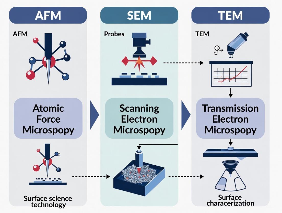
AFM vs SEM vs TEM: A Comprehensive Guide to Surface Characterization Techniques for Drug Development
This article provides a detailed comparison of Atomic Force Microscopy (AFM), Scanning Electron Microscopy (SEM), and Transmission Electron Microscopy (TEM) for surface characterization in biomedical research and drug development.
AFM vs SEM vs TEM: A Comprehensive Guide to Surface Characterization Techniques for Drug Development
Abstract
This article provides a detailed comparison of Atomic Force Microscopy (AFM), Scanning Electron Microscopy (SEM), and Transmission Electron Microscopy (TEM) for surface characterization in biomedical research and drug development. It covers the foundational principles, sample preparation and application workflows, common troubleshooting and optimization strategies, and a rigorous validation framework for technique selection. Designed for researchers and scientists, this guide synthesizes current methodologies to empower informed decision-making for analyzing nanoparticles, biomaterials, drug formulations, and cellular interfaces.
Understanding the Core Principles: How AFM, SEM, and TEM Work for Surface Analysis
This guide serves as a technical introduction to high-resolution surface characterization, a critical discipline in materials science, nanotechnology, and drug development. The ability to visualize and quantify surface topography, composition, and properties at the nanoscale directly informs the design of pharmaceuticals, medical devices, and advanced materials. This discussion is framed within a comparative thesis on three cornerstone techniques: Atomic Force Microscopy (AFM), Scanning Electron Microscopy (SEM), and Transmission Electron Microscopy (TEM). Each method offers unique capabilities and limitations, making the selection of the appropriate tool paramount for specific research questions.
Core Principles and Comparative Thesis
The choice between AFM, SEM, and TEM is dictated by the nature of the sample and the type of information required. AFM provides three-dimensional topographical data and can measure mechanical and electrical properties without requiring conductive coatings or vacuum in many modes, but has a slower scan speed and smaller field of view. SEM offers a large depth of field and rapid imaging of surface morphology with high resolution, but typically requires conductive samples and provides primarily two-dimensional data. TEM delivers atomic-scale resolution and crystallographic information by transmitting electrons through an ultra-thin specimen, making it the most powerful for internal structure but also the most complex, demanding extensive sample preparation.
Quantitative Technique Comparison
The following table summarizes the key quantitative parameters for AFM, SEM, and TEM, based on current technological capabilities.
Table 1: Comparative Analysis of AFM, SEM, and TEM
| Parameter | Atomic Force Microscopy (AFM) | Scanning Electron Microscopy (SEM) | Transmission Electron Microscopy (TEM) |
|---|---|---|---|
| Best Resolution | ~0.5 nm (vertical), ~1 nm (lateral) | ~0.5 nm (high-end FE-SEM) | ~0.05 nm (spherical aberration-corrected) |
| Typical Magnification | 5x to 100,000,000x | 10x to 1,000,000x | 50x to 10,000,000x+ |
| Sample Environment | Ambient air, liquid, vacuum | High vacuum (typically) | High/Ultra-high vacuum |
| Sample Requirement | Solid, can be insulating or conductive | Solid, often requires conductive coating | Ultra-thin solid (< 100 nm thick) |
| Primary Data | 3D topography, mechanical properties (e.g., modulus, adhesion) | 2D surface morphology, composition (EDS), crystallography (EBSD) | 2D projection of internal structure, atomic arrangement, crystallography |
| Depth of Field | High (µm range) | Very High (mm range) | Low for imaging, high for diffraction |
| Key Strength | Quantitative 3D profiling, nanomechanical mapping in native conditions | Rapid imaging of large, complex surfaces, elemental analysis | Ultimate spatial and atomic resolution, defect analysis |
| Key Limitation | Slow scan speed, tip convolution effects, small scan area | Sample charging (non-conductors), sample size limited to chamber | Extensive, destructive sample prep, thin specimen requirement |
Experimental Protocols
Protocol for AFM Nanomechanical Mapping (PeakForce QNM)
Objective: To quantitatively map the elastic modulus (Young's modulus) and adhesion of a polymer blend or biological sample in ambient conditions.
- Sample Preparation: Deposit the sample (e.g., polymer film, fixed cells) on a clean, rigid substrate (e.g., mica, silicon wafer). Ensure the sample is firmly attached and dry if imaging in air.
- Probe Selection: Mount a silicon cantilever with a sharp tip (radius < 10 nm) and a known spring constant (typically 0.4 - 200 N/m, chosen based on sample stiffness). Calibrate the deflection sensitivity and spring constant using the instrument's thermal tune procedure.
- Instrument Setup: Engage the AFM in PeakForce QNM mode. Set the peak force setpoint to a low value (e.g., 100-500 pA) to minimize sample deformation. Adjust the scan rate (0.5-1 Hz) and resolution (256x256 or 512x512 pixels).
- Data Acquisition: Initiate scanning. The system will record the force-distance curve at every pixel. Key derived channels include Height (topography), DMT Modulus (elastic modulus), Adhesion, and Deformation.
- Data Processing & Analysis: Use the proprietary software (e.g., Nanoscope Analysis) to apply a plane fit or flattening to the height channel. For modulus calculation, ensure the correct tip radius and sample Poisson's ratio are input into the Derjaguin-Muller-Toporov (DMT) model. Generate and export 2D maps and histograms of the properties.
Protocol for SEM Imaging with Energy-Dispersive X-ray Spectroscopy (EDS)
Objective: To image the surface morphology and perform elemental analysis of a composite material.
- Sample Preparation: For non-conductive samples, sputter-coat with a thin (5-10 nm) layer of gold/palladium or carbon using a sputter coater. Mount the sample on an aluminum stub using conductive carbon tape or silver paste to ensure electrical grounding.
- Instrument Setup: Load the sample into the SEM chamber and pump to high vacuum (~10^-4 Pa). Select an accelerating voltage (typically 5-20 kV) suitable for the material; lower voltages reduce penetration depth for surface-sensitive imaging.
- Imaging: Using the secondary electron (SE) detector, locate the region of interest. Adjust working distance (typically 5-10 mm), stigmation, and focus to optimize image clarity. Acquire micrographs.
- EDS Analysis: Switch to the EDS detector (e.g., Silicon Drift Detector). Position the beam on a feature of interest or define a region for mapping. Set the live time for spectrum acquisition (e.g., 60 seconds). Acquire the spectrum and generate elemental maps or point/area compositions using the instrument's software (e.g., Oxford AZtec, Bruker Esprit). Apply standardless quantification routines with appropriate matrix corrections.
Protocol for TEM Sample Preparation via Focused Ion Beam (FIB) Lift-Out
Objective: To prepare an electron-transparent lamella from a site-specific region of a bulk sample (e.g., a semiconductor device or metal alloy).
- Initial Preparation: Coat the sample with a protective layer (e.g., Pt via electron beam and ion beam deposition) over the region of interest.
- Rough Milling: Using a Ga+ ion beam at high current (e.g., 30 kV, 7 nA), mill deep trenches on both sides of the protective strip, creating a freestanding lamella (~1 µm thick) attached at the bottom and sides.
- Thinning (Fine Milling): Gradually reduce the ion beam current (to 1 nA, then 300 pA, finally 50 pA) to thin the lamella to electron transparency (< 100 nm). Tilt the stage to ensure parallel milling.
- Lift-Out: Use a micromanipulator needle to weld (via Pt deposition) to the thinned lamella, cut it free, and transport it to a TEM grid.
- Attachment: Weld the lamella to the grid posts, detach the needle, and perform a final cleaning mill at low energy (5 kV) to remove surface damage (Ga+ implantation) from the lamella faces.
Visualizing the Decision Workflow
Diagram Title: Surface Characterization Technique Decision Workflow
The Scientist's Toolkit: Essential Research Reagents & Materials
Table 2: Key Reagents and Materials for High-Resolution Characterization
| Item | Function/Brief Explanation |
|---|---|
| Conductive Adhesive Carbon Tape | Used to mount non-conductive or irregular samples to SEM stubs, providing a path to ground to prevent charging artifacts. |
| Sputter Coater (Au/Pd or C target) | Deposits a thin, uniform conductive metal (Au/Pd) or carbon layer onto insulating samples for SEM imaging, or a carbon support film for TEM grids. |
| Silicon Nitride AFM Cantilevers (e.g., DNP, MLCT) | Soft cantilevers with silicon nitride tips for imaging biological samples in liquid; they minimize sample damage. |
| High-Resolution TEM Grids (e.g., Lacey Carbon, Ultra-thin Carbon) | Copper or gold grids coated with a fragile, holey carbon film that supports ultra-thin samples or nanoparticles for TEM analysis. |
| Critical Point Dryer (CPD) | Preserves delicate, hydrated samples (e.g., hydrogels, biological tissues) for SEM/AFM by replacing water with liquid CO₂ and removing it without surface tension-induced collapse. |
| Focused Ion Beam (FIB) System | An instrument combining a high-resolution SEM with a Ga+ ion beam for precise site-specific milling, deposition, and TEM lamella preparation. |
| EDS Calibration Standard (e.g., Cobalt) | A known reference material used to calibrate the energy scale and detector performance of the Energy-Dispersive X-ray Spectrometer for accurate elemental quantification. |
This technical guide details the principle of physical probe-sample interaction in Atomic Force Microscopy, a cornerstone of nanoscale surface characterization. Within the broader thesis of comparing AFM to Scanning Electron Microscopy (SEM) and Transmission Electron Microscopy (TEM), AFM's unique value lies in its ability to provide three-dimensional topographical data and measure nanomechanical properties without the need for high vacuum or conductive coatings, making it indispensable for analyzing soft, biological, and insulating materials critical in pharmaceutical research.
Core Physical Principles
The fundamental operation of AFM relies on the detection of forces between a sharp probe and the sample surface. A microfabricated silicon or silicon nitride cantilever with a sharp tip (typical radius: 5-20 nm) is brought into close proximity with the sample. Forces—including van der Waals, electrostatic, capillary, magnetic, or chemical—cause the cantilever to deflect. This deflection is measured, typically via a laser beam reflected from the back of the cantilever onto a position-sensitive photodetector (PSPD). The resulting signal is used to generate an image or map of the surface property.
Key Force Regimes and Imaging Modes
AFM operation is categorized based on the nature of the tip-sample interaction.
| Imaging Mode | Tip-Sample Interaction | Typical Force Range | Primary Application | Advantage for Drug Research |
|---|---|---|---|---|
| Contact Mode | Repulsive (Hard contact) | 0.1 - 100 nN | High-resolution topography, friction imaging | Fast scanning, good for rigid samples. |
| Non-Contact Mode | Attractive (van der Waals) | ~10 pN | Low-stress imaging of soft materials | Minimal sample deformation. |
| Tapping Mode | Intermittent contact | 0.1 - 1 nN (peak force) | High-res imaging of soft, adhesive, or fragile samples | Prevents lateral shear forces, ideal for biomolecules, cells, polymers. |
| PeakForce Tapping | Precisely controlled, cyclic contact | 10 - 500 pN (setpoint) | Quantitative nanomechanical mapping (QNM) | Simultaneous topography and modulus/adhesion mapping of drug particles or delivery systems. |
Quantitative Force-Distance Analysis
The force-versus-distance curve is the fundamental quantitative measurement, revealing material properties.
| Parameter | Definition | Typical Values (e.g., Polymer in Buffer) | Interpretation |
|---|---|---|---|
| Adhesion Force | Maximum negative force upon retraction | 0.05 - 5 nN | Strength of tip-sample bonding (e.g., ligand-receptor). |
| Elastic Modulus | Derived from slope of repulsive region | 1 MPa - 10 GPa | Sample stiffness; key for lipid bilayers, tablets. |
| Deformation | Depth of indentation at set force | 0.5 - 10 nm | Sample compliance. |
| Energy Dissipation | Hysteresis area between approach/retract | 0.1 - 100 eV/cycle | Sample viscoelasticity. |
Detailed Experimental Protocols
Protocol 1: Imaging a Liposome Drug Delivery Vehicle in Fluid (Tapping Mode)
Objective: Obtain high-resolution topography of liposome morphology without deformation.
- Cantilever Selection: Use a sharp, silicon nitride cantilever (k ≈ 0.1 N/m, f₀ ≈ 10-30 kHz in fluid).
- Sample Preparation: Adsorb diluted liposome suspension onto freshly cleaved mica. Incubate 15 min, rinse gently with imaging buffer (e.g., PBS).
- Fluid Cell Assembly: Mount sample, install cantilever, and fill fluid cell with buffer, avoiding bubbles.
- Laser Alignment: Align laser spot on cantilever end and center reflected beam on PSPD.
- Engagement: Approach surface automatically until system detects a change in cantilever oscillation.
- Parameter Optimization:
- Set drive frequency slightly below the damped resonant frequency.
- Adjust amplitude setpoint to ~80% of free air amplitude for stable, low-force imaging.
- Optimize feedback gains to track topography accurately.
- Scanning: Acquire images at 512 x 512 pixels with a scan rate of 0.5-1.5 Hz.
Protocol 2: Measuring Young's Modulus of a Protein Aggregates (PeakForce QNM)
Objective: Quantify nanomechanical stiffness variations within protein samples.
- Probe Calibration: Pre-calibrate cantilever spring constant (k) using thermal tune method. Calibrate optical lever sensitivity on a rigid sapphire sample.
- Tip Characterization: Determine tip radius using a characterized sharp grating (e.g., TGZ1).
- Sample Preparation: Deposit protein solution on substrate, air dry or image in relevant buffer.
- Setup: Engage in PeakForce Tapping mode using a stiff probe (k ≈ 0.5 - 5 N/m).
- Parameter Setting:
- Set Peak Force setpoint to 100-500 pN (minimizing indentation).
- Set PeakForce frequency to 0.25-2 kHz.
- Select appropriate mechanical model (e.g., DMT model) in software.
- Data Acquisition: Scan while recording height, PeakForce error, and modulus channels. Capture multiple force curves per pixel.
- Analysis: Use software to fit the retraction portion of thousands of force curves with the chosen model to generate a spatial modulus map.
The Scientist's Toolkit: Key Research Reagent Solutions
| Item | Function in AFM Experiments |
|---|---|
| Silicon Nitride Probes (e.g., MLCT-Bio) | Soft cantilevers (k=0.01-0.1 N/m) for contact mode imaging of biological samples in fluid. |
| Phosphorus (n) Doped Silicon Probes (e.g., RTESPA-300) | Stiff cantilevers (k=20-80 N/m) with sharp tips for high-res Tapping Mode in air. |
| PeakForce Tapping Probes (e.g., ScanAsyst-Fluid+) | Proprietary probes with optimized geometry and reflective coating for automated, low-force imaging in buffer. |
| Ultra-Sharp Tips (e.g., SSS-NCHR) | Tips with radius < 5 nm for achieving molecular resolution. |
| Freshly Cleaved Mica Substrates | Atomically flat, negatively charged surface for adsorbing biomolecules, nanoparticles, or cells. |
| Functionalized Probes (Amino, Carboxyl, PEG) | Tips chemically modified for force spectroscopy studies of specific molecular interactions (e.g., antibody-antigen). |
| Calibration Gratings (e.g., TGZ, PPS, GRAT) | Samples with known pitch and height for verifying scanner accuracy and tip geometry. |
Comparison in Characterization Thesis Context
To position AFM's probe interaction within the thesis on surface characterization techniques, the following comparative framework is essential.
| Characteristic | AFM (Probe Interaction) | SEM | TEM |
|---|---|---|---|
| Resolution | Sub-nm vertical, ~1 nm lateral (ideal) | ~0.5 nm - 5 nm | < 0.1 nm (atomic) |
| Environment | Air, liquid, vacuum | High vacuum (typically) | High vacuum |
| Sample Prep | Minimal (often none) | Conductive coating often required | Complex (ultra-thin sectioning, staining) |
| Information | 3D topography, nanomechanical, magnetic, electrical properties | 2D surface morphology, composition (with EDS) | 2D projection/internal structure, crystallography |
| Sample Damage | Potential mechanical deformation (mitigated in tapping mode) | Potential beam damage/charging | High beam damage potential |
| Primary Advantage for Drug Dev. | Measures mechanical properties and interacts with samples in native (hydrated) states; no staining needed. | Rapid imaging of bulk sample surfaces, good for particle morphology. | Unparalleled resolution for internal structure of nanoparticles, viruses. |
Visualizing AFM Operational Principles
Diagram Title: AFM Imaging Mode Decision and Feedback Loop Workflow
Diagram Title: Key Regions in a Typical AFM Force-Distance Curve
This whitepaper details the core principles of electron-beam interaction in Scanning Electron Microscopy (SEM). This analysis is framed within a broader thesis comparing Atomic Force Microscopy (AFM), SEM, and Transmission Electron Microscopy (TEM) for surface characterization research. While AFM provides exceptional topographic and mechanical property data at atomic resolution without requiring a vacuum, and TEM offers unparalleled high-resolution internal structural information from thin samples, SEM occupies a critical niche. It excels at providing detailed, three-dimensional-like surface morphology and compositional data from bulk specimens with minimal preparation, making it indispensable for researchers and drug development professionals studying complex, non-conductive, or delicate materials.
Fundamental Principles of Electron-Sample Interaction
When a focused, high-energy primary electron beam (typically 0.1–30 keV) strikes a solid sample, it generates a variety of signals from an interaction volume beneath the surface. The nature and depth of this volume depend on the beam energy and the sample's atomic number (Z).
Key Emission Products and Their Origins
| Signal Type | Origin Depth | Primary Information Provided | Key Use in SEM |
|---|---|---|---|
| Secondary Electrons (SE) | 1-10 nm (surface) | Topography, surface electric fields | Standard imaging for 3D morphology |
| Backscattered Electrons (BSE) | 100 nm - 1 µm | Atomic number contrast (Z-contrast), crystallography | Phase distribution, grain orientation |
| Characteristic X-rays | 1-5 µm | Elemental composition | Energy-Dispersive X-ray Spectroscopy (EDS) |
| Auger Electrons | 0.5-5 nm (extreme surface) | Surface elemental composition (light elements) | Auger Electron Spectroscopy (AES) |
| Cathodoluminescence (CL) | µm range | Electronic structure, defects, impurities | Semiconductor, geology, biology |
The interaction volume is teardrop-shaped, with its size governed by the beam energy and sample density. Lower beam energies and higher atomic numbers result in a smaller interaction volume, improving surface sensitivity.
Detailed Experimental Protocol for Standard SEM Imaging
Objective: To acquire high-resolution secondary electron (SE) and backscattered electron (BSE) images of a sample.
Materials & Reagents:
- SEM Sample Stub: A conductive metal mount (typically aluminum) to hold the specimen.
- Conductive Adhesive: Carbon tape or silver paste to ensure electrical contact between sample and stub, preventing charge accumulation.
- Sputter Coater: A device used to deposit an ultra-thin (2-20 nm) conductive coating (gold, gold/palladium, platinum, or carbon) onto non-conductive samples.
- Critical Point Dryer (for biological samples): Preserves delicate structures by replacing water with liquid CO₂, then removing it under supercritical conditions to avoid surface tension damage.
Procedure:
- Sample Preparation:
- Clean the sample stub with solvent (e.g., acetone) and apply conductive adhesive.
- Mount the sample securely. For powders, disperse them on the tape.
- For non-conductive samples (e.g., polymers, biological tissue), place the mounted sample in a sputter coater. Evacuate the chamber and apply a coating under argon plasma.
- Loading into SEM:
- Secure the stub into the SEM specimen holder.
- Insert the holder into the load-lock chamber of the SEM. Evacuate the load-lock to rough vacuum.
- Transfer the holder into the main SEM chamber, achieving high vacuum (typically <10⁻³ Pa).
- Microscope Alignment & Setup:
- Turn on the high voltage (HT, typically 5-15 kV for standard imaging). Ensure the electron gun is properly saturated (for thermionic) or aligned (for field emission).
- Select a working distance (WD), often 5-10 mm. A shorter WD improves resolution but reduces depth of field.
- Select the SE or BSE detector.
- Imaging:
- Use the coarse and fine stage controls to navigate to the region of interest.
- Adjust magnification, focus, and astigmatism correction.
- Optimize contrast and brightness. For high-resolution imaging, use a slow scan speed and higher beam current.
- Acquire and save the image.
Table 1: Comparison of Key Signals for Surface Characterization
| Parameter | Secondary Electrons (SE) | Backscattered Electrons (BSE) | Characteristic X-rays (EDS) |
|---|---|---|---|
| Escape Depth | < 10 nm | 50 - 1000 nm | 1000 - 5000 nm |
| Lateral Resolution | 1 - 10 nm (depends on probe size) | 50 - 200 nm | 1000 - 2000 nm (µm scale) |
| Primary Information | Topography, morphology | Atomic number contrast, phases | Quantitative elemental composition |
| Beam Energy Typical Use | 1 - 15 keV | 10 - 30 keV | > 15 keV (to excite inner-shell electrons) |
| Key Limitation | Limited compositional data | Lower topographic contrast | Poor spatial resolution, bulk signal |
Table 2: Operational Comparison: AFM vs. SEM vs. TEM for Surface Analysis
| Feature | SEM | AFM | TEM |
|---|---|---|---|
| Resolution (Surface) | ~1 nm | < 0.5 nm (atomic) | ~0.05 nm (atomic) (for thin samples) |
| Sample Environment | High Vacuum (typically) | Air, Liquid, Vacuum | High Vacuum |
| Sample Type | Bulk (mm scale) | Bulk (mm scale) | Thin Foils (< 100 nm) |
| Primary Surface Data | 3D Topography, Composition | 3D Topography, Mechanical Properties | 2D Projection, Atomic Structure |
| Sample Preparation | Moderate (coating often needed) | Minimal | Extensive & Destructive (thinning) |
| Quantitative Data | EDS composition, Roughness | Height, Roughness, Modulus, Adhesion | Crystallography, Lattice spacing |
The Scientist's Toolkit: Essential Research Reagent Solutions
Table 3: Key Materials for SEM Sample Preparation
| Item | Function/Explanation |
|---|---|
| Carbon Conductive Tape | Double-sided adhesive tape with carbon particles. Provides both adhesion and electrical conductivity to prevent charging. |
| Silver Paint/Epoxy | Highly conductive adhesive for creating a robust electrical path from sample to stub, crucial for non-flat samples. |
| Gold/Palladium (Au/Pd) Target | Sputtering target for coating. Au/Pd provides a fine-grained, highly conductive coating for high-resolution SE imaging. |
| Carbon Evaporation Rods | High-purity carbon rods for thermal evaporation coating. Produces a thinner, less granular coating than sputtering, preferred for EDS analysis and high-resolution BSE imaging. |
| Critical Point Dryer (CPD) Supplies | Includes dehydration solvents (ethanol, acetone) and liquid CO₂. Essential for preserving the native 3D structure of hydrated biological samples (e.g., tissues, hydrogels, aerogels). |
| Conductive Liquid (e.g., OTOTO) | A staining protocol (Osmium-Thiocarbohydrazide-Osmium) that incrementally coats biological structures with osmium, enhancing conductivity and structural preservation. |
Visualizing Electron-Beam Interaction and Imaging Workflow
Diagram Title: Electron-Beam Interaction and Signal Detection in SEM
Diagram Title: Standard SEM Sample Preparation and Imaging Workflow
In a thesis comparing Atomic Force Microscopy (AFM), Scanning Electron Microscopy (SEM), and Transmission Electron Microscopy (TEM) for surface characterization research, TEM represents the pinnacle of spatial resolution. While AFM provides topographical data without requiring a vacuum and SEM offers detailed surface imaging with depth of field, TEM's unique capability lies in transmitting electrons through an ultrathin specimen to reveal internal microstructure, crystallography, and even atomic-scale details. This principle of electron transmission is fundamental to its superiority in resolution but imposes stringent sample preparation requirements compared to AFM and SEM.
Core Principle: Electron Transmission and Interaction
In TEM, a high-energy electron beam (typically 60-300 keV) is generated by a thermionic or field emission gun and accelerated through a column under high vacuum. Unlike SEM, where electrons are scanned across a surface and secondary or backscattered electrons are collected, in TEM, the primary beam is transmitted through a specimen thin enough to be partially transparent to electrons (typically <100 nm). The interaction of the beam with the specimen generates a variety of signals, but it is the transmitted portion of the beam that forms the image.
The interaction volume is minimal due to the thin sample, leading to superior resolution. The transmitted electrons carry information about the sample's internal structure. Variations in electron density, crystal orientation, and atomic number within the specimen cause localized differences in electron scattering.
Key Interaction Mechanisms:
- Elastic Scattering: Involves no energy loss; electrons are deflected by the electrostatic field of atomic nuclei. This is the primary source of contrast in crystalline materials (diffraction contrast) and high-resolution phase-contrast imaging.
- Inelastic Scattering: Involves energy loss to the specimen, causing ionization, phonon excitation, or plasmon oscillations. This provides spectroscopic information (via EELS) but contributes to chromatic aberration in imaging.
The objective lens forms a diffraction pattern in its back focal plane and a magnified image in its image plane. Subsequent intermediate and projector lenses further magnify either pattern onto the viewing screen or detector.
Quantitative Comparison of Microscopy Techniques
Table 1: Core Operational Parameters: TEM vs. SEM vs. AFM
| Parameter | Transmission Electron Microscope (TEM) | Scanning Electron Microscope (SEM) | Atomic Force Microscope (AFM) |
|---|---|---|---|
| Primary Signal | Transmitted electrons | Secondary/Backscattered electrons | Probe-Surface Force |
| Resolution | < 0.05 nm (HRTEM) | 0.5 - 3 nm | ~ 0.1 nm (vertical), ~ 1 nm (lateral) |
| Typical Operating Environment | High Vacuum (<10⁻⁵ Pa) | Vacuum (High to Low) | Ambient, Liquid, Vacuum |
| Maximum Sample Size | ~3 mm diameter, <100 nm thickness | ~200 mm diameter, ~80 mm height | ~200 mm diameter, ~20 mm height |
| Primary Imaging Mode | Transmission (Bulk internal structure) | Surface Topography & Composition | Surface Topography (3D) |
| Key Sample Constraint | Electron-transparent thin section | Must be vacuum-compatible, conductive (or coated) | Any solid surface (conductive or not) |
| Key Analytical Capabilities | SAED, EDS, EELS | EDS, EBSD, CL | Electrical, Magnetic, Mechanical Property Mapping |
Table 2: Electron-Specimen Interaction Products & Their Use in TEM
| Interaction Product | Information Provided | Primary Detector/Technique | Key Application in Research |
|---|---|---|---|
| Unscattered / Elastically Scattered Electrons | Mass-density, thickness, crystallographic phase | Bright-field (BF) Detector | General morphology, crystallographic contrast |
| Diffracted Electrons | Crystal structure, orientation, strain | Selected Area Electron Diffraction (SAED) | Phase identification, crystal defect analysis |
| Inelastically Scattered Electrons | Elemental composition, bonding states, electronic properties | Electron Energy Loss Spectrometer (EELS) | Nanoscale elemental & chemical analysis |
| Characteristic X-rays | Elemental composition (Z > 4) | Energy Dispersive X-ray Spectrometer (EDS) | Qualitative & quantitative elemental mapping |
Detailed Experimental Protocols
Protocol 1: Preparation of a Biological Sample (e.g., Protein Complex) for TEM Imaging
This protocol is critical for drug development research studying drug-target interactions.
Negative Staining (for rapid structural assessment):
- Sample Application: Apply 3-5 µL of purified protein solution (~0.1 mg/mL) to a glow-discharged carbon-coated TEM grid for 60 seconds.
- Blotting: Wick away excess liquid with filter paper.
- Staining: Immediately apply 3-5 µL of 2% (w/v) aqueous uranyl acetate stain for 45 seconds.
- Blotting & Drying: Blot away stain and air-dry the grid completely.
- Imaging: Insert grid into TEM. Use low-dose techniques (beam intensity < 10 e⁻/Ų/s) at 80-120 kV to minimize radiation damage.
Cryo-Electron Microscopy (Cryo-EM) for High-Resolution Structure:
- Vitrification: Apply 3 µL of sample to a holey carbon grid. Blot with filter paper in a climate-controlled vitrification device (e.g., Vitrobot) at >95% humidity for 2-4 seconds.
- Plunge-Freezing: Rapidly plunge the blotted grid into liquid ethane cooled by liquid nitrogen to form a vitreous ice layer.
- Transfer & Storage: Transfer grid under liquid nitrogen to a cryo-holder and maintain at <-170 °C.
- Data Collection: Image at 200-300 kV using a direct electron detector. Collect a movie series (e.g., 40 frames) at a total dose of ~40-60 e⁻/Ų to allow for motion correction.
Protocol 2: Preparation of a Material Science Sample (e.g., Nanoparticle Catalyst) via Focused Ion Beam (FIB) Lift-Out
This protocol produces an electron-transparent lamella from a specific site.
- Protective Coating: Apply a protective layer of electron-beam and ion-beam deposited platinum over the region of interest.
- Rough Milling: Use a high-current Ga⁺ ion beam (e.g., 30 keV, 9 nA) to mill trenches on both sides of the protected area, leaving a thin wall (~1 µm thick).
- Lift-Out: Attach a micromanipulator needle to the wall, cut it free, and transfer it to a TEM half-grid.
- Welding & Thinning: Weld the lamella to the grid with ion-beam deposited platinum. Systematically thin the lamella using progressively lower ion currents (from 1 nA to 50 pA) until it is electron-transparent (<100 nm).
- Final Cleaning: Perform a low-energy (2-5 keV) ion polish to remove amorphous damage layer.
Signaling Pathways and Workflow Diagrams
Diagram Title: TEM Optical Path and Information Flow
Diagram Title: Decision Logic: Choosing TEM, SEM, or AFM
The Scientist's Toolkit: Key Reagent Solutions for TEM
Table 3: Essential Research Reagents & Materials for TEM Sample Preparation
| Item | Primary Function & Explanation |
|---|---|
| Holey Carbon Grids (Quantifoil, C-flat) | TEM support film with regular holes. Allows sample suspension over vacuum for cryo-EM, preventing background noise from a continuous film. |
| Uranyl Acetate (2% aqueous) | Negative Stain. Heavy metal salt that surrounds, but does not penetrate, biological macromolecules. Enhances contrast by scattering electrons away from the stained areas. |
| Glutaraldehyde (2-4% in buffer) | Chemical Fixative. Cross-links proteins and stabilizes cellular structures by forming covalent bonds between amine groups, preserving morphology during dehydration. |
| Osmium Tetroxide (1-2% aqueous) | Post-fixative & Stain. Reacts with lipids and unsaturated bonds, both stabilizing membranes and adding electron density (stain) to lipid-rich structures. |
| Ethanol & Acetone (Graded Series) | Dehydration Agents. Gradually replace water in biological samples to prepare for resin infiltration. Critical to prevent specimen collapse. |
| Epoxy Resin (Epon, Spurr's) | Embedding Medium. Infiltrates dehydrated tissue and polymerizes into a hard block, allowing ultrathin sectioning (50-100 nm) with a diamond knife. |
| Liquid Ethane | Cryogen for Vitrification. Its high thermal conductivity enables rapid cooling of aqueous samples (>10⁴ K/s), forming non-crystalline (vitreous) ice, preserving native hydrated state. |
| Triple-Axis Ion Polisher (e.g., Fischione) | Final Sample Thinning. Uses low-energy Ar⁺ ions to gently remove amorphous surface damage from FIB-prepared lamellae, achieving a pristine, electron-transparent surface. |
Within the landscape of surface characterization techniques, selecting the appropriate instrument is critical for research and development, particularly in fields like drug development where nanoscale detail is paramount. This guide provides a technical comparison of three cornerstone microscopy techniques—Atomic Force Microscopy (AFM), Scanning Electron Microscopy (SEM), and Transmission Electron Microscopy (TEM)—focusing on their defining operational parameters. The core thesis is that while AFM, SEM, and TEM can all probe the nanoscale, their fundamental principles lead to distinct, often complementary, profiles in resolution, depth of field, and field of view, making instrument choice inherently application-dependent.
Fundamental Principles & Parameter Definitions
- AFM: A scanning probe technique that uses a physical tip to raster-scan a surface, measuring interatomic forces to generate a topographical map. It provides true 3D data.
- SEM: Uses a focused beam of high-energy electrons scanned across a surface. Detectors capture signals from electron-sample interactions (e.g., secondary electrons) to create a 2D intensity image.
- TEM: Transmits a beam of high-energy electrons through an ultra-thin specimen. The image is formed from variations in electron transmission and scattering, revealing internal structure at atomic scales.
Key Parameter Definitions:
- Lateral Resolution: The minimum distance between two distinguishable points in the plane of the sample (x-y).
- Vertical Resolution: The minimum detectable height difference (z). Critical for roughness measurements.
- Atomic Resolution: The ability to resolve individual atoms or atomic lattices.
- Depth of Field (DoF): The vertical distance (along the z-axis) within which the sample remains in acceptable focus.
- Field of View (FoV): The maximum area of the sample that can be imaged in a single scan or frame.
Comparative Analysis of Key Parameters
The following table synthesizes current data on the core parameters for the three techniques.
Table 1: Comparative Performance Parameters of AFM, SEM, and TEM
| Parameter | Atomic Force Microscopy (AFM) | Scanning Electron Microscopy (SEM) | Transmission Electron Microscopy (TEM) |
|---|---|---|---|
| Lateral Resolution | ~0.5 nm (Ambient) <0.1 nm (Ultra-High Vacuum) | 0.5 nm – 5 nm (High-vacuum, Field Emission Gun) | 0.05 nm – 0.2 nm (Spherical Aberration Corrected) |
| Vertical Resolution | <0.1 nm (exceptional) | Not inherently 3D; stereoscopy required for height data. | Not applicable (2D projection). |
| Atomic Resolution | Yes, on conductive & insulating surfaces. Resolves atomic lattices. | No. Resolves nanoscale features but not individual atoms on surfaces. | Yes. Resolves individual atoms and crystal lattices in projection. |
| Depth of Field | Very low (due to tip-sample proximity). Microns at most. | Very High (mm range for large working distances). | High (for thin specimens), but specimen thickness limits. |
| Field of View | Typically <150 µm x 150 µm. Maximum ~100 µm. | Large. Easily from mm to sub-µm by changing magnification. | Small. Limited to the specimen grid hole (µm scale). |
| Sample Environment | Ambient, liquid, vacuum. | High vacuum typical; ESEM allows hydrated samples. | High/Ultra-high vacuum only. |
| Sample Preparation | Minimal. | Often requires conductive coating for non-conductors. | Extensive: thinning to <100 nm, often via FIB or ion milling. |
| Information Type | True 3D topography, mechanical/electrical properties. | 2D surface morphology, composition (with EDS). | 2D projection of internal structure, crystallography, composition. |
Experimental Protocols for Cited Techniques
Protocol 1: AFM for High-Resolution Topography in Fluid
- Objective: Acquire sub-nanometer vertical resolution topography of a lipid bilayer or protein sample in physiological buffer.
- Materials: AFM with fluid cell, sharp nitride lever probe (k ~0.1 N/m), sample substrate (e.g., mica), appropriate buffer.
- Sample Preparation: Cleave a fresh mica surface. Deposit the biomolecular sample (e.g., via vesicle fusion) and incubate in buffer.
- Probe & System Setup: Install the probe in the fluid cell. Fill the cell with degassed buffer, ensuring no air bubbles are trapped.
- Engagement: Use the optical microscope to position the probe above the sample. Initiate automatic engagement in fluid.
- Tuning: Tune the cantilever resonance frequency in fluid. Set a low amplitude and a low integral gain to minimize imaging force (<100 pN).
- Imaging: Select a scan area (e.g., 1 µm x 1 µm). Use a slow scan rate (0.5-2 Hz) to allow the tip to track the surface accurately. Acquire images in tapping or contact mode.
- Analysis: Apply first-order flattening to remove sample tilt. Analyze height profiles and surface roughness using instrument software.
Protocol 2: SEM Imaging of a Non-Conductive Pharmaceutical Powder
- Objective: Obtain a high-depth-of-field image of particle morphology without charging artifacts.
- Materials: High-vacuum or field-emission SEM, sputter coater, gold/palladium target, conductive adhesive tape, sample stub.
- Sample Mounting: Apply conductive carbon tape to an aluminum stub. Lightly sprinkle the powder onto the tape. Use compressed air to remove loose, non-adhered particles.
- Conductive Coating: Load the stub into a sputter coater. Evacuate the chamber and perform a ~10-20 nm coating with gold/palladium under an argon atmosphere.
- SEM Loading & Pump Down: Transfer the coated stub to the SEM sample chamber. Evacuate to high vacuum (typically <10^-5 mbar).
- Alignment & Parameters: At low magnification (e.g., 500x), align the electron column. Move to the region of interest. For high resolution, use a low accelerating voltage (1-5 kV) and a short working distance (2-5 mm) to reduce charging and increase resolution.
- Image Acquisition: Adjust contrast and brightness using the detector signal. Capture images at varying magnifications to show both overall distribution and fine surface details.
Protocol 3: TEM for Atomic-Scale Lattice Imaging
- Objective: Resolve the atomic lattice planes of a crystalline nanoparticle catalyst.
- Materials: Aberration-corrected TEM, holey carbon TEM grid, ultrasonic disperser, appropriate solvent.
- Specimen Preparation: Disperse nanoparticles in ethanol via ultrasonication for 5-10 minutes. Pipette a drop of the suspension onto a TEM grid and allow it to dry.
- TEM Alignment: Load the grid into a double-tilt holder and insert into the TEM. Align the microscope: gun tilt, condenser stigmator, voltage center.
- Specimen Positioning: At low magnification, locate a suitable thin area where nanoparticles overlap a hole in the carbon support.
- High-Resolution Mode: Switch to high magnification (>600k x). Perform fine beam alignment and stigmation. Activate the aberration corrector and optimize tuning.
- Imaging: Use a small objective aperture if needed. Defocus slightly (Scherzer defocus) to optimize phase contrast. Acquire a series of images with short exposure times to minimize drift and radiation damage.
- Calibration: Record a diffraction pattern from the same area or a known standard (e.g., gold) to calibrate the image scale for lattice spacing measurement.
Visualization of Technique Selection Logic
Title: Logic Flow for Selecting AFM, SEM, or TEM
The Scientist's Toolkit: Essential Research Reagents & Materials
Table 2: Key Reagents and Materials for Featured Microscopy Techniques
| Item | Primary Function | Typical Application Context |
|---|---|---|
| Freshly Cleaved Mica | Atomically flat, negatively charged substrate. | Ideal substrate for AFM imaging of biomolecules (proteins, DNA, lipid bilayers) in air or liquid. |
| Holey Carbon TEM Grid | Supports ultra-thin specimens while providing regions with no background for imaging. | Standard support film for TEM analysis of nanoparticles, macromolecules, and thin materials. |
| Gold/Palladium (Au/Pd) Target | Source material for sputter coating. | Creates a thin, conductive metal layer on non-conductive samples (e.g., polymers, biological tissue) for SEM to prevent charging. |
| Conductive Carbon Tape | Provides both adhesion and electrical conduction from sample to stub. | Used universally in SEM for mounting powders, flakes, and solid samples to aluminum stints. |
| Silicon Nitride AFM Probes | Microfabricated cantilevers with sharp tips (spring constants from 0.01 to 1 N/m). | The sensing element for AFM. Softer levers are used for biological samples in fluid; stiffer levers for ambient tapping mode. |
| Ion Milling System (e.g., FIB) | Uses focused ion beams (Ga+) to precisely cut and thin materials. | Critical for preparing site-specific, electron-transparent lamellae from bulk materials for TEM analysis. |
| Critical Point Dryer | Removes solvent from hydrated samples without surface tension-induced collapse. | Essential preparation step for imaging delicate biological structures (e.g., cells, hydrogels) in high-vacuum SEM. |
| Crystallographic Standard (e.g., Gold Nanoparticles) | Provides known diffraction patterns and lattice spacings. | Used to calibrate magnification and camera length in TEM for accurate measurement of unknown samples. |
Within the framework of selecting the optimal surface characterization technique—Atomic Force Microscopy (AFM), Scanning Electron Microscopy (SEM), and Transmission Electron Microscopy (TEM)—the sample environment is a critical, often decisive, factor. This guide provides an in-depth technical comparison of vacuum, ambient, and liquid condition requirements, detailing their implications for research, particularly in life sciences and drug development.
Core Environmental Requirements & Technical Specifications
The operational environment fundamentally dictates which technique can be employed and what sample information can be retrieved.
Table 1: Comparative Environmental Specifications for AFM, SEM, and TEM
| Parameter | Atomic Force Microscopy (AFM) | Scanning Electron Microscopy (SEM) | Transmission Electron Microscopy (TEM) |
|---|---|---|---|
| Primary Environment | Ultra-high vacuum to liquid (full range). | High vacuum (typical), variable pressure/low vacuum (VP-SEM), environmental (ESEM). | Ultra-high vacuum (UHV), typically ≤ 10⁻⁴ Pa. |
| Ambient Air Compatibility | Yes. Standard operation. | No (standard SEM). Yes (VP/ESEM with specialized detector). | No. |
| Liquid Cell Compatibility | Yes. Native state imaging in buffer solutions. | Limited. Specialized ESEM or closed cells for hydration; not for bulk liquid. | Yes. Specialized in situ liquid holders with thin electron-transparent windows. |
| Typical Pressure Range | 10⁵ Pa (ambient) to 10⁻⁸ Pa (UHV in certain modes). | 10⁻³ to 10⁻⁶ Pa (High Vac), up to 2500 Pa (ESEM). | ≤ 10⁻⁴ Pa, often 10⁻⁷ Pa. |
| Sample Hydration State | Can be fully hydrated, partially hydrated, or dry. | Dry (High Vac), hydrated (ESEM). | Typically dry; hydrated only in specialized liquid cells. |
| Key Environmental Limitation | Minimal. Cantilever damping in viscous liquids. | Electron scatter in gaseous environments reduces resolution. | Mean free path of electrons; liquid layer thickness drastically limits resolution. |
Detailed Methodologies for Key Experiments
Protocol 1: Imaging Protein Complexes in Liquid Using AFM
Objective: To visualize the structure and dynamics of membrane proteins in a physiological buffer.
- Substrate Preparation: Cleave a sheet of Muscovite mica (V1 grade) using adhesive tape to create an atomically flat surface. Functionalize with 0.01% poly-L-lysine for 5 minutes, then rinse with ultrapure water.
- Sample Preparation: Dilute the purified protein complex (e.g., a GPCR) in a suitable imaging buffer (e.g., 20 mM HEPES, 150 mM KCl, pH 7.4) to a concentration of ~5-10 µg/mL.
- Adsorption: Pipette 50 µL of the sample solution onto the mica substrate. Incubate for 10-15 minutes in a humidity chamber.
- Liquid Cell Assembly: Rinse the substrate gently with 2 mL of imaging buffer to remove unbound protein. Mount the mica disc into the AFM liquid cell and fill the cell with ~100 µL of imaging buffer, ensuring no air bubbles are present.
- Imaging: Mount the cell on the AFM scanner. Engage a silicon nitride cantilever (k ~0.1 N/m, f₀ ~10 kHz in liquid) using the fluid engage procedure. Perform imaging in AC (Tapping) mode in liquid to minimize lateral forces. Set a low scan rate (1-2 Hz) for optimal signal-to-noise.
Protocol 2: Imaging Hydrated Polymer Micelles Using Environmental SEM (ESEM)
Objective: To characterize the morphology of drug-loaded polymeric micelles without desiccating the sample.
- Sample Preparation: Deposit 10 µL of the aqueous micelle suspension onto a clean, polished aluminum specimen stub. Do not coat with conductive material.
- ESEM Chamber Preparation: Cool the Peltier stage to 2°C. Introduce water vapor as the imaging gas. Adjust the chamber pressure to 700 Pa (5.2 Torr) to maintain a 100% relative humidity environment at the stage temperature.
- Loading and Equilibration: Transfer the stub to the pre-cooled stage. Allow 5-10 minutes for temperature and pressure stabilization to prevent condensation or evaporation.
- Imaging Parameters: Use a gaseous secondary electron detector (GSED). Accelerating voltage: 15-20 kV. Working distance: 5-10 mm. Slowly decrease the chamber pressure in small increments (e.g., 50 Pa steps) to achieve controlled slight dehydration, which stabilizes the sample and improves contrast. Image immediately upon achieving a stable, semi-hydrated state.
Protocol 3: High-Resolution Imaging of Nanoparticles in High Vacuum SEM
Objective: To achieve maximum resolution for metal nanoparticle size and distribution analysis.
- Substrate Preparation: Use a conductive substrate, such as a silicon wafer with a native oxide layer or a TEM grid on a SEM stub.
- Sample Preparation: Sonicate nanoparticle dispersion for 10 minutes. Drop-cast 5 µL onto the substrate and allow to dry in a clean desiccator.
- Conductive Coating: Sputter-coat the sample with a 5 nm layer of iridium (or platinum/palladium) using a high-resolution sputter coater. This minimizes charging and provides a high-secondary electron yield surface.
- High Vacuum Chamber Pump-down: Load the sample and initiate a high-vacuum pump-down sequence (rotary pump followed by turbomolecular pump) until a pressure of ≤ 5 x 10⁻⁴ Pa is achieved.
- High-Resolution Imaging: Use an in-lens or through-the-lens (TLD) detector for topographical and material contrast. Accelerating voltage: 5-10 kV (optimized to reduce interaction volume). Probe current: 10-50 pA (small spot size). Slow scan speed with frame averaging.
Visualization of Technique Selection Logic
Title: Surface Technique Selection Based on Sample Environment
The Scientist's Toolkit: Essential Research Reagent Solutions
Table 2: Key Materials for Sample Preparation Across Environments
| Item | Function & Description | Typical Application |
|---|---|---|
| Muscovite Mica (V1 Grade) | An atomically flat, negatively charged, cleavable substrate for adsorbing biomolecules and nanomaterials. | AFM in liquid/air; substrate for TEM grid preparation. |
| Poly-L-Lysine Solution | A positively charged polymer coating that promotes adhesion of cells, proteins, and negatively charged particles to substrates. | AFM sample immobilization; SEM/TEM pre-coating for biologicals. |
| Iridium Sputter Target | Source for ultra-thin, fine-grained conductive coating. Superior to gold for high-resolution imaging. | Conductive coating for high-resolution SEM and some TEM samples. |
| Glutaraldehyde (2.5% in buffer) | A cross-linking fixative that preserves protein structure and cellular architecture by forming covalent bonds. | Fixing biological samples for SEM/TEM (vacuum preparation). |
| Critical Point Dryer | Equipment that uses liquid CO₂ to remove water without surface tension-induced collapse of delicate structures. | Preparing hydrated soft materials (gels, biologicals) for high-vacuum SEM/TEM. |
| In Situ Liquid Cell (TEM/SEM) | A sealed holder with electron-transparent windows (e.g., SiN) that encapsulates a liquid environment for the sample. | Real-time TEM/SEM imaging of processes in liquid (nanoparticle growth, electrochemical reactions). |
| PELCO Conductive Carbon Tape | A double-sided, graphite-based adhesive tape for mounting samples to stubs. Minimizes charging. | Sample mounting for all vacuum-based microscopy (SEM, TEM stub mounting). |
| HEPES Buffer (1M stock) | A biological buffer effective at pH 7.2-7.4, non-reactive, and ideal for maintaining physiological conditions. | AFM liquid imaging buffer; sample preparation buffer for biological TEM/SEM. |
| Proplette Precision Pipettes | Positive displacement pipettes for handling viscous liquids (e.g., buffers with glycerol) and volatile solvents. | Precise dispensing of reagents for sample preparation across all techniques. |
Within advanced surface characterization research, selecting the appropriate technique is critical for extracting specific material properties. Atomic Force Microscopy (AFM), Scanning Electron Microscopy (SEM), and Transmission Electron Microscopy (TEM) form a cornerstone suite of tools, each offering unique and complementary insights into topography, morphology, composition, and mechanical properties. This whitepaper provides a technical guide to the core information outputs of these techniques, framed within a comparative thesis to inform methodological choices in fields such as drug development and materials science.
Core Technique Comparison: Capabilities and Limitations
The following table summarizes the principal information outputs, resolution limits, and operational constraints of AFM, SEM, and TEM.
Table 1: Comparative Analysis of AFM, SEM, and TEM for Surface Characterization
| Parameter | Atomic Force Microscopy (AFM) | Scanning Electron Microscopy (SEM) | Transmission Electron Microscopy (TEM) |
|---|---|---|---|
| Primary Topography | 3D surface profile with sub-nanometer vertical resolution. | 3D-like 2D image with nanometer lateral resolution. | Not a direct topography tool; internal structure and morphology. |
| Morphology | Excellent for surface features; resolution ~0.5 nm (lateral). | Excellent for surface and near-surface; resolution ~0.5-10 nm. | Exceptional for internal/bulk morphology; resolution <0.5 nm. |
| Composition | Limited; requires specialized modes (e.g., KPFM, chemical force). | Good; Energy-Dispersive X-Ray Spectroscopy (EDS) provides elemental analysis. | Excellent; EDS and Electron Energy-Loss Spectroscopy (EELS) for elemental/chemical state. |
| Mechanical Properties | Direct quantitative measurement (e.g., Young's modulus, adhesion, stiffness) via force spectroscopy. | Indirect, qualitative (e.g., phase contrast in BSE). | Indirect via diffraction contrast; in-situ mechanical testing possible. |
| Sample Environment | Ambient, liquid, vacuum. Non-destructive. | High vacuum typically required. Conductive coating often needed. | High vacuum required. Sample must be electron-transparent (<100 nm thick). |
| Key Limitation | Scan size limited (~150 µm); slow scan speed. | Sample must be vacuum-compatible and often conductive. | Extensive sample preparation; ultra-thin samples; potential beam damage. |
Detailed Methodologies and Protocols
Atomic Force Microscopy (AFM) for Topography and Mechanics
Protocol: Quantitative Nanomechanical Mapping (QNM) via PeakForce Tapping
- Objective: To simultaneously acquire high-resolution topography and quantitative mechanical properties maps.
- Sample Preparation: Substrate-bound samples (e.g., polymer blends, biological cells on glass) are rinsed with appropriate buffer (e.g., PBS) and gently dried or measured in fluid.
- Cantilever Calibration: Thermal tune method is used to determine the spring constant (k) of the cantilever. The optical lever sensitivity (InvOLS) is calibrated on a clean, rigid substrate (e.g., sapphire).
- Tip Selection: Use a probe with a known, sharp tip geometry (e.g., silicon tip with radius <10 nm) and a defined spring constant (typically 0.1-1 N/m for soft materials).
- Imaging Parameters: Set PeakForce frequency to 0.5-2 kHz, amplitude ~50-150 nm. Adjust the PeakForce setpoint to maintain gentle, non-destructive tip-sample interaction.
- Data Acquisition: The system records the force-distance curve at each pixel. Topography is derived from the feedback signal to maintain constant peak force. Elastic modulus (DMT model), adhesion, dissipation, and deformation are extracted from the curve analysis in real-time.
- Analysis: Use proprietary software (e.g., Nanoscope Analysis) to generate maps of modulus, adhesion, and topography. Apply appropriate contact mechanics models (DMT, Hertz) for quantitative values.
Scanning Electron Microscopy (SEM) for Morphology and Composition
Protocol: High-Resolution Imaging with Energy-Dispersive X-Ray Spectroscopy (EDS)
- Objective: To obtain high-magnification surface morphology and perform localized elemental analysis.
- Sample Preparation: For non-conductive samples (e.g., pharmaceuticals, polymers), apply a thin (~5-10 nm) conductive coating of gold/palladium or carbon via sputter coater. Mount sample on an aluminum stub using conductive carbon tape.
- Microscope Setup: Insert sample into high-vacuum chamber. For high-resolution, use a field-emission gun (FEG) source. Accelerating voltage is optimized (typically 5-15 kV) to balance surface detail and penetration depth.
- Imaging: Select appropriate detector (e.g., In-lens SE detector for surface topography, BSD for compositional contrast). Adjust working distance (e.g., 4-8 mm) and aperture size for optimal resolution.
- EDS Acquisition: Select area or point of interest. Set the live time for spectrum acquisition (e.g., 60-120 seconds) to ensure sufficient counts. Ensure the sample is tilted approximately 15° towards the EDS detector.
- Analysis: Use EDS software to identify characteristic X-ray peaks, generate elemental maps, and perform semi-quantitative weight/atomic percentage analysis using standardless or standard-based ZAF correction.
Transmission Electron Microscopy (TEM) for Nanoscale Morphology and Composition
Protocol: High-Resolution TEM (HRTEM) and Scanning TEM (STEM)-EDS Analysis
- Objective: To resolve atomic-scale lattice fringes and perform nanoscale compositional mapping.
- Sample Preparation (Ultramicrotomy): Embed sample (e.g., nanoparticle suspension) in epoxy resin. Cure and trim to a small pyramid. Section using a diamond knife to produce 50-100 nm thick slices. Collect slices on TEM grids (e.g., copper, 300 mesh).
- Microscope Alignment: Perform standard TEM alignments: gun tilt, condenser lens astigmatism, and voltage centering. For HRTEM, align the objective lens stigmator and set the correct defocus (Scherzer defocus).
- HRTEM Imaging: Insert sample, locate a thin area. Switch to high magnification (>400kX). Adjust objective lens current to achieve proper defocus. Record images using a slow-scan CCD or direct electron detection camera.
- STEM-EDS Acquisition: Switch to STEM mode with a convergent electron probe (spot size ~0.5-1 nm). Raster the probe over the region of interest. Simultaneously acquire high-angle annular dark-field (HAADF) images and collect X-ray spectra at each pixel using an EDS detector.
- Analysis: Process HRTEM images via Fast Fourier Transform (FFT) to analyze crystal planes. For STEM-EDS, reconstruct elemental maps by integrating counts under specific X-ray peaks for each element.
Visualization: Characterization Workflow and Decision Logic
Title: Characterization Technique Selection Logic
Title: Core Technique Workflow from Sample to Data
The Scientist's Toolkit: Essential Research Reagent Solutions
Table 2: Key Materials and Reagents for Advanced Surface Characterization
| Item | Function/Application | Common Example/Supplier |
|---|---|---|
| Conductive Adhesive Tabs | Mounts non-powder samples to SEM stubs; provides electrical conductivity path to prevent charging. | Carbon double-sided tape; PELCO conductive tabs. |
| Sputter Coater Targets | Source material for depositing ultra-thin conductive films (Au/Pd, Pt, C) on non-conductive samples for SEM/TEM. | Gold-Palladium (80/20) target, 2" diameter. |
| TEM Grids | Supports ultrathin samples (sections, nanoparticles) in the TEM beam. Copper is common; gold or nickel for EDS. | Copper, 300 mesh, Formvar/carbon-coated grids. |
| Ultramicrotomy Knives | Precisely sections embedded samples into slices thin enough (50-100 nm) for electron transparency in TEM. | DiATOME diamond knives (45° cutting angle). |
| Epoxy Embedding Kits | Infiltrates and rigidly supports soft or porous samples (e.g., tissues, polymers) for ultramicrotomy. | Epoxy resins (Epon 812, Spurr's). |
| AFM Probes/Cantilevers | Nanoscale tips on calibrated levers that interact with the sample surface. Selection is critical for mode/resolution. | Bruker RTESPA-300 (tapping mode); ScanAsyst-Fluid+ (PeakForce). |
| Calibration Standards | Reference samples with known dimensions or properties to verify instrument magnification and measurement accuracy. | TGQ1 (AFM pitch), NIST-traceable magnification grids (SEM/TEM). |
Practical Applications in Drug Development: Sample Prep and Imaging Protocols for AFM, SEM, and TEM
This guide provides a structured framework for selecting the most appropriate high-resolution microscopy technique—Atomic Force Microscopy (AFM), Scanning Electron Microscopy (SEM), or Transmission Electron Microscopy (TEM)—for surface characterization of biomaterials. The choice critically impacts the accuracy, relevance, and efficiency of research in drug delivery systems, implantable devices, and diagnostic platforms.
Core Technique Comparison: AFM vs. SEM vs. TEM
The following table summarizes the fundamental quantitative and qualitative parameters of each technique, crucial for initial screening.
Table 1: Core Technical Specifications and Capabilities
| Parameter | Atomic Force Microscopy (AFM) | Scanning Electron Microscopy (SEM) | Transmission Electron Microscopy (TEM) |
|---|---|---|---|
| Primary Interaction | Mechanical force (tip-sample) | Electron-sample scattering | Electron transmission |
| Lateral Resolution | ~0.5 nm (in air/liquid) | 0.5 nm - 5 nm | < 0.05 nm (sub-Ångström) |
| Vertical Resolution | ~0.1 nm | Limited (2D imaging) | Atomic column resolution |
| Max Imaging Depth | Topographic surface (≤ nm) | ~1 µm (for secondary electrons) | Sample thickness < 100-200 nm |
| Environment | Ambient, liquid, vacuum | High vacuum (typically) | High vacuum |
| Sample Conductivity | Not required | Required (often via coating) | Required (often via staining) |
| Quantitative Data | Topography, roughness, modulus, adhesion | Topography, composition (EDS), morphology | Crystallography, lattice structure, morphology |
| Key Biomaterial Application | Live cell mechanics, polymer degradation in situ, protein aggregation | Surface porosity of scaffolds, composite material morphology, coating uniformity | Internal structure of nanoparticles, lipid bilayer detail, crystal defects in bioceramics |
The Selection Framework: A Decision Workflow
The framework is based on a primary question tree that prioritizes the research question over technical capability.
Title: Decision Workflow for Technique Selection
Detailed Experimental Protocols for Biomaterials
Protocol 1: AFM Nanomechanical Mapping of a Hydrogel Film
Aim: To quantify the Young's modulus of a drug-loaded hydrogel coating in phosphate-buffered saline (PBS).
- Sample Preparation: Spin-coat hydrogel solution onto a clean glass slide. Incubate in PBS (pH 7.4) for 24h to equilibrate.
- AFM Setup: Mount liquid cell. Use a silicon nitride cantilever with a colloidal probe (sphere radius ~5 µm). Calibrate spring constant via thermal tune.
- Force Volume Imaging: Acquire a grid (e.g., 32x32 points) of force-distance curves over a 10 µm x 10 µm area. Set trigger force to 1 nN to prevent sample damage.
- Data Analysis: Fit the retract curve of each force curve with the Hertzian contact model (for elastic samples) using the AFM software. Generate a 2D modulus map and calculate average modulus ± standard deviation.
Protocol 2: SEM Imaging of a Porous Polymer Scaffold
Aim: To characterize surface pore size, distribution, and morphology of a polylactic acid (PLA) scaffold.
- Sample Preparation: Sputter-coat sample with a 10 nm layer of gold/palladium using a low-vacuum sputter coater to ensure conductivity.
- SEM Setup: Load sample into high-vacuum chamber. Set accelerating voltage to 5 kV (low voltage reduces charging and beam damage).
- Imaging: Use the secondary electron (SE) detector. Start at low magnification (500X) to locate region of interest, then increase to desired magnification (e.g., 10,000X). Adjust working distance to ~6 mm for optimal focus.
- Analysis: Use image analysis software (e.g., ImageJ) to threshold the image and measure pore diameter and circularity from at least 100 pores across multiple images.
Protocol 3: TEM Imaging of Polymeric Nanoparticles
Aim: To visualize the core-shell structure of drug-loaded PLGA-PEG nanoparticles.
- Sample Preparation: Drop-cast 5 µL of nanoparticle suspension (in water) onto a carbon-coated copper grid. Negative stain with 2% uranyl acetate for 30 seconds, then wick away excess. Air-dry completely.
- TEM Setup: Insert grid into holder. Align microscope at 80 kV (reduces damage to polymer).
- Imaging: Use a high-contrast objective aperture. Locate a suitable area at low mag. Capture images at magnifications from 25,000X to 100,000X using a CCD camera.
- Analysis: Measure core and shell dimensions. Use Fast Fourier Transform (FFT) to assess crystallinity of the core, if present.
The Scientist's Toolkit: Essential Research Reagents & Materials
Table 2: Key Reagents and Materials for Biomaterial Microscopy
| Item | Primary Function | Example Use Case |
|---|---|---|
| Conductive Tape (Carbon) | Provides electrical conductivity and adhesion for SEM mounting. | Mounting non-conductive powder samples (e.g., ceramic granules) on an SEM stub. |
| Sputter Coater (Au/Pd Target) | Deposits a thin, conductive metal layer on insulating samples. | Preparing polymeric scaffolds or biological tissues for high-resolution SEM without charging artifacts. |
| Uranyl Acetate (2% Solution) | Heavy metal negative stain that scatters electrons, enhancing contrast for TEM. | Visualizing the outline and internal structure of liposomes or protein complexes. |
| Phosphate Buffered Saline (PBS), pH 7.4 | Isotonic, biocompatible buffer for maintaining physiological conditions. | Hydrating and imaging hydrogel or biological samples in AFM liquid cell experiments. |
| Silicon Nitride AFM Probes | Cantilevers with low spring constants for soft samples, compatible with liquids. | Nanomechanical mapping of live cells or soft hydrogels in fluid. |
| Carbon-Coated TEM Grids | Provide an ultrathin, stable, and conductive support film for TEM samples. | Holding nanoparticle suspensions or ultra-microtomed sections of a polymer blend. |
| Critical Point Dryer | Removes liquid from samples without inducing surface tension collapse. | Preparing delicate, hydrated structures (e.g., collagen networks) for SEM while preserving native morphology. |
Integrated Workflow for Multi-Technique Characterization
A comprehensive study often requires correlative data from multiple techniques. The following diagram outlines a sequential workflow for characterizing a novel drug-eluting implant coating.
Title: Correlative Multi-Technique Analysis Workflow
No single microscopy technique provides a complete picture of complex biomaterial surfaces. This framework advocates for a question-driven, then capability-informed selection process. AFM is indispensable for in situ functional properties, SEM for high-throughput topographic and compositional analysis, and TEM for ultimate resolution of internal nanostructure. Strategic application, and increasingly, correlative use of these tools, is paramount for advancing biomaterials research and development.
Within the critical framework of surface characterization research, researchers choose between Atomic Force Microscopy (AFM), Scanning Electron Microscopy (SEM), and Transmission Electron Microscopy (TEM) based on specific information needs. This guide focuses on the unique niche of AFM, which is unparalleled for investigating soft, hydrated, and mechanically sensitive samples under near-physiological conditions—a domain where high-vacuum, high-energy electron beams (SEM/TEM) intrinsically fail. AFM provides not only topographical imaging but also quantitative, nanoscale maps of mechanical properties, offering a functional complement to the high-resolution structural snapshots provided by electron microscopy.
Core Imaging Modes for Delicate Samples
1. Contact Mode: The tip maintains constant contact with the sample. While straightforward, it can exert high lateral forces, making it less ideal for very soft samples like live cells. 2. Intermittent Contact (Tapping) Mode: The tip oscillates and taps the surface, minimizing lateral forces. This is the preferred mode for high-resolution imaging of soft samples and cells in fluid. 3. Non-Contact Mode: The tip oscillates above the sample surface, detecting van der Waals forces. Used for extremely soft materials where even minimal contact is undesirable.
Quantitative Nanomechanical Property Mapping
AFM-based force spectroscopy is the cornerstone of nanomechanical analysis. By recording the force-distance curve during the approach and retraction of the tip, multiple properties can be derived.
Key Properties Measured:
- Elastic Modulus (Stiffness): Derived from the slope of the indentation region in the approach curve, often using models (e.g., Hertz, Sneddon).
- Adhesion Force: Calculated from the minimum force of the retraction curve, representing the "pull-off" force required to separate the tip from the sample.
- Deformation: The sample's indentation depth at a given applied load.
- Energy Dissipation: Related to the hysteresis between approach and retraction curves, indicative of sample viscosity.
Primary Techniques:
- Force Volume Imaging: Captures a full force-distance curve at each pixel, creating spatial maps of modulus, adhesion, etc., albeit slowly.
- PeakForce QNM (Quantitative Nanomechanical Mapping): A faster, tapping-based derivative that captures a force curve at the tapping frequency, enabling high-resolution, real-time mapping of mechanical properties.
Table 1: Comparison of Key AFM Nanomechanical Measurement Techniques
| Technique | Principle | Speed | Spatial Resolution | Key Outputs | Best For |
|---|---|---|---|---|---|
| Force Volume | Force-distance curve at grid points | Slow (minutes-hours) | Medium-High (~50 nm) | Elastic Modulus, Adhesion, Deformation maps | Detailed, point-by-point analysis of heterogeneous samples |
| PeakForce QNM | Sub-nanosecond force taps at resonance | Fast (minutes) | High (<10 nm) | Real-time maps of Modulus, Adhesion, Dissipation, Deformation | High-resolution, live imaging of dynamic processes |
| Force Spectroscopy | Single point/location force curves | Fast (seconds per curve) | Single Point | Single values of Adhesion, Stiffness at chosen locations | Targeted measurements (e.g., on a specific cell organelle) |
Experimental Protocols
Protocol 1: Imaging Live Mammalian Cells in Buffer
Objective: To obtain high-resolution topographical images of live adherent cells with minimal perturbation.
- Substrate Preparation: Use a sterile 35 mm Petri dish or glass-bottom dish. Coat with Poly-L-Lysine (0.01%) or appropriate extracellular matrix protein (e.g., collagen, fibronectin) for 30 min to promote cell adhesion.
- Cell Seeding: Seed cells at a sub-confluent density (e.g., 50-70k cells/dish) in complete culture medium 24-48 hours prior to imaging.
- AFM Setup: Mount a soft cantilever (spring constant: 0.01 - 0.1 N/m) appropriate for fluid operation. Calibrate the spring constant (thermal tune method) and optical lever sensitivity in fluid.
- Imaging Medium: Replace culture medium with a suitable imaging buffer (e.g., CO2-independent medium, PBS, or HEPES-buffered saline). Ensure pH and osmolarity are physiological.
- Mounting: Place the dish on the AFM scanner stage. Engage the tip in fluid using automated routines.
- Imaging Parameters: Use Intermittent Contact (Tapping) Mode in fluid. Set a low free-air amplitude (~1-2 V) and a low setpoint ratio (65-75%) to ensure gentle tapping. Use scan rates of 0.5-1.0 Hz. Maintain temperature at 37°C using a stage heater if available.
Protocol 2: Mapping Nanomechanical Properties of a Hydrogel
Objective: To spatially map the elastic modulus and adhesion of a soft polymer hydrogel.
- Sample Preparation: Prepare hydrogel (e.g., 1% Agarose, Polyacrylamide) on a rigid substrate (e.g., mica, glass slide). Allow to equilibrate in measurement buffer (e.g., PBS, deionized water) for >1 hour.
- AFM Setup: Mount a sharp, tipless cantilever with a colloidal probe or a cantilever with a ~5-20 µm spherical tip (spring constant: 0.1 - 0.5 N/m). Calibrate spring constant.
- Functionalization (Optional for adhesion): For specific adhesion measurements, chemically functionalize the tip/colloid with relevant molecules (e.g., proteins, ligands) using standard linker chemistry (e.g., silanization, PEG linkers).
- Measurement Mode: Engage PeakForce QNM mode. Set the PeakForce amplitude to 50-150 nm (to achieve desired indentation depth, typically <10% of sample thickness). Set PeakForce frequency to 0.25-2 kHz.
- Model Selection: In the analysis software, select the appropriate contact mechanics model (e.g., DMT Modulus for stiff tips and samples with adhesion, Sneddon for pyramidal tips).
- Mapping: Scan the area (typically 10x10 µm to 50x50 µm) at a resolution of 128x128 or 256x256 pixels. Ensure the modulus and adhesion channels are selected for real-time display and recording.
- Analysis: Apply post-processing filters to remove artifacts. Use histogram tools to analyze the distribution of modulus and adhesion values across the mapped area.
Mandatory Visualizations
AFM Live Cell Imaging Workflow
Microscope Choice for Surface Analysis
The Scientist's Toolkit: Key Reagent Solutions
Table 2: Essential Materials for AFM of Soft & Biological Samples
| Item | Function & Explanation |
|---|---|
| Soft, Fluid-Compatible Cantilevers (e.g., SNL, MLCT, Biolever) | Probes with low spring constants (0.01-0.5 N/m) to prevent sample damage. Coated for laser reflection and fluid damping stability. |
| Colloidal Probes / Spherical Tips | Tips with a microsphere attached (e.g., silica, polystyrene). Provide defined geometry for accurate force quantification and reduce sample piercing. |
| Functionalization Kits (e.g., Silane-PEG-NHS, Biotin-Streptavidin) | Chemical linkers to attach specific molecules (antibodies, ligands) to the AFM tip for single-molecule or specific adhesion force spectroscopy. |
| Sample Substrates (Ultra-flat Mica, Glass-bottom Dishes, Coated Substrates) | Provide atomically flat, clean, or biologically functional surfaces for sample immobilization. Mica is cleavable for ultimate flatness. |
| Cell Culture & Imaging Media (CO2-Independent Medium, HEPES Buffer, PBS) | Maintain pH and osmolarity during live-cell imaging without a CO2 incubator. Often serum-free to prevent tip contamination. |
| Calibration Gratings (TGZ, PS, HS Series) | Samples with known pitch and height (e.g., 10 µm pitch, 180 nm depth) for verifying scanner and tip accuracy in X, Y, and Z. |
| Polymer Gel Standards (e.g., PDMS, Polyacrylamide with known modulus) | Reference materials with certified elastic modulus (kPa to MPa range) for validating and calibrating nanomechanical measurements. |
In the landscape of surface characterization, Scanning Electron Microscopy (SEM) occupies a critical niche between the atomic-scale resolution of Transmission Electron Microscopy (TEM) and the in-situ, three-dimensional topographic profiling of Atomic Force Microscopy (AFM). While TEM reveals internal crystallography and AFM quantifies nanomechanical properties, SEM excels at high-throughput, high-resolution visualization of surface morphology across large areas and diverse sample types. This whitepaper details the application of modern SEM, particularly field-emission gun (FEG-SEM) and variable-pressure (VP-SEM) systems, for the rapid and quantitative analysis of complex biomaterial surfaces central to advanced drug delivery and implantology.
The selection of a characterization technique is dictated by the research question. AFM, SEM, and TEM form a complementary suite:
- AFM: Provides sub-nanometer vertical resolution and operates in liquid/air, ideal for soft materials, roughness quantification, and force spectroscopy, but is slower and has a smaller field of view.
- TEM: Achieves atomic resolution and delivers crystallographic, compositional, and internal structural data via diffraction and spectroscopy, but requires extensive, destructive sample preparation (ultra-thin sections) and has a very limited field of view.
- SEM: Bridges the gap, offering rapid imaging of large sample areas (up to ~cm²) with resolution down to ~0.5 nm. It efficiently provides topographical, morphological, and compositional (via EDS) data for bulk samples with relatively minimal preparation, making it the workhorse for high-throughput screening.
This guide focuses on SEM's deployment for three critical classes of biomaterials: engineered nanoparticles (NPs), porous tissue scaffolds, and coated medical implants.
Quantitative Comparison of Core Microscopy Techniques
Table 1: AFM vs. SEM vs. TEM for Surface Characterization
| Parameter | Atomic Force Microscopy (AFM) | Scanning Electron Microscopy (SEM) | Transmission Electron Microscopy (TEM) |
|---|---|---|---|
| Primary Output | 3D Surface Topography, Nanomechanical Properties | 2D/3D Surface Morphology, Composition (with EDS) | 2D Projection Image, Crystallography, Internal Structure |
| Best Resolution | ~0.1 nm (vertical), ~1 nm (lateral) | ~0.5 nm (high-vac FEG-SEM) | <0.05 nm (atomic scale) |
| Field of View | Typically < 100 µm² | ~1 mm² to 1 cm² | < 1 µm² |
| Sample Environment | Air, Liquid, Vacuum | High Vacuum, Low Vacuum, ESEM (hydrated) | High Vacuum Only |
| Sample Prep Complexity | Low (minimal) | Low-Moderate (coating for non-conductives) | Very High (ultra-thin sectioning, staining) |
| Key Strength | In-situ liquid imaging, roughness quantification, force measurement | High-throughput imaging of complex surfaces, large depth of field | Atomic-scale detail, crystal defect analysis, phase identification |
| Throughput | Low (slow scan speeds) | High (rapid imaging) | Very Low (complex prep, alignment) |
High-Throughput SEM Methodologies
Nanoparticle Morphology & Size Distribution
Protocol: Automated Particle Analysis via SEM
- Sample Preparation: Dilute nanoparticle suspension (e.g., polymeric NPs, liposomes) in appropriate solvent. Deposit 5-10 µL onto a clean, conductive substrate (e.g., silicon wafer, carbon tape). Allow to dry in a desiccator.
- Conductive Coating: Sputter-coat with a 5-10 nm layer of Iridium or Gold/Palladium using a magnetron sputter coater (30 seconds, 20-30 mA).
- SEM Imaging: Load sample into FEG-SEM. Use immersion or through-the-lens detector for high resolution. Set accelerating voltage to 5-10 kV to minimize charging and beam penetration.
- Automated Acquisition: Use stage automation software to acquire multiple (50-100) images at a fixed magnification (e.g., 50,000x) across a grid pattern.
- Image Analysis: Use built-in or external software (e.g., ImageJ, MountainsSEM) for batch processing. Apply thresholding, particle separation, and measurement to extract Feret's diameter, circularity, and aspect ratio.
Table 2: Representative Nanoparticle Size Distribution Data from SEM Analysis
| Nanoparticle Type | Mean Diameter (nm) | Standard Deviation (nm) | Aspect Ratio | Number of Particles Analyzed (n) |
|---|---|---|---|---|
| PLGA (Drug Delivery) | 152.3 | ± 18.7 | 1.05 | 1,247 |
| Gold Nanospheres | 89.1 | ± 4.2 | 1.02 | 3,561 |
| Liposomes | 210.5 | ± 45.6 | 1.12 | 892 |
| Silica Mesoporous | 320.0 | ± 25.1 | 1.08 | 945 |
Porous Scaffold Architecture
Protocol: Quantification of Scaffold Porosity and Pore Connectivity
- Sample Preparation: Carefully fracture or cut scaffold (e.g., PCL, collagen, hydroxyapatite) to expose a fresh cross-section. Mount vertically on a stub to view the interior. Sputter-coat with 10-15 nm Au/Pd.
- Multi-Scale Imaging: Acquire low-mag (50-500x) overviews to assess global homogeneity, then high-mag (1,000-10,000x) images of pore walls and struts.
- Tilt-Series for 3D: For a single region of interest, acquire a series of images at tilt angles from -5° to +5° in 1° increments.
- Analysis: Use stereology (e.g., line intercept method) on 2D cross-sections to estimate porosity (%) and pore size distribution. Use 3D reconstruction software from tilt-series to model pore interconnectivity.
Coated Implant Surface Integrity
Protocol: Assessing Coatings for Adhesion, Cracking, and Uniformity
- Sample Preparation: Mount coated implant (e.g., plasma-sprayed hydroxyapatite on titanium, drug-eluting polymer coating on stent) directly on stub. For cross-section, pot in epoxy resin, polish, and coat.
- Dual-Detector Imaging: Use a combination of SE (secondary electron) detector for topography and BSE (backscattered electron) detector for compositional contrast (e.g., to distinguish coating from substrate).
- Large-Area Mapping: Use automated stage and image stitching to create a composite image of the entire implant surface (e.g., 5 mm length of a stent).
- Stress Testing: Image the same region before and after in vitro mechanical or chemical stress (e.g., simulated body fluid immersion, thermal cycling) to document delamination or crack propagation.
High-Throughput SEM Workflow for Biomaterials
The Scientist's Toolkit: Research Reagent Solutions
Table 3: Essential Materials for High-Throughput SEM of Biomaterials
| Item | Function | Key Considerations |
|---|---|---|
| Conductive Adhesive Tabs (Carbon Tape) | Mounts non-conductive samples to aluminum stabs; provides grounding path. | Use double-sided. Ensure minimal outgassing for high-vacuum SEM. |
| Iridium (Ir) Sputter Target | Creates an ultra-thin, fine-grained conductive coating for high-resolution FEG-SEM. | Superior to Au/Pd for highest magnification; less granular. |
| Silver Paint/Dag | Creates a conductive bridge from sample surface to stub. | Useful for coating edges of insulating samples to prevent charging. |
| Conductive Liquid (e.g., OTOTO) | Stains and renders biological or soft polymeric samples conductive. | Alternative to metal coating for delicate structures in VP-SEM. |
| Silicon Wafer Substrates | Ultra-flat, conductive substrate for nanoparticle deposition. | Provides a clean, featureless background for automated particle analysis. |
| Precision Diamond Saw | Creates clean cross-sections of implants and brittle scaffolds. | Minimizes deformation artifacts for true structural analysis. |
| Critical Point Dryer (CPD) | Preserves the native 3D structure of hydrated or porous samples by replacing liquid with CO₂. | Essential for hydrogel or collagen scaffolds to avoid pore collapse. |
| Automated Particle Analysis Software | Batch processes hundreds of SEM images to extract size/shape statistics. | Must handle particle separation, thresholding, and export of data sets. |
SEM remains an indispensable tool for the rapid, quantitative, and high-resolution morphological analysis of advanced biomaterials. Its strength lies in its high throughput and large depth of field, effectively bridging the gap between the atomic detail of TEM and the in-situ profiling of AFM. By implementing automated workflows and rigorous quantitative image analysis, researchers can reliably characterize nanoparticle batches, optimize scaffold fabrication, and ensure the quality and durability of coated implants, accelerating development in drug delivery and regenerative medicine.
This whitepaper provides an in-depth technical examination of Transmission Electron Microscopy (TEM) for the structural elucidation of nanoscale biological systems critical to modern therapeutics. The analysis is framed within the broader thesis of selecting appropriate surface and sub-surface characterization tools, contrasting TEM with Atomic Force Microscopy (AFM) and Scanning Electron Microscopy (SEM). While AFM excels at topographical mapping of surfaces in near-native conditions and SEM offers detailed surface imaging with greater depth of field, TEM is unparalleled for resolving the ultrafine internal structure of soft materials and organelles, albeit requiring extensive sample preparation. This guide details protocols, data, and reagents for leveraging TEM in pharmaceutical nanotechnology.
Core Principles of TEM for Soft Biological Nanostructures
TEM operates by transmitting a high-energy electron beam through an ultra-thin specimen (<200 nm). Interactions between electrons and the sample generate contrast, revealing internal morphology. For delicate biological samples like liposomes and viral vectors, specific staining and preparation techniques are mandatory to preserve structure and enhance contrast.
Quantitative Comparison of Microscopy Techniques
Table 1: Core Characteristics of AFM, SEM, and TEM for Nanotherapeutic Characterization
| Feature | Atomic Force Microscopy (AFM) | Scanning Electron Microscopy (SEM) | Transmission Electron Microscopy (TEM) |
|---|---|---|---|
| Primary Data | 3D Surface Topography | 3D Surface Image | 2D Projection of Internal Structure |
| Resolution | ~0.5 nm (vertical), ~1 nm (lateral) | 0.5 - 5 nm | <0.5 nm (atomic scale possible) |
| Sample Environment | Air, liquid, vacuum | High vacuum (typically) | High vacuum |
| Sample Preparation | Minimal (often native) | Fixation, dehydration, conductive coating | Fixation, dehydration, embedding, thin-sectioning, staining |
| Key Strength for Therapeutics | Size, shape, mechanical properties in fluid | High-res surface morphology of particles/cells | Internal lamellarity, core-shell structure, organelle integrity |
| Major Limitation | Slow scan speed, tip convolution | No internal details, coating may mask features | Extensive prep, artifacts possible, sample must be electron-transparent |
Detailed Experimental Protocols
Protocol for Negative Staining TEM of Liposomes and Viral Vectors
This is the standard rapid assessment protocol for nanoparticle morphology and size distribution.
- Sample Preparation: Dilute liposome or viral vector suspension in appropriate buffer (e.g., PBS, Tris-HCl) to an approximate concentration of 0.1-0.5 mg/mL total lipid/protein.
- Glow Discharge: Subject a carbon-coated Formvar or continuous carbon TEM grid to a glow discharge unit for 30-60 seconds. This renders the grid hydrophilic, ensuring even sample spreading.
- Application: Pipette 5-10 µL of the diluted sample onto the shiny (carbon) side of the grid. Allow to adsorb for 1 minute.
- Staining: Wick away excess liquid with filter paper. Immediately apply 10 µL of 1-2% aqueous uranyl acetate (or 2% phosphotungstic acid, pH 7.0) for 30-60 seconds.
- Wick & Dry: Wick away the stain completely and allow the grid to air-dry thoroughly in a clean, dust-free environment.
- Imaging: Insert grid into TEM. Acquire images at accelerating voltages of 80-120 kV at various magnifications. Use low-dose techniques for beam-sensitive samples.
Protocol for Cryo-TEM of Liposomes
This protocol preserves native, hydrated structure in a vitrified state.
- Vitrification: Use a vitrification robot (e.g., Vitrobot). Apply 3-4 µL of sample to a holey carbon grid (Quantifoil or C-flat) within the environmental chamber (typically at 100% humidity, 22°C).
- Blotting: Blot excess sample from the back side of the grid with filter paper for 2-5 seconds to create a thin liquid film (<1 µm).
- Plunge-Freezing: Rapidly plunge the grid into liquid ethane cooled by liquid nitrogen. This achieves vitrification, preventing ice crystal formation.
- Transfer & Storage: Transfer the grid under liquid nitrogen to a cryo-holder and maintain at <-170°C.
- Imaging: Insert cryo-holder into the TEM. Image at ~-180°C using a cryo-stage. Use low-dose imaging (e.g., 10-20 e⁻/Ų) at 200-300 kV.
Protocol for TEM of Internal Cellular Organelles (Chemical Fixation & Resin Embedding)
This protocol is for ultrastructural analysis of organelles within cells or tissues.
- Primary Fixation: Fix cell pellet or tissue (<1 mm³) in 2.5% glutaraldehyde in 0.1M sodium cacodylate buffer (pH 7.4) for 2 hours at 4°C.
- Washing: Wash 3x with 0.1M cacodylate buffer, 10 minutes each.
- Post-Fixation (Staining): Treat with 1% osmium tetroxide in cacodylate buffer for 1-2 hours at 4°C. This step adds electron density to membranes.
- Dehydration: Serially dehydrate in ethanol (30%, 50%, 70%, 90%, 100% x3), 10-15 minutes per step.
- Infiltration & Embedding: Infiltrate with a resin, typically epoxy (e.g., Epon/Araldite) or LR White, using a graded series of resin:ethanol mixtures (e.g., 1:2, 1:1, 2:1) for 1 hour each, followed by pure resin overnight. Embed samples in fresh resin in molds and polymerize at 60°C for 48 hours.
- Sectioning: Use an ultramicrotome to cut 60-90 nm thin sections. Collect sections on copper or nickel grids.
- Contrasting (Optional): Stain grids with uranyl acetate (5-10 minutes) and lead citrate (1-5 minutes) to enhance contrast.
- Imaging: Image at 80-120 kV.
Title: Negative Stain TEM Protocol Workflow
Key Research Reagent Solutions
Table 2: Essential Reagents for TEM Sample Preparation
| Reagent | Function | Key Consideration |
|---|---|---|
| Glutaraldehyde (2.5-4%) | Primary fixative. Crosslinks proteins, stabilizing structure. | Must be fresh, electron microscopy grade. pH buffer is critical. |
| Osmium Tetroxide (1-2%) | Secondary fixative & stain. Reacts with lipids, adds contrast to membranes. | Highly toxic. Requires careful handling in a fume hood. |
| Uranyl Acetate (1-2%) | Heavy metal negative stain & en-bloc/post-section stain. Scatters electrons, providing contrast. | Light-sensitive. Slightly radioactive. Filter before use. |
| Lead Citrate | Post-sectioning stain. Enhances contrast of membranes & organelles. | Prone to carbonate precipitation. Use NaOH guard trap. |
| Epoxy Resin (Epon 812/Araldite) | Embedding medium. Provides rigid matrix for ultra-thin sectioning. | Infiltration must be complete for uniform polymerization. |
| Holey Carbon Grids (Quantifoil) | Support film for cryo-TEM. Holds vitrified ice layer. | Grid type (hole size, spacing) affects data collection strategy. |
| Sodium Cacodylate Buffer (0.1M) | Biological buffer for fixation. Maintains physiological pH. | Contains arsenic; handle as toxic waste. |
Data Interpretation & Analysis
Table 3: Representative Quantitative TEM Data from Literature (2020-2024)
| Sample Type | Technique | Key Measured Parameter | Typical Reported Value (Range) | Biological/Functional Implication |
|---|---|---|---|---|
| PEGylated Liposome | Cryo-TEM | Bilayer Thickness | 4.2 - 5.5 nm | Confirms stable lamellar structure; assesses polymer coating. |
| LNPs (mRNA) | Cryo-TEM / Negative Stain | Core Diameter / Multilamellarity | 20 - 100 nm / Unilamellar vs. Oligolamellar | Correlates structure with encapsulation efficiency & transfection. |
| AAV Viral Vector | Negative Stain | Particle Diameter / Fill State | 20 - 25 nm / Full, Partial, Empty | Critical quality attribute for gene therapy potency & safety. |
| Mitochondria (in situ) | Resin Embedding | Cristae Density / Width | Variable / 20 - 40 nm | Indicator of cellular metabolic state & health. |
Title: Technique Selection Based on Research Question
The selection of Atomic Force Microscopy (AFM), Scanning Electron Microscopy (SEM), or Transmission Electron Microscopy (TEM) for surface characterization research is often dictated by the required resolution, environmental conditions, and data type. However, the ultimate success of any technique hinges on the quality of sample preparation. This guide details the critical, technique-specific preparation steps for biological and polymeric materials, which are paramount for generating accurate, artifact-free data in comparative studies.
Core Principles and Challenges
Effective preparation must preserve the native state of the sample while rendering it compatible with the instrument's operational environment. Key challenges include:
- Structural Preservation: Preventing collapse, shrinkage, or deformation.
- Contrast Generation: Enhancing features without introducing artifacts.
- Stability: Withstanding vacuum (SEM/TEM), electron beams, or AFM probe forces.
- Cleanliness: Eliminating contaminants that obscure surface details.
Technique-Specific Protocols
Atomic Force Microscopy (AFM) Protocols
AFM, operating in air or liquid, requires samples to be immobilized on a flat substrate.
Protocol A: Immobilization of Proteins or Lipid Bilayers for AFM
- Substrate Preparation: Clean freshly cleaved mica disks (Ø 10-15 mm) using tape. Treat with 10 µL of 0.1% (w/v) poly-L-lysine solution for 5 minutes, then rinse with ultrapure water (18.2 MΩ·cm) and dry under a gentle nitrogen stream.
- Sample Adsorption: Apply 20-50 µL of protein solution (typical concentration: 10-100 µg/mL in a compatible buffer) to the mica surface.
- Incubation: Allow adsorption for 10-30 minutes in a humidity chamber at 4°C to prevent evaporation.
- Washing: Gently rinse with 1 mL of imaging buffer (e.g., 10 mM HEPES, 150 mM NaCl, pH 7.4) to remove loosely bound molecules.
- Mounting: Immediately place the substrate into the AFM liquid cell, ensuring no air bubbles are trapped. Proceed with imaging in contact or tapping mode.
Protocol B: Preparation of Polymer Thin Films for AFM Phase Imaging
- Solution Casting: Prepare a 0.1-1.0% (w/v) polymer solution in a high-purity solvent (e.g., toluene for polystyrene, chloroform for polycaprolactone).
- Spin-Coating: Deposit 50-100 µL of solution onto a clean silicon wafer (pre-cleaned via sonication in acetone and isopropanol). Spin at 1500-3000 rpm for 45 seconds.
- Annealing (Optional): For phase-separated blends, anneal the film under vacuum or inert atmosphere at a temperature above the glass transition (Tg) of the components for 1-12 hours to achieve equilibrium morphology.
- Drying: Place samples in a desiccator for >24 hours to ensure complete solvent evaporation before ambient AFM imaging.
Scanning Electron Microscopy (SEM) Protocols
SEM requires conductive, dry samples stable under high vacuum.
Protocol C: Critical Point Drying (CPD) of Biological Cells
- Primary Fixation: Rinse cells cultured on a conductive substrate (e.g., ITO-coated coverslip) with 0.1 M phosphate buffer (PB). Fix with 2.5% glutaraldehyde in PB for 60 minutes at 4°C.
- Washing: Rinse 3x with PB, 5 minutes each.
- Dehydration: Immerse samples in a graded ethanol series: 30%, 50%, 70%, 90%, 100% (twice), for 10-15 minutes per step.
- Transition Fluid: Replace ethanol with 100% liquid CO₂ in the CPD chamber. Perform 3-5 flush cycles to displace all ethanol.
- Drying: Raise temperature above 31.1°C (critical point of CO₂) and slowly release the gas. Mount and sputter-coat with 5-10 nm of Au/Pd.
Protocol D: Sputter-Coating of Non-Conductive Polymers
- Mounting: Securely attach the dry polymer sample to an aluminum stub using double-sided conductive carbon tape.
- Pre-Pumping: Place the stub in the sputter coater's load lock. Evacuate to a base pressure of <5 x 10⁻² mbar.
- Coating Parameters: Introduce argon gas to a pressure of 0.05-0.1 mbar. Apply a current of 20-40 mA for 30-90 seconds, depositing a 3-8 nm layer of gold.
- Storage: Store coated samples in a desiccator until imaging to prevent contamination.
Transmission Electron Microscopy (TEM) Protocols
TEM requires ultrathin (≤100 nm), electron-transparent sections.
Protocol E: Negative Staining of Protein Complexes
- Grid Preparation: Glow-discharge a carbon-coated Formvar grid (200-300 mesh) for 30 seconds to render it hydrophilic.
- Sample Application: Apply 5 µL of purified protein solution to the grid. Incubate for 60 seconds.
- Blotting: Wick away excess liquid with filter paper from the edge.
- Staining: Immediately apply 10 µL of 2% (w/v) uranyl acetate solution. Incubate for 45 seconds.
- Blot and Dry: Blot away stain, then air-dry the grid for 5 minutes before loading into the TEM holder.
Protocol F: Ultramicrotomy of Polymer Blends
- Embedding: Infiltrate the polymer sample with an epoxy resin (e.g., EPON) gradually over 7 days. Cure at 60°C for 48 hours.
- Trimming: Use a glass knife to trim the resin block into a trapezoidal face (approx. 0.5 x 0.5 mm).
- Sectioning: Mount a diamond knife (45° angle) in the ultramicrotome. Cut sections at a speed of 0.5-1 mm/s with a thickness setting of 70 nm.
- Collection: Float sections onto a water bath in the knife boat. Pick up sections onto a TEM copper grid.
- Post-Staining (Optional): For enhanced contrast, stain grid-mounted sections with vapor from a 0.5% (w/v) ruthenium tetroxide solution for 10-20 minutes.
Quantitative Comparison of Preparation Parameters
Table 1: Summary of Key Preparation Parameters by Technique
| Parameter | AFM (in liquid) | SEM | TEM |
|---|---|---|---|
| Sample State | Hydrated/Dry | Dry, Vacuum-Stable | Dry, Ultrathin Section |
| Typical Substrate | Mica, Silicon | Aluminum Stub | Copper Grid (with support film) |
| Conductivity Requirement | None | Essential (via coating) | Helpful (reduces charging) |
| Typical Thickness Limit | <10 µm (for topology) | Arbitrary, but must fit stage | <100 nm for 100 keV beam |
| Common Fixation | Chemical (optional) | Chemical (Glutaraldehyde) & CPD | Chemical & Resin Embedding |
| Primary Contrast Method | Topography/Phase | Topography/Composition (BSE) | Density/Atomic Number (Staining) |
| Critical Artifact Risk | Tip convolution, drag | Collapse, charging, over-coating | Compression, knife marks, aggregation |
Table 2: Common Reagents and Their Functions
| Reagent/Material | Primary Function | Typical Application |
|---|---|---|
| Glutaraldehyde | Cross-linking fixative; preserves protein structure. | Pre-fixation for biological SEM/TEM. |
| Uranyl Acetate | Heavy metal salt; scatters electrons to provide negative stain contrast. | Negative staining of proteins/nanoparticles for TEM. |
| Poly-L-lysine | Cationic polymer; promotes adhesion of anionic samples to surfaces. | Immobilizing cells or biomolecules on mica for AFM. |
| Ruthenium Tetroxide (RuO₄) | Oxidizing stain; selectively stains aromatic/unsaturated polymer phases. | Contrast enhancement in polymer blend TEM. |
| Critical Point Dryer | Instrument; removes liquid via supercritical CO₂ to avoid surface tension damage. | Drying delicate biological hydrogels for SEM. |
| Ultramicrotome | Instrument; cuts ultrathin (50-200 nm) sections of embedded samples. | Preparing polymer or biological thin sections for TEM. |
Visualizing Workflows
AFM Sample Preparation for Biological Materials
Decision Tree: SEM vs TEM Preparation Pathway
Within the ongoing discourse on optimal surface characterization techniques—specifically comparing the merits of Atomic Force Microscopy (AFM), Scanning Electron Microscopy (SEM), and Transmission Electron Microscopy (TEM)—a paradigm shift is occurring. No single microscope can provide a complete, multi-scale, and multi-parametric understanding of complex samples, particularly in life sciences and advanced materials research. Combined and correlative microscopy merges two or more complementary techniques to transcend the inherent limitations of individual methods, thereby enhancing data comprehensiveness. This guide details the technical implementation, protocols, and benefits of such integrative approaches.
Quantitative Comparison of Core Microscopy Techniques
The foundational techniques in surface characterization each provide unique, yet partial, data. The following table summarizes their core quantitative parameters and inherent trade-offs.
Table 1: Quantitative Comparison of AFM, SEM, and TEM for Surface Characterization
| Parameter | Atomic Force Microscopy (AFM) | Scanning Electron Microscopy (SEM) | Transmission Electron Microscopy (TEM) |
|---|---|---|---|
| Lateral Resolution | 0.1 - 1 nm (in contact mode) | 0.5 - 10 nm (depending on beam energy) | 0.05 - 0.2 nm (high-resolution) |
| Vertical Resolution | 0.01 nm | ~N/A (2D imaging) | ~N/A (2D projection) |
| Depth of Field | Low (sample topography dependent) | Very High | Moderate |
| Maximum Sample Size | ~cm range (lateral), <~10 µm (height) | ~cm range (for chamber) | <~3 mm grid (typically <200 nm thick) |
| Imaging Environment | Air, Liquid, Vacuum | High Vacuum (typically) | High Vacuum |
| Key Measurands | Topography, Mechanical (modulus, adhesion), Electrical, Magnetic | Topography, Composition (EDS), Crystallography (EBSD) | Internal Structure, Crystallography, Composition (EDS/EELS) |
| Sample Preparation Complexity | Low (minimal for basic topography) | Moderate (conductive coating often needed) | Very High (ultra-thin sectioning, staining) |
| Throughput | Low (serial imaging) | High | Low-Moderate |
Correlative Workflow Methodology
A robust correlative workflow requires precise experimental planning to ensure accurate data alignment. The following protocol outlines a generalized process for AFM-SEM correlation, a common combination providing topological, mechanical, and compositional data.
Experimental Protocol: Correlative AFM-SEM on a Polymer-Blend Drug Delivery System
Objective: To correlate nanoscale phase separation (morphology) with local mechanical properties (elastic modulus) and chemical composition in a polymer-based nanoparticle.
Materials: See The Scientist's Toolkit section for detailed reagents.
Protocol Steps:
Sample Preparation & Labeling:
- Prepare a dilute suspension of the polymeric nanoparticles.
- Deposit 10 µL onto a clean, polished silicon wafer. Allow to air-dry.
- Fiducial Marker Application: Using a micro-sprayer, apply a dilute suspension of 100 nm gold colloidal particles (<5 nm Au particle density) onto the sample surface. These serve as unambiguous landmarks for correlation.
Primary SEM Imaging & Analysis:
- Mount the wafer on an SEM stub using conductive carbon tape. Apply a thin (~5 nm) iridium sputter coating to ensure conductivity without obscuring nanoscale features.
- Insert into a field-emission SEM.
- Acquire low-resolution overview images (e.g., 5 kV, 10kX) to map the region of interest (ROI).
- Acquire high-resolution secondary electron (SE) images (e.g., 3 kV, 100kX) of specific nanoparticles. Record stage coordinates.
- Perform Energy-Dispersive X-ray Spectroscopy (EDS) mapping at the ROI to identify elemental distribution (e.g., from tracer elements in the polymer blend).
Sample Transfer & Relocation:
- Carefully unmount the sample, ensuring no physical disturbance.
- Mount the same silicon wafer onto an AFM metal puck using a double-sided adhesive tab.
Correlative AFM Imaging & Nanomechanical Mapping:
- Load the sample into the AFM.
- Using optical microscope integrated with the AFM, navigate to the general ROI based on gross sample features.
- Use the fiducial markers (gold nanoparticles) visible in both AFM optical and SEM images to precisely relocate the exact nanoparticle imaged by SEM.
- Perform tapping mode imaging to acquire high-resolution topography.
- On the same area, perform PeakForce Quantitative Nanomechanical Mapping (QNM) mode to generate simultaneous maps of elastic modulus (Derjaguin–Muller–Toporov - DMT modulus), adhesion, and deformation.
Data Correlation & Overlay:
- Export AFM and SEM images as TIFF files with calibrated scale bars.
- Use correlative software (e.g., Fiji/ImageJ with plugins like ec-CLEM, or commercial platforms). Manually or automatically align images using the fiduciary markers as anchor points.
- Apply affine transformation to overlay the SEM (chemical/morphology) and AFM (mechanical/topography) data into a single, multi-channel dataset.
Workflow for AFM-SEM Correlation
Advanced Integration: Liquid-Phase TEM-SEM Correlation
For dynamic biological processes, such as nanoparticle-cell interactions, combining liquid-phase TEM with high-resolution SEM of fixed samples provides unparalleled insight.
Experimental Protocol: Correlating Liquid TEM of Dynamics with SEM Ultrastructure
Objective: To observe the initial interaction of a lipid nanoparticle (LNP) with a cell membrane in a liquid state, then fix and correlate with detailed ultrastructural SEM imaging.
Protocol Steps:
Liquid Cell TEM Preparation:
- Use a commercial liquid cell holder with silicon nitride windows.
- Load a solution containing cultured endothelial cells (lightly fixed to arrest motion but preserve near-native state) and fluorescently tagged LNPs into the liquid cell.
- Insert into TEM. Use low-dose imaging techniques (e.g., 80-200 kV) to minimize beam damage.
- Record a time-lapse series capturing the adsorption and initial deformation of LNPs at the cell membrane.
Post-TEM Fixation & Processing:
- After in situ TEM observation, carefully disassemble the liquid cell.
- Immediately flood the sample with 2.5% glutaraldehyde in 0.1M cacodylate buffer for 1 hour for primary fixation.
- Process for critical point drying (CPD) to preserve nanostructure without collapse.
Correlative SEM Imaging:
- Mount the CPD sample and coat with 3 nm of platinum.
- Navigate to the specific cell observed in liquid TEM (using gross culture patterns and fiducials etched on the silicon chip).
- Perform high-resolution SEM imaging (3 kV) of the membrane interface to reveal ultrastructural details (e.g., membrane invagination, nanoparticle morphology post-interaction) not resolvable in the liquid TEM due to lower contrast and thickness.
Multi-Modal Data Integration:
- Correlate the time-stamped liquid TEM video frames with the static, high-resolution SEM image.
- Overlay data to create a composite timeline of the dynamic process with ultrastructural context.
Live-to-Static Correlative TEM-SEM Workflow
The Scientist's Toolkit: Essential Reagents & Materials
Table 2: Key Research Reagent Solutions for Correlative Microscopy
| Item | Function & Rationale |
|---|---|
| Gold Nanospheres (10-200 nm) | Fiducial Markers. Inert, electron-dense, easily identifiable in both light, AFM, and electron microscopy. Crucial for precise image registration. |
| Iridium Sputter Target | Conductive Coating. Provides ultra-thin, fine-grained coating for SEM/EM. Superior to gold for high-resolution work due to smaller grain size. |
| Silicon Nitride MEMS Chips (with windows) | Liquid Cell Enclosure. Enable in situ liquid TEM imaging by sealing samples between electron-transparent windows. |
| Glutaraldehyde (2.5% in buffer) | Primary Fixative. Rapidly cross-links proteins, preserving cellular ultrastructure for post-live imaging processing for SEM/TEM. |
| Critical Point Dryer (CPD) | Sample Processing. Removes water from biological samples using liquid CO₂, preventing structural collapse seen in air drying. Essential for faithful SEM imaging of soft materials. |
| Correlative Software Suite (e.g., Fiji/ImageJ + ec-CLEM) | Data Alignment. Open-source platform with plugins for manual/automated image registration and overlay of multi-modal datasets. |
The combined and correlative approach is not merely a technical exercise but a fundamental enhancement of the scientific methodology within surface characterization. By integrating the nanometer-scale mechanical profiling of AFM, the broad surface topography and compositional analysis of SEM, and the atomic-scale internal imaging of TEM, researchers can construct comprehensive, multi-parametric models of their samples. This is particularly critical in drug development, where understanding a delivery vehicle's morphology, mechanical properties, chemical makeup, and interaction with biological systems in a single experiment accelerates rational design and efficacy assessment. The future lies not in choosing between AFM, SEM, or TEM, but in strategically combining them to answer complex questions that no single tool can address.
This technical guide analyzes three advanced case studies in biomaterials and biopharmaceutical research through the lens of high-resolution surface characterization. The performance and safety of drug-loaded nanoparticles, the stability of protein therapeutics, and the biocompatibility of tissue-engineered scaffolds are critically dependent on nanoscale surface properties. This document provides a comparative analysis of Atomic Force Microscopy (AFM), Scanning Electron Microscopy (SEM), and Transmission Electron Microscopy (TEM) as indispensable tools for this research, framed within a thesis on their complementary roles.
Core Characterization Techniques: AFM vs. SEM vs. TEM
Each microscopy technique offers unique capabilities and limitations, making them suited for different analytical questions within the featured case studies.
Table 1: Comparative Analysis of AFM, SEM, and TEM for Surface Characterization
| Feature | Atomic Force Microscopy (AFM) | Scanning Electron Microscopy (SEM) | Transmission Electron Microscopy (TEM) |
|---|---|---|---|
| Resolution | ~0.5 nm (vertical), ~1 nm (lateral) | ~0.5 nm to 5 nm (with field emission gun) | <0.5 nm (sub-atomic possible) |
| Imaging Mode | Topographic, mechanical, electrical | Surface topography and composition | Internal structure and crystallography |
| Sample Environment | Air, liquid, vacuum | High vacuum (typically) | High vacuum |
| Sample Preparation | Minimal; can image hydrated samples | Conductive coating often required for non-conductors | Complex: ultra-thin sectioning (<100 nm), staining |
| Quantitative Data | 3D topography, roughness, modulus, adhesion | Topography, elemental composition (with EDS), particle size | Crystallographic data, lattice spacing, core-shell structure |
| Key Advantage for Case Studies | Measures mechanical properties & real-time dynamics in fluid | Rapid 3D-like imaging of surface morphology | Unmatched resolution for internal nanoparticle structure |
| Primary Limitation | Slow scan speed; tip convolution effects | No direct mechanical property measurement; requires vacuum | Extensive sample prep; only ultrathin samples |
Case Study 1: Drug-Loaded Polymeric Nanoparticles
Objective: To characterize the morphology, surface roughness, and drug distribution of poly(lactic-co-glycolic acid) (PLGA) nanoparticles loaded with a hydrophobic chemotherapeutic agent.
Experimental Protocol:
- Synthesis: Nanoparticles are prepared via a double emulsion solvent evaporation method. The drug and PLGA are dissolved in dichloromethane, emulsified in an aqueous polyvinyl alcohol (PVA) solution, and sonicated. This primary emulsion is then poured into a larger PVA bath and stirred overnight for solvent evaporation and particle hardening.
- Sample Preparation for Imaging:
- AFM: A dilute suspension of nanoparticles is deposited on freshly cleaved mica, air-dried (or imaged under fluid), and scanned in tapping mode.
- SEM: A droplet of suspension is placed on a silicon wafer, dried, and sputter-coated with a 5-10 nm layer of gold/palladium.
- TEM: A droplet of suspension is placed on a carbon-coated copper grid, negatively stained with uranyl acetate, and dried.
- Characterization: AFM provides 3D topography and surface roughness (Ra, Rq). SEM reveals overall morphology and aggregation state. TEM confirms core-shell structure and can visualize dense drug cores within the polymer matrix.
Diagram: Workflow for Nanoparticle Characterization
Research Reagent Solutions for Nanoparticle Characterization
| Item | Function |
|---|---|
| Poly(D,L-lactide-co-glycolide) (PLGA) | Biodegradable copolymer forming the nanoparticle matrix. |
| Polyvinyl Alcohol (PVA) | Surfactant used to stabilize the emulsion during synthesis. |
| Dichloromethane (DCM) | Organic solvent for dissolving polymer and drug. |
| Uranyl Acetate (2% aqueous) | Negative stain for TEM, enhances contrast around nanoparticles. |
| Gold/Palladium Target | Source for sputter coating non-conductive samples for SEM. |
| Freshly Cleaved Mica Discs | Atomically flat substrate for AFM sample deposition. |
Case Study 2: Protein Aggregation on Injectable Device Surfaces
Objective: To investigate the nucleation and growth of monoclonal antibody (mAb) aggregates on the surface of a prefilled syringe’s silicone oil lubricant, a key concern for biologic stability.
Experimental Protocol:
- Induction of Aggregation: A stabilized mAb formulation is incubated in the presence of silicone oil microdroplets under controlled agitation at 40°C to accelerate surface-induced aggregation.
- Sample Preparation for Imaging:
- AFM: A sample of the oil-protein mixture is deposited on mica. PeakForce QNM or tapping mode is used to map topography and adhesion forces, differentiating between silicone oil and protein aggregates.
- SEM: Samples are critical-point dried to preserve delicate structures, then sputter-coated. Energy-dispersive X-ray spectroscopy (EDS) is performed to map silicon (oil) and nitrogen (protein) distribution.
- TEM: Aggregates are deposited on grids, negatively stained with phosphotungstic acid, and imaged to reveal fibrillar or amorphous aggregate morphology.
- Characterization: AFM quantifies aggregate height and adhesion forces at the oil-protein interface. SEM with EDS confirms the colocalization of protein aggregates with silicone oil droplets. TEM identifies the ultrastructure of the aggregated species.
Diagram: Protein Aggregation at Bio-Interface
Case Study 3: Nanotopography of Tissue-Engineered Bone Scaffolds
Objective: To characterize the surface nanotopography and porosity of a 3D-printed hydroxyapatite (HA)/polycaprolactone (PCL) composite scaffold and correlate it with in vitro cell adhesion.
Experimental Protocol:
- Scaffold Fabrication: Scaffolds are fabricated via fused deposition modeling (FDM) of PCL, followed by electrospraying of nano-hydroxyapatite particles to coat the surface.
- Sample Preparation for Imaging:
- AFM: A small, flat section of the scaffold is mounted. Scanning is performed in tapping mode over multiple regions to calculate average surface roughness (Sa, Sz) and map nanoscale features of the HA coating.
- SEM: Scaffold cross-sections are mounted, sputter-coated, and imaged at various magnifications to assess pore interconnectivity, strut thickness, and HA coating distribution.
- TEM: Ultrathin sections (~80 nm) of the scaffold-PCL interface are prepared via focused ion beam (FIB) milling and imaged to examine the crystallinity and integration of the HA coating.
- Characterization: AFM provides quantitative nanoroughness parameters known to influence osteoblast adhesion. SEM confirms macro/micro-porosity and coating uniformity. TEM reveals the intimate interface between the polymer and the bioceramic coating at the nanoscale.
Diagram: Scaffold Characterization Workflow
Research Reagent Solutions for Tissue-Engineered Surfaces
| Item | Function |
|---|---|
| Polycaprolactone (PCL) Filament | Biodegradable polymer for 3D printing scaffold backbone. |
| Nano-Hydroxyapatite (nHA) Powder | Bioactive ceramic coating to mimic bone mineral. |
| Critical Point Dryer | Prepares hydrated or delicate samples for SEM without structural collapse. |
| Focused Ion Beam (FIB) System | Prepares site-specific, electron-transparent thin sections for TEM. |
| Osteoblast Cell Line (e.g., MC3T3-E1) | Model cell for in vitro adhesion and proliferation assays. |
| Fluorescent Phalloidin/DAPI Stains | Labels actin cytoskeleton and nuclei to visualize cell morphology on scaffolds. |
A comprehensive surface characterization strategy for advanced biomaterials requires the synergistic application of AFM, SEM, and TEM. AFM excels in providing quantitative mechanical and topographical data under physiologically relevant conditions. SEM offers rapid, high-resolution visualization of complex 3D surface morphology. TEM delivers unparalleled detail on internal nanostructure and crystallography. The integrated data from these techniques, as demonstrated in the case studies, is critical for driving rational design in drug delivery systems, ensuring protein therapeutic stability, and developing functional tissue-engineered constructs.
Overcoming Imaging Challenges: Troubleshooting Artifacts and Optimizing Parameters for AFM, SEM, and TEM
Atomic Force Microscopy (AFM) is a powerful tool for nanoscale surface characterization, offering distinct advantages over Scanning Electron Microscopy (SEM) and Transmission Electron Microscopy (TEM) in providing three-dimensional topographic data under ambient or liquid conditions without the need for conductive coatings or high-vacuum environments. This is critical for research in soft matter, biological samples, and in situ process monitoring. However, the accuracy of AFM data is compromised by inherent artifacts, primarily tip convolution, scanner creep, and thermal drift. Effective identification and correction of these artifacts are essential for generating reliable, quantitative data, thereby strengthening AFM's position in the multimodal characterization toolkit alongside the high-resolution imaging of SEM and TEM.
Tip Convolution and Broadening
Tip convolution occurs when the finite dimensions and geometry of the scanning probe distort the acquired image, making features appear wider and shallower than they truly are.
Identification:
- Asymmetric feature shapes, especially on steep slopes.
- Repetitive patterns matching the tip shape on sample edges.
- Failure to resolve closely spaced nanoparticles, indicating broadening.
Solutions and Experimental Protocols:
A. Deconvolution Algorithms:
- Protocol: Acquire a high-resolution image of a known reference sample (e.g., TGT1 grating, sharp spike structures). Characterize the tip shape via SEM or blind reconstruction. Use software algorithms (e.g., WSxM, Gwyddion) to apply iterative deconvolution, reconstructing the sample profile from the raw data and the tip shape function.
- Data: The effectiveness is quantified by the reduction in measured feature width.
B. Use of High-Aspect-Ratio Tips:
- Protocol: For samples with deep trenches or high roughness, select probes engineered for specific challenges: carbon nanotube tips, SUPERsharp silicon probes, or high-aspect-ratio silicon nitride probes.
Quantitative Impact of Tip Convolution: Table 1: Measured Feature Width vs. Actual Width for Different Tip Radii
| Actual Feature Width (nm) | Tip Radius (nm) | Measured Width (nm) | Error (%) |
|---|---|---|---|
| 20 | 10 | 30 | 50 |
| 20 | 5 | 25 | 25 |
| 50 | 10 | 60 | 20 |
| 50 | 30 | 80 | 60 |
Scanner Creep
Creep is the time-dependent, non-linear motion of the piezoelectric scanner after a sudden change in voltage, causing spatial distortions in the image, particularly at the start of a scan or after large displacements.
Identification:
- Image stretching or compression along the slow-scan axis.
- Disproportionate distortion at the beginning of a scan line.
- Hysteresis between forward and backward traces.
Solutions and Experimental Protocols:
A. Creep Compensation Models:
- Protocol: Implement a logarithmic time-dependent compensation voltage in the scanner controller. The model follows: ΔV_comp(t) = A * log(1 + t/τ), where A is amplitude, t is time, and τ is a time constant. Calibrate A and τ using a calibration grating scanned after a large, rapid displacement.
- Data: Measure the spatial drift of a fixed feature over time post-move.
B. Closed-Loop Scanner Operation:
- Protocol: Use scanners equipped with integrated position sensors (e.g., capacitive, strain gauge). The sensor provides feedback to the controller to correct the piezo position in real-time, eliminating creep and hysteresis.
- Validation: Image a 2D grid sample and measure the positional accuracy across the entire scan range.
Quantitative Scanner Creep Data: Table 2: Drift Distance Over Time After a 10 µm Step
| Time After Step (s) | Open-Loop Drift (nm) | Closed-Loop Drift (nm) |
|---|---|---|
| 1 | 150 | <2 |
| 10 | 300 | <2 |
| 60 | 450 | <2 |
| 300 | 550 | <2 |
Thermal Drift
Thermal drift arises from temperature fluctuations in the microscope and its environment, causing the probe and sample to expand or contract relative to each other slowly over time. This leads to distorted images and prevents accurate long-term measurements.
Identification:
- Apparent continuous motion of stationary features in successive scans.
- Elliptical distortion of symmetrical round features.
- Inconsistent measurements of distance between the same two points over time.
Solutions and Experimental Protocols:
A. System Temperature Stabilization:
- Protocol: Enclose the AFM within an acoustic and thermal isolation hood. Activate the microscope's internal temperature stabilization system (if available) at least 4-6 hours before high-resolution work. Use a stage-mounted passive isolation platform.
- Measurement: Use a calibrated thermistor to log temperature at the scanner head with a resolution of <0.1°C.
B. Drift Compensation Software:
- Protocol: Use software that tracks one or more stable fiducial markers (e.g., a nanoparticle, a defect) in sequential images. The calculated drift vector is used to adjust the scanner position or to post-process image alignment.
- Data Analysis: Drift rate is calculated in nm/min in X, Y, and Z.
Quantitative Thermal Drift Rates: Table 3: Typical Drift Rates Under Different Conditions
| Stabilization Method | Ambient ΔT (°C/hr) | Avg. Drift Rate (nm/min) | Suitable for |
|---|---|---|---|
| None (open bench) | >0.5 | 20-100 | Fast surveys |
| Passive hood only | <0.2 | 5-15 | Routine imaging |
| Active stabilization | <0.01 | <0.5 | Long-term in-situ, force spectroscopy |
The Scientist's Toolkit: Key Research Reagent Solutions
Table 4: Essential Materials for AFM Artifact Mitigation
| Item | Function |
|---|---|
| Calibration Gratings (e.g., TGT1, PG) | Provide known pitch and height standards for scanner calibration, tip shape assessment, and validating deconvolution routines. |
| High-Aspect-Ratio AFM Probes (e.g., CNT, SuperSharp) | Minimize tip convolution artifacts when imaging steep or high-roughness surfaces. |
| Thermal/Acoustic Enclosure | Passively reduces air currents and temperature fluctuations at the scan head, mitigating thermal drift. |
| Active Vibration Isolation Table | Decouples the AFM from building vibrations, essential for high-resolution imaging and stable tip-sample tracking. |
| Reference Sample (e.g., Sparse Au nanoparticles on mica) | Provides isolated, near-ideal point features for tip shape reconstruction and drift measurement. |
| Software with Deconvolution & Drift Correction Modules | Enables post-acquisition numerical correction of convolution and drift artifacts. |
Diagram 1: Decision workflow for identifying and solving common AFM artifacts.
Diagram 2: AFM vs. SEM vs. TEM positioning in surface analysis.
Within the broader context of selecting characterization tools for surface research—Atomic Force Microscopy (AFM), Scanning Electron Microscopy (SEM), and Transmission Electron Microscopy (TEM)—SEM offers a unique balance of resolution, depth of field, and ease of use. However, its utility is frequently compromised by imaging artifacts. This whitepaper provides an in-depth technical guide to the three most common SEM artifacts: charging, contamination, and edge effects, detailing their origins and presenting current, evidence-based mitigation strategies.
Charging Artifacts
Charging occurs when a non-conductive or poorly grounded sample accumulates excess electrons from the primary beam, leading to local electric fields that deflect subsequent electrons. This results in image distortions, bright bands, and catastrophic image drift.
Mitigation Strategies:
- Conductive Coating: Application of an ultra-thin (2-20 nm) layer of conductive material. Gold/Palladium (Au/Pd) is common for high-resolution secondary electron imaging, while carbon is preferred for Energy-Dispersive X-ray Spectroscopy (EDS) analysis.
- Low-Vacuum/Environmental SEM (ESEM): Operating with a partial pressure of gas (e.g., water vapor) allows charge dissipation through gas ionization.
- Beam Parameter Adjustment: Reducing accelerating voltage or using a lower beam current decreases charge injection. Modern systems employ "beam deceleration" modes.
- Charge Compensation: Using specialized detectors (e.g., through-the-lens detectors with energy filtering) to separate signal from unwanted charge-induced electrons.
Table 1: Charging Mitigation Techniques Comparison
| Technique | Typical Parameters | Best For | Key Limitation |
|---|---|---|---|
| Metal Sputter Coating | Au/Pd, 5-10 nm | High-resolution SE imaging | Obscures ultrafine surface detail, not for EDS |
| Carbon Evaporation | C, 10-20 nm | EDS/WDS compositional analysis | Lower conductivity, thicker layer needed |
| Low Voltage SEM | ≤ 2 kV | Conductive or semi-conductive samples | Reduced signal-to-noise, poorer resolution |
| ESEM Mode | 0.1-2.0 Torr, H2O | Hydrated, insulating, biological samples | Resolution limited by scattering in gas |
| Beam Deceleration | Landing Energy 1 kV, Bias -2 kV | Uncoated, sensitive insulators | Requires specific instrument hardware |
Contamination Artifacts
Hydrocarbon contamination presents as a dark, growing "scan mark" or a general haze, caused by the electron beam cracking residual hydrocarbons in the vacuum chamber or on the sample surface. This deposits a polymerized carbon layer, obscuring true surface morphology and compromising EDS.
Mitigation Strategies:
- Ultra-Clean Vacuum: Use of turbo-molecular pumps with hydrocarbon-free drag seals, anti-contamination cold traps (cryopanels), and rigorous plasma cleaning of the sample chamber.
- Sample Cleaning: Solvent cleaning (e.g., ethanol, acetone) or plasma cleaning (oxygen/argon) of samples prior to insertion.
- Pre-pumping Load Locks: Isolating the main chamber from sample introduction.
- Reduced Scan Area/Dwell Time: Minimizing the electron dose per unit area.
Experimental Protocol: Contamination Rate Measurement
- Sample Prep: Use a smooth, conductive substrate (e.g., silicon wafer).
- Imaging: Image a clean area at high magnification (e.g., 100kX) with standard parameters (5 kV, 1 nA).
- Dwell: Fix the beam on a single point or raster over a small square for 5-10 minutes.
- Re-image: Return to the original magnification and observe the contaminated area. The growth rate can be quantified by the increase in featureless area over time.
Edge Effects
Edge effects (or "edge brightening") are a genuine signal enhancement, not an artifact, but can misinterpret morphology. Edges emit more secondary electrons due to increased escape probability, causing excessive brightness that can mask fine detail or be mistaken for a compositional difference.
Mitigation Strategies:
- Mixed Signal Detection: Combining the SE signal with backscattered electron (BSE) signal, as BSE emission is less sensitive to topography.
- Topographic/Compositional Separation: Using multi-detector systems (e.g., in-lens vs. Everhart-Thornley detectors) and digital signal mixing to normalize edge brightness.
- 3D Stereoscopic Imaging: Taking two tilted images to reconstruct topography and quantify true edge geometry.
Diagram Title: SEM Artifact Mitigation Decision Pathway
The Scientist's Toolkit: Research Reagent Solutions
Table 2: Essential Materials for SEM Artifact Mitigation
| Item | Function | Key Consideration |
|---|---|---|
| Carbon Conductive Tape | Provides electrical grounding from sample stub to specimen. | Use high-purity tape to minimize outgassing and contamination. |
| Silver Dag or Paint | Creates a conductive path from sample to stub for poorly adhering samples. | Ensure solvent is fully evaporated before pump-down to maintain vacuum. |
| Sputter Coater (Au/Pd, Cr, Pt) | Applies thin, continuous conductive metal films to prevent charging. | Target choice balances grain size (resolution) and conductivity. |
| Carbon Evaporator | Deposits amorphous carbon coatings for EDS-compatible conduction. | Requires careful thickness control to avoid obscuring nano-features. |
| Oxygen/Argon Plasma Cleaner | Removes hydrocarbon contamination from sample surfaces and chamber parts. | Optimize power/time to clean without damaging sensitive samples. |
| Anti-Contamination Cryopanel | Cold surface near sample that traps hydrocarbons before they polymerize. | Must be filled with liquid N2 prior to and during operation. |
| Conductive Liquid (e.g., STATIC) | Ionic solution applied to insulators to provide transient conductivity in low vac. | Useful for variable-pressure SEM of uncoatable specimens. |
Effective surface characterization research requires not only choosing between AFM, SEM, and TEM but also mastering the operational nuances of each. For SEM, proactive management of charging, contamination, and edge effects is critical for data fidelity. By implementing the mitigation strategies and protocols outlined here—from precise coating selection to vacuum hygiene and advanced detection schemes—researchers can significantly expand the range of samples yielding reliable, high-quality SEM data, ensuring its continued vital role in the multimodal characterization toolkit.
Diagram Title: SEM's Role in the Multimodal Characterization Workflow
In the comparative landscape of surface characterization techniques, Transmission Electron Microscopy (TEM) occupies a unique niche. While Atomic Force Microscopy (AFM) provides topographical data with minimal sample preparation and Scanning Electron Microscopy (SEM) offers detailed surface morphology and composition, TEM delivers ultra-high resolution internal structure and crystallographic information. This capability, however, comes at a cost: the stringent requirement for electron-transparent thin samples makes TEM exceptionally susceptible to artifacts arising from sample thickness, beam damage, and contamination. These artifacts can compromise data integrity, leading to erroneous interpretations in critical fields like drug development, where nanoparticle characterization or cellular ultrastructure analysis is paramount. This guide details these core artifacts and establishes current, evidence-based prevention protocols.
Artifact 1: Sample Thickness Issues
Excessive sample thickness is the primary barrier to effective TEM imaging, causing inelastic scattering that leads to poor contrast, charging, and unreliable analytical signals (e.g., in EDS or EELS).
Quantitative Impact of Sample Thickness: Table 1: Effects of Sample Thickness on TEM Performance
| Sample Thickness | Transparency at 200 kV | Primary Artifacts | Effect on Resolution |
|---|---|---|---|
| > 150 nm | Low (<30%) | Plural Scattering, Mass-Thickness Contrast Dominance, Charging | Severe degradation (>2 nm) |
| 70 - 150 nm | Moderate (30-70%) | Beam Broadening, Reduced Contrast | Moderate degradation (1-2 nm) |
| < 70 nm (Optimal) | High (>70%) | Minimal | Theoretical resolution (<0.2 nm) achievable |
| < 30 nm (Ultra-thin) | Very High | Potential specimen fragility, minimal analytical signal | Optimal |
Protocol: Assessing and Achieving Optimal Thickness
Methodology for Ion Milling (Ceramics/Metals):
- Pre-thinning: Dimple grind the 3mm disk to ~20 μm center thickness.
- Milling Setup: Load sample into a precision ion milling system (e.g., PIPS II).
- Initial Milling: Use Ar+ ions at 4-5 keV, 5° incidence angle, cooled by liquid nitrogen. Monitor via optical viewer.
- Final Polishing: Reduce energy to 0.5-2 keV at angles of 3-5° to remove damaged layers.
- Verification: Use laser interferometry or color bands in reflected light (silver/gold indicates ~70-100 nm; grey/silvery blue indicates <70 nm).
Methodology for Ultramicrotomy (Biological/Soft Materials):
- Embedding: Infiltrate and embed sample in epoxy resin (e.g., EPON, Spurr's).
- Trimming: Use a glass knife to trim block face to a small trapezoid (<0.1 mm²).
- Sectioning: Mount a diamond knife (35° angle) on an ultramicrotome. Set thickness to 50-70 nm.
- Collection: Float sections on water boat and pick up onto TEM grids (copper, mesh).
- Staining (Optional): Apply heavy metal stains (uranyl acetate, lead citrate) for contrast.
Artifact 2: Beam Damage
Electron beam irradiation can permanently alter the specimen through knock-on displacement (breaking atomic bonds), radiolysis (breaking molecular bonds via ionization), and heating.
Quantitative Beam Damage Thresholds: Table 2: Beam Damage Thresholds for Common Materials
| Material Class | Primary Damage Mechanism | Critical Dose (e⁻/Ų) | Typical Safe Dose for Imaging | Max Safe kV |
|---|---|---|---|---|
| Organic Polymers | Radiolysis | 1-10 | < 5 e⁻/Ų | 120-200 |
| Biological Tissue | Radiolysis | 10-100 | < 50 e⁻/Ų (at cryo) | 120-200 |
| Graphene / 2D Materials | Knock-on Displacement | ~80 e⁻/Ų at 80 kV | Use lower kV (80) | 80-100 |
| Ionic Crystals (e.g., NaCl) | Radiolysis, Charging | 100-1000 | Use low dose, coat | 200 |
| Metals & Alloys | Knock-on (minimal), Heating | > 10,000 | High dose tolerable | 200-300 |
Prevention Protocols:
- Low-Dose Imaging:
- Search Mode: Use a defocused beam at low magnification (e.g., 5,000x) and high condenser aperture to locate areas of interest.
- Focus Mode: Shift to an adjacent area at the same defocus and magnification to set focus and stigmation.
- Exposure Mode: Shift beam to the pristine area of interest and acquire the image with minimal exposure. Modern software automates this.
- Cryo-TEM: Rapidly vitrify samples in liquid ethane. Image at liquid nitrogen temperatures (~-170°C). This reduces atomic mobility, suppressing mass loss and bubble formation.
- Voltage Optimization: Use the lowest accelerating voltage compatible with required resolution (e.g., 80 kV for beam-sensitive materials, 200-300 kV for metals).
Artifact 3: Contamination
Hydrocarbon contamination forms a non-volatile, electron-beam-induced polymerized layer on the sample surface, progressively obscuring detail.
Primary Sources and Prevention: Table 3: Contamination Sources and Mitigation Strategies
| Source | Prevention Protocol |
|---|---|
| Vacuum System Hydrocarbons | Use oil-free pumping systems (turbo-molecular, ion pumps); install cold traps. |
| Sample Prep Residues | Use high-purity solvents; ensure complete drying; plasma clean grids before use. |
| Grid Handling & Storage | Use anti-capillary tweezers; store in clean, dry containers; minimize human contact. |
| Ambient Laboratory Atmosphere | Load samples swiftly; use glove boxes or nitrogen environments for sensitive prep. |
Protocol: In-Situ and Ex-Situ Cleaning
Plasma Cleaning (Ex-Situ):
- Place grids in a plasma cleaner (e.g., Harrick Plasma, Gatan Solarus).
- Evacuate chamber to low pressure (~100-500 mTorr).
- Introduce high-purity oxygen or argon/oxygen mix.
- Generate plasma for 5-30 seconds at low RF power (10-30 W). Caution: Over-cleaning can oxidize or etch samples.
Beam Shower (In-Situ, for Cryo-EM):
- Prior to imaging, defocus the beam to cover a large area (~several μm) at low magnification for several minutes.
- This polymerizes mobile hydrocarbons in the surrounding area, creating a "clean" zone for high-resolution data collection.
The Scientist's Toolkit: Research Reagent Solutions
Table 4: Essential Materials for TEM Sample Preparation and Artifact Prevention
| Item | Function & Rationale |
|---|---|
| Lacey Carbon Grids | Provides ultra-thin support film with minimal background, ideal for nanoparticles and macromolecules. |
| Holey Carbon Grids (Quantifoil) | Standard for cryo-EM; defined hole size supports vitreous ice films without a background carbon layer. |
| Uranyl Acetate (2% aq.) | Negative stain for biologicals; enhances contrast by scattering electrons from heavy metal ions. |
| Lead Citrate Stain | Complementary stain to uranyl acetate; provides additional contrast, especially for membranes. |
| EPON 812 or LR White Resin | Embedding media for biological and polymer samples; provides structural support for sectioning. |
| Diamond Knife (Ultramicrotomy) | Essential for cutting reproducible, artifact-free thin sections (50-100 nm) of embedded materials. |
| Liquid Nitrogen & Cryo-Holder | Maintains samples at cryogenic temperatures to mitigate beam damage and preserve native hydration state. |
| Anti-Static Tweezers | Prevents electrostatic discharge which can blow away or damage thin samples on grids. |
| Glow Discharge Unit | Renders hydrophobic carbon grids hydrophilic, ensuring even sample adhesion for proteins and suspensions. |
| PELCO EasIGlow | A specific, tabletop plasma cleaner for removing hydrocarbons from grids immediately before use. |
Comparative Workflow: Integrating TEM with AFM and SEM
Technique Selection and Artifact Consideration Workflow
Logical Decision Pathway for TEM Artifact Prevention
TEM Artifact Diagnosis and Mitigation Pathway
Within the triad of major surface characterization techniques, TEM's unparalleled resolution is balanced by its sensitivity to preparation and operational artifacts. A rigorous, protocol-driven approach to managing sample thickness, beam dose, and contamination is not optional but fundamental to extracting reliable, high-fidelity data. For researchers in drug development, particularly those characterizing nanotherapeutics or investigating drug-cell interactions at the ultrastructural level, mastery of these prevention protocols ensures that TEM observations reflect true sample properties rather than artifacts of the technique itself, enabling confident conclusions in their research.
In surface characterization research, selecting between Atomic Force Microscopy (AFM), Scanning Electron Microscopy (SEM), and Transmission Electron Microscopy (TEM) is dictated by the required resolution, sample properties, and data type (topography, composition, crystallography). However, the ultimate performance of each instrument hinges on the precise optimization of core operational parameters. This guide details the rationale and methodology for tuning the scan rate in AFM, the accelerating voltage and working distance in SEM, and the defocus in TEM, framed within a comparative thesis for material and life sciences research.
Atomic Force Microscopy (AFM): Optimizing Scan Rate
The scan rate, typically measured in lines per second or Hz, critically balances image quality, resolution, and sample integrity.
- Trade-off: A slow scan rate improves signal-to-noise ratio (SNR) and reduces lateral distortion but increases drift and acquisition time. A fast scan rate reduces drift and time but can induce tip-sample damage, reduce SNR, and cause piezoelectric scanner hysteresis.
- Optimization Protocol: Use the instrument's feedback error signals. Start with a slow rate (e.g., 0.5-1 Hz). Gradually increase the rate until the feedback error signal shows consistent, non-saturated error. For contact mode, listen for audible tip chatter; for tapping mode, monitor phase and amplitude stability.
Table 1: AFM Scan Rate Optimization Guidelines
| Mode | Typical Scan Rate Range | Primary Influence | Optimal Indicator |
|---|---|---|---|
| Contact Mode | 0.5 - 2 Hz | Frictional forces, sample deformation, thermal drift. | Constant normal force signal; no streaks in trace/retrace. |
| Tapping Mode | 0.5 - 3 Hz | Tip-sample interaction time, cantilever oscillation recovery. | Stable amplitude setpoint (~90-95% of free air amplitude); minimal phase shift variation. |
| Fast-Scan AFM | 10 - 50 Hz | Scanner resonance frequency, detector bandwidth, feedback loop speed. | High feedback gain without oscillation; preserved resolution at speed. |
Scanning Electron Microscopy (SEM): Optimizing Accelerating Voltage (kV) & Working Distance (WD)
These two parameters are deeply interconnected and dictate resolution, depth of field, contrast, and sample interaction volume.
- Accelerating Voltage (kV): Higher kV increases electron penetration, improves signal for dense materials, and can provide ultimate resolution. Lower kV increases surface sensitivity, reduces charging on insulators, and minimizes damage to beam-sensitive samples (e.g., polymers, biologicals).
- Working Distance (WD): Shorter WD generally improves ultimate resolution (smaller spot size) but decreases depth of field. Longer WD increases depth of field and can reduce spherical aberration but may compromise resolution.
Optimization Protocol for High-Resolution Imaging:
- Sample Preparation: Ensure conductive coating (if applicable) is uniform.
- Initial Conditions: Set WD to the manufacturer's recommended "high-resolution" value (often 4-6 mm). Use a mid-range kV (e.g., 10 kV).
- Focus & Stigmate: Achieve best focus and astigmatism correction.
- Iterative Tuning: For ultimate resolution, gradually decrease WD (e.g., to 1-3 mm) and refocus. Subsequently, adjust kV based on sample response: decrease kV for surface detail or charging samples; increase kV for penetration or heavy element contrast.
- Balance: Find the (kV, WD) pair that yields the required resolution, depth of field, and contrast without introducing artifacts.
Table 2: SEM Parameter Effects & Typical Settings
| Parameter | Range | Increase Effect on Resolution | Increase Effect on Depth of Field | Primary Application |
|---|---|---|---|---|
| Accelerating Voltage | 0.5 - 30 kV | Generally improves* | Minimal direct effect | High kV: Metallurgy, dense materials. Low kV: Polymers, bio, thin films. |
| Working Distance | 1 - 25 mm | Improves (shorter WD) | Increases (longer WD) | Short WD: High-res imaging. Long WD: Topographic analysis, EDS. |
*Up to instrumental limits; very high kV can increase interaction volume, reducing surface detail.
Transmission Electron Microscopy (TEM): Optimizing Defocus
In high-resolution TEM (HRTEM), defocus ((\Delta f)) is a critical and non-intuitive parameter controlled via the objective lens. Image contrast is strongly dependent on (\Delta f) due to the phase contrast transfer function (CTF).
- Scherzer Defocus: The optimal underfocus value ((\Delta f{Sch})) that provides a broad passband where the phase contrast is directly interpretable as atomic columns (black or white dots). (\Delta f{Sch} = -1.2 \sqrt{Cs \lambda}), where (Cs) is the spherical aberration coefficient and (\lambda) is the electron wavelength.
- Contrast Tuning: Slight underfocus enhances contrast but can introduce reversals. Overfocus generally yields poor contrast.
Experimental Protocol for Defocus Series Acquisition:
- Align Microscope: Perform standard high-tension, lens, and aperture alignments.
- Find a Suitable Thin Crystal: Orient to a low-index zone axis.
- Set to Scherzer Defocus: Use the calculated value or the manufacturer's preset.
- Acquire a Through-Focus Series: Using automated software or manual increments (e.g., steps of 5-10 nm), acquire images from slight overfocus to increasing underfocus.
- Analysis: Use software (e.g., CTFFIND) to determine the exact defocus value of each image and select the one closest to Scherzer conditions or suitable for subsequent image reconstruction.
Table 3: TEM Defocus Conditions
| Defocus Condition | Value ((\Delta f)) | Image Interpretation | Use Case |
|---|---|---|---|
| Gaussian Focus | (\Delta f = 0) (in-focus) | Minimal contrast for phase objects; poor for HRTEM. | Not typically used for high-resolution work. |
| Scherzer Defocus | (\Delta f_{Sch}) (e.g., -40 to -60 nm) | Directly interpretable contrast; maximum point resolution. | Standard HRTEM imaging of crystals. |
| Extended Defocus | Larger underfocus (e.g., -100 nm) | Higher contrast but possibly reversed; more oscillations in CTF. | Imaging weakly scattering objects (e.g., proteins). |
The Scientist's Toolkit: Essential Research Reagent Solutions
Table 4: Key Materials for Sample Preparation & Calibration
| Item | Function & Brief Explanation |
|---|---|
| AFM Calibration Grating | Grid with known pitch and height (e.g., 10 µm pitch, 180 nm step). Used to calibrate the scanner's X, Y, and Z dimensions and linearity. |
| SEM Resolution Reference | Gold-on-carbon or platinum-on-carbon particle standard. Provides known feature sizes (e.g., 10-100 nm particles) to measure resolution. |
| TEM Calibration Standard | Cross-grating replica (e.g., 2160 lines/mm) or crystalline standard (e.g., Au [200] lattice fringes). Calibrates magnification and camera constant. |
| Conductive Coatants (SEM) | Sputter Coater with Au/Pd Target: Deposits a thin, conductive metal layer to prevent charging on insulating samples. |
| Ultramicrotome (TEM/SEM) | Device to cut ultrathin (50-100 nm) sections of embedded samples using a diamond knife for internal structure analysis. |
| Cryo-Preparation System | Plunge Freezer/Vitrification System: Rapidly freezes hydrated biological samples in amorphous ice for native-state Cryo-EM/AFM. |
| Negative Stain (TEM) | Uranyl Acetate or Phosphotungstic Acid: Surrounds and outlines macromolecules, enhancing contrast and revealing shape at low resolution. |
Visualization: Parameter Optimization Workflow & Technique Comparison
Title: AFM Scan Rate Optimization Decision Flow
Title: SEM Accelerating Voltage and Working Distance Strategy
Title: TEM High-Resolution Defocus Optimization Protocol
Title: Technique Selection Guide Based on Characterization Goal
In the comparative analysis of Atomic Force Microscopy (AFM), Scanning Electron Microscopy (SEM), and Transmission Electron Microscopy (TEM) for surface characterization research, sample preparation is the most critical determinant of success. While each technique probes surfaces at micro- to nano-scales, their fundamental operational principles impose distinct and unforgiving preparation requirements. Artifacts introduced during dehydration, coating, and staining can lead to erroneous data interpretation, compromising research validity in fields from materials science to drug development. This guide details the technical pitfalls inherent in each step, providing protocols and data to mitigate risk.
Dehydration Pitfalls and Protocols
Dehydration aims to preserve native structure by removing water without causing collapse or distortion. The method choice is technique-dependent.
Critical Pitfalls:
- AFM (Often in fluid): While AFM can image in liquid, air imaging requires dehydration. Air-drying causes capillary forces that collapse soft samples (e.g., polymers, biomolecules).
- SEM: Requires complete dehydration. Critical point drying (CPD) is preferred; air-drying causes severe shrinkage and cracking.
- TEM: Requires embedding and ultrathin sectioning. Inadequate dehydration prior to resin infiltration causes poor polymerization and sectioning artifacts.
Detailed Protocol: Critical Point Drying (CPD) for SEM
- Fixation: Primary fixation (e.g., 2.5% glutaraldehyde in buffer, 2 hrs, 4°C). Rinse with buffer (3x, 5 min).
- Dehydration: Sequential ethanol series: 30%, 50%, 70%, 90%, 100%, 100% (10-15 min each). For delicate samples, extend times at lower concentrations.
- Transition Fluid: Replace ethanol with transitional fluid (e.g., liquid CO₂). Flush chamber 3-5 times with liquid CO₂ while cold.
- Critical Point: Heat chamber above CO₂'s critical point (31°C, 1073 psi). Slowly vent gas over 30-60 minutes.
Table 1: Quantitative Comparison of Dehydration Methods
| Method | Residual Water | Sample Shrinkage (%) | Best For (Technique) | Key Artifact Risk |
|---|---|---|---|---|
| Air Drying | Variable | 15-50%+ | Hard, inorganic (SEM) | Collapse, cracking, salt crystal |
| Freeze Drying | <5% | 5-20% | Porous materials (SEM) | Ice crystal damage |
| Critical Point Drying (CPD) | <1% | 1-5% | Soft, biological (SEM) | Surface bubbling if vented too fast |
| Chemical Dehydration (Ethanol series) | ~0% | 10-30% (if not CPD) | TEM embedding | Incomplete resin infiltration |
Conductive Coating Pitfalls and Protocols
Non-conductive samples require coating for SEM to prevent charging; coating is typically avoided for AFM and TEM.
Critical Pitfalls:
- Coating Thickness: Excessive coating (>10 nm) obscures fine surface detail. Insufficient coating (<5 nm) leads to charging.
- Coating Uniformity: Sputter coating can cause heat damage or uneven coverage on complex topographies.
- Material Choice: Gold is common but has large grain size; gold-palladium or iridium offers finer grain for high-resolution.
Detailed Protocol: Sputter Coating for High-Resolution SEM
- Sample Mounting: Secure dehydrated sample on stub with conductive carbon tape.
- Coater Setup: Place stub in sputter coater. Use a target of 60/40 Gold-Palladium or Iridium.
- Evacuation: Pump chamber to base pressure of ≤ 5 x 10⁻² mbar.
- Coating Parameters: Set current to 20-40 mA. Coat for 30-60 seconds, achieving a thickness of 5-8 nm (monitored by quartz crystal).
- Venting: Slowly vent chamber and remove sample promptly.
Table 2: Properties of Common Conductive Coating Materials
| Material | Typical Grain Size | Best For | Coating Thickness (for high-res SEM) | Notes |
|---|---|---|---|---|
| Gold (Au) | 5-10 nm | General purpose, secondary electron imaging | 10-15 nm | Can form islands, not for highest res. |
| Gold/Palladium (Au/Pd) | 2-5 nm | High-resolution imaging of fine features | 5-8 nm | Smoother, more uniform film. |
| Platinum (Pt) | 1-3 nm | Very high-resolution, FESEM | 3-6 nm | Fine grain, expensive target. |
| Iridium (Ir) | 1-2 nm | Ultimate resolution, charge dissipation on insulators | 2-5 nm | Very fine, dense, low sputter yield. |
| Carbon (C) | Amorphous | TEM grids, EDX analysis (no spectral interference) | 10-20 nm (for TEM) | Conductive but high resistance. |
Staining and Contrast Enhancement Pitfalls
Staining enhances electron density for TEM and sometimes for SEM-BSE imaging.
Critical Pitfalls:
- Precipitation: Stains (e.g., uranyl acetate) can precipitate if pH is incorrect, depositing crystals on the sample.
- Incomplete Penetration: Stains may not fully penetrate dense tissues or aggregates, leading to uneven contrast.
- Non-Specific Binding: Can cause background noise and obscure target structures.
Detailed Protocol: Dual Staining for Biological TEM
- Post-Osmium En Bloc Stain: After osmium tetroxide fixation, treat samples with 1-2% aqueous uranyl acetate for 1 hour at room temperature, in the dark.
- Dehydration: Proceed through ethanol series as described.
- Embedding: Infiltrate and embed in epoxy resin (e.g., Epon, Spurr's).
- Section Staining: Float ultrathin sections (70-90 nm) on drops of: a) Uranyl acetate (2% in 50% ethanol, 5-10 min), rinse with DI water; b) Lead citrate (Reynolds', 3-5 min), rinse with 0.02N NaOH, then DI water. Carbon dioxide-free conditions are critical to prevent lead carbonate precipitation.
Table 3: Common Stains for Electron Microscopy
| Stain | Primary Target | Typical Concentration & Time | Key Pitfall / Solution |
|---|---|---|---|
| Osmium Tetroxide (OsO₄) | Lipids, membranes | 1-2% in buffer, 1-2 hrs @ 4°C | Volatile, toxic. Use in fume hood, sealed vials. |
| Uranyl Acetate | Nucleic acids, proteins, membranes | 1-2% aqueous or in ethanol, 10 min-1 hr | Light-sensitive, precipitates at wrong pH. Store in dark, use pH ~4.5. |
| Lead Citrate | General contrast (membranes, organelles) | Reynolds' recipe, 1-5 min | Reacts with CO₂ to form precipitate. Use NaOH pellets to scavenge CO₂. |
| Phosphotungstic Acid (PTA) | Proteins, positive stain | 1-2% aqueous, pH 6.5-7.0, 1-5 min | Requires precise pH control for specificity. |
The Scientist's Toolkit: Research Reagent Solutions
| Item | Function / Purpose |
|---|---|
| Glutaraldehyde (EM Grade) | Primary fixative; crosslinks proteins to preserve structure. |
| Osmium Tetroxide (Crystal/Ampule) | Secondary fixative & stain; fixes lipids and adds electron density. |
| Uranyl Acetate (EM Grade) | Heavy metal stain for TEM; binds to biomolecules for enhanced contrast. |
| Epon/Spurr's Resin Kit | Embedding medium for TEM; infiltrates tissue and polymerizes for ultrathin sectioning. |
| Conductive Carbon Tape | Adheres sample to SEM stub while providing electrical conductivity. |
| Sputter Coater Target (Au/Pd) | Source material for depositing a fine, conductive metal coating on non-conductive samples for SEM. |
| Critical Point Dryer | System for dehydrating samples using liquid CO₂, avoiding surface tension artifacts. |
| Cryo-Preparation System | For plunge-freezing/vitrification, enabling cryo-SEM/TEM of fully hydrated samples. |
Visualization of Decision Pathways
Title: Sample Prep Decision Tree for AFM, SEM, TEM
Title: TEM Prep Workflow with Critical Pitfalls
Within the landscape of surface characterization for materials science and pharmaceutical research, Atomic Force Microscopy (AFM), Scanning Electron Microscopy (SEM), and Transmission Electron Microscopy (TEM) form a complementary triad. Each technique interrogates samples at the nanoscale but through distinct physical principles—mechanical force, electron-sample interactions, and electron transmission, respectively. A core challenge in their application is the unambiguous interpretation of data, specifically the differentiation of genuine sample topography or morphology from technique-induced artifacts. This guide provides a technical framework for identifying common artifacts across AFM, SEM, and TEM, essential for researchers in drug development where nanoparticle morphology, surface coating integrity, and cellular ultrastructure are critical parameters.
Artifact Origin and Identification by Technique
Atomic Force Microscopy (AFM)
AFM artifacts arise primarily from tip-sample convolution, scanner non-linearity, and operating environment.
Common Artifacts:
- Tip Broadening/Convolution: The finite tip radius distorts the image, making features appear wider and shallower than reality.
- Double Tip Effect: A damaged or contaminated tip with multiple apexes creates ghost images alongside real features.
- Scanner Hysteresis & Creep: Piezoelectric scanner lag causes distortion in the slow-scan axis, often seen as image bowing.
- Feedback Oscillations: Poorly tuned feedback parameters cause periodic ripples or streaks, especially on soft samples like hydrogels or biological membranes.
Mitigation Protocol:
- Tip Characterization: Image a known, sharp calibration grating (e.g., TGZ series) before and after sample scans.
- Scan Parameter Optimization: Systematically adjust integral and proportional gain, setpoint, and scan rate using a representative sample area.
- Multi-Direction Scanning: Rotate the sample or scan direction by 90°. Real features rotate with the sample; scanner-based distortions do not.
Scanning Electron Microscopy (SEM)
SEM artifacts are predominantly due to charging, electron beam interactions, and sample preparation.
Common Artifacts:
- Charging: Accumulation of charge on non-conductive samples (e.g., uncoated polymers) creates bright streaks, abnormal edge contrast, or catastrophic image distortion.
- Beam Damage: Excessive beam current or dwell time can melt, decompose, or contaminate delicate samples (e.g., organic crystals, protein aggregates).
- Edge Effect: Excessive brightness at sharp edges due to higher secondary electron emission.
- Sample Preparation: Aggressive drying of biological samples can cause shrinkage and cracking misinterpreted as surface texture.
Mitigation Protocol:
- Conductive Coating: Sputter-coat non-conductive samples with a thin (2-10 nm) layer of Au/Pd or carbon. For high-resolution, use Ir or Cr.
- Low-Vacuum/ESEM Mode: Use environmental SEM to image hydrated or non-conductive samples without coating.
- Beam Parameter Minimization: Use the lowest accelerating voltage (e.g., 1-5 kV) and beam current sufficient for imaging. Employ fast scanning.
Transmission Electron Microscopy (TEM)
TEM artifacts are often the most severe, stemming from complex sample-beam interactions and stringent preparation requirements.
Common Artifacts:
- Sample Preparation Damage: Mechanical sectioning can introduce scratches or compression. Cryo-preparation can induce vitrification artifacts.
- Beam-Induced Damage: High-energy electrons can break chemical bonds, cause mass loss, or create "bubbles" in sensitive materials (e.g., liposomes, antibodies).
- Contamination: Hydrocarbon deposition on the sample under the beam appears as growing, amorphous dark regions.
- Fresnel Fringes: Defocus-induced fringes at interfaces or pores can be mistaken for structural layers.
Mitigation Protocol:
- Cryo-TEM: For biological/nanomedicine samples, use plunge-freezing to immobilize particles in vitreous ice, preserving native state.
- Low-Dose Imaging: Align and focus on an area adjacent to the region of interest, then expose the target area with minimal electron dose.
- Plasma Cleaning: Regularly clean the sample and holder in a plasma cleaner to minimize hydrocarbon contamination.
Comparative Data Table: Key Artifacts and Controls
Table 1: Summary of Core Artifacts and Validation Methods Across AFM, SEM, and TEM
| Technique | Primary Artifact Source | Typical Manifestation | Key Diagnostic/Control Experiment | Relevant for Drug Development (e.g.) |
|---|---|---|---|---|
| AFM | Tip Geometry | Widened features, ghost images | Scan calibration standard, reverse scan direction | Mis-sizing of lipid nanoparticles (LNPs) or virus vectors. |
| AFM | Scanner Nonlinearity | Image stretching/compression, bow | Scan orthogonal directions, use calibrated grid | False measurement of surface roughness on implant coatings. |
| AFM | Tip-Sample Force | Deformation of soft material | Vary setpoint force; use quantitative nanomechanical mode | Misinterpretation of micelle or hydrogel morphology. |
| SEM | Charging | Bright streaks, image drift | Coat sample; compare low-vacuum vs. high-vacuum mode | False porosity assessment in porous polymer microspheres. |
| SEM | Beam Damage | Holes, melting, bubbling | Image same area over time; use reduced kV/current | Destruction of freeze-dried protein structure. |
| SEM | Edge Effect | Over-bright edges | Compare SE vs. BSE detector signals; adjust contrast | Overestimation of coating thickness on drug-loaded particles. |
| TEM | Preparation Damage | Cracks, aggregation, compression | Prepare multiple samples from same batch; use cryo-methods | Misreading of internal lamellar structure in liposomes. |
| TEM | Electron Beam Damage | Sample thinning, crystallization | Perform low-dose vs. standard imaging comparison | Denaturation of protein-based therapeutics. |
| TEM | Contamination | Growing amorphous dark patches | Pre- and post-examination of same area; plasma clean | Obscuring of ligand conjugation sites on nanoparticles. |
Integrated Verification Workflow
To conclusively identify a feature as real, a cross-technique verification strategy is recommended.
Experimental Protocol: Cross-Validation of a Nanoparticle Surface Feature
- Sample: Drug-loaded polymeric nanoparticle suspension.
- AFM Analysis (Ambient):
- Deposit 5 µL of diluted suspension on freshly cleaved mica.
- Allow to adsorb for 2 minutes, gently rinse with deionized water, and dry under nitrogen.
- Image in tapping mode using a high-frequency tip (>300 kHz).
- Note the presence of small protrusions on the particle surface.
- SEM Analysis (High Vacuum):
- Deposit 5 µL of the same dilution on a silicon wafer.
- Critical point dry the sample to avoid drying artifacts.
- Sputter-coat with 3 nm of Iridium.
- Image at 3 kV using an in-lens secondary electron detector.
- Compare surface texture with AFM results.
- TEM Analysis (Cryo):
- Apply 3 µL of sample to a plasma-cleaned lacey carbon grid.
- Blot and plunge-freeze in liquid ethane using a vitrification device.
- Transfer to a cryo-TEM holder and image at -175°C using low-dose conditions (<20 e⁻/Ų).
- Assess the internal and surface structure.
- Interpretation: A surface protrusion observed consistently across all three techniques, despite differing preparation and imaging physics, is a robust real feature. If seen only in AFM, it is likely a tip-convolution artifact or contaminant. If seen only in SEM after coating, it may be a coating aggregation artifact.
Diagram: Artifact Identification Decision Workflow
Title: Decision Tree for Feature Validation
The Scientist's Toolkit: Essential Research Reagents & Materials
Table 2: Key Research Reagent Solutions for Artifact Mitigation
| Item | Function | Typical Application/Example |
|---|---|---|
| AFM Calibration Gratings | Provides known dimensional standards to characterize tip shape, size, and scanner accuracy. | TGZ01 (periodic spikes), TGQ1 (square grid), from NT-MDT or Bruker. |
| Conductive Sputter Coaters | Applies ultra-thin, uniform conductive metal layers to prevent charging in SEM and some TEM. | Gold/Palladium (Au/Pd) for general SEM; Iridium (Ir) for high-resolution SEM/TEM. |
| Ultra-Sonicated Diamond Suspension | Used to clean and sharpen AFM probe tips, reducing double-tip and convolution artifacts. | 0.1-0.5 µm diamond particles in water, applied to a polishing substrate. |
| Plasma Cleaner | Removes organic contaminants from TEM grids and SEM stubs to reduce hydrocarbon deposition. | Fischione or Quorum systems, using Ar/O₂ gas mixture. |
| Cryo-Preparation Consumables | Enables vitrification of hydrated samples for TEM, preserving native state. | Lacey carbon grids, ethane/propane mix, vitrification plunger. |
| Critical Point Dryer | Removes solvent from delicate samples without surface tension-induced collapse for SEM. | Processing biological tissues or hydrogels before SEM imaging. |
| Standard Reference Materials (SRMs) | Certified nanoparticles or patterns with known size/morphology for cross-technique validation. | NIST gold nanoparticle SRMs (e.g., RM 8011-8013). |
| Low-Voltage, High-Contrast SEM Stubs | Provides optimal conductivity and minimal background for imaging at low accelerating voltages. | Aluminum stubs with carbon tape or conductive silver paste. |
Best Practices for Maintaining Instrument Performance and Ensuring Reproducible Results
In surface characterization research, selecting the appropriate instrument—Atomic Force Microscopy (AFM), Scanning Electron Microscopy (SEM), or Transmission Electron Microscopy (TEM)—is foundational. However, the scientific validity of any comparative study hinges on rigorous instrument maintenance and standardized operational protocols to ensure reproducible, high-fidelity data. This guide details best practices within the context of a broader thesis comparing AFM, SEM, and TEM for nanoscale analysis in materials science and drug development.
Foundational Principles: Calibration and Environmental Control
Quantitative comparison across microscopy platforms requires traceable calibration and stable environmental conditions.
Table 1: Key Calibration Standards and Environmental Tolerances
| Instrument | Primary Calibration Standard | Recommended Calibration Frequency | Critical Environmental Parameter | Acceptable Tolerance |
|---|---|---|---|---|
| AFM | Pitch/Gratings (e.g., TGZ1, TGX1), Step Height (e.g., HSV-100) | Before each measurement session for height; weekly for lateral. | Temperature Fluctuation, Acoustic/Vibration Noise | ΔT < 1°C, on active vibration isolation table. |
| SEM | Magnification Standard (e.g., latex sphere, cross-grating), Beam Current Faraday Cup | Weekly for magnification; daily for astigmatism & alignment. | Humidity (for non-evacuated samples), Chamber Vacuum | RH < 40% for ESEM; Base pressure < 10^-5 mbar for high-res. |
| TEM | Magnification Standard (e.g., diffraction grating, latex sphere), Camera Length (for SAED) | Monthly for magnification; per session for astigmatism (Cs corrector if available). | Magnetic Field Fluctuation, Sample Stage Drift | ΔB < 0.5 μT; Liquid N2 for stage cooling to minimize drift. |
Experimental Protocol 1: Daily SEM Performance Verification
- Sample Mounting: Load a certified gold-on-carbon or latex sphere calibration standard.
- System Pump-Down: Achieve high vacuum (<5x10^-5 mbar).
- Beam Alignment: Use the "Wobbler" function or manual alignment to center the beam and apertures.
- Astigmatism Correction: At high magnification (e.g., 100,000x), adjust the stigmators until image "swimming" ceases.
- Magnification Check: Image the standard at three set magnifications (e.g., 1kX, 10kX, 50kX). Measure known feature sizes using image analysis software. Record deviations.
- Beam Current Stability: Using a Faraday cup, measure beam current. It should be stable within ±2% over 60 seconds.
Instrument-Specific Maintenance and Operation
Atomic Force Microscopy (AFM)
- Probe Management: The probe is a consumable. Use an appropriate probe for the mode (e.g., tapping vs. contact). Document probe type, spring constant (if calibrated), and lot number for every experiment.
- Laser Alignment & Photodetector Calibration: Perform daily. Ensure the sum of the vertical and horizontal photodetector signals is maximized and balanced.
- Acoustic and Vibration Isolation: Operate on an active or passive isolation table within a low-noise enclosure.
Protocol 2: AFM Cantilever Spring Constant Calibration (Thermal Tune Method)
- Setup: Engage the cantilever in a clean, featureless area of the sample or a dedicated calibration wafer in air/liquid.
- Thermal Spectrum Acquisition: Retract the tip from the surface. Acquire the thermal oscillation power spectral density (PSD).
- Fit Model: Fit the PSD peak corresponding to the fundamental resonance to a simple harmonic oscillator model.
- Calculate k: Apply the equipartition theorem:
k = k_B * T / <z^2>, wherek_Bis Boltzmann's constant, T is temperature, and<z^2>is the mean square deflection. Most AFM software automates this.
Diagram 1: Daily AFM Setup and Calibration Workflow (93 chars)
Scanning Electron Microscopy (SEM)
- Contamination Control: Use an anti-contamination cold trap (if available), minimize sample outgassing, and handle samples with gloves.
- Electron Source Care: Follow strict protocols for filament saturation (for Tungsten), heating cycles (for CeB6), and extreme vacuum conditions (for FEG).
- Detector Health: For EDS detectors, ensure regular window integrity checks and maintain liquid nitrogen fill for Si(Li) detectors.
Transmission Electron Microscopy (TEM)
- Column Vacuum: Never break column vacuum prematurely. Allow sufficient pump-down time after sample exchange.
- Aperture Alignment and Cleaning: Clean condenser and objective apertures regularly in an ultrasonic cleaner with solvent to remove contamination.
- Coolant Management: For liquid nitrogen-cooled stages or detectors, maintain levels to ensure thermal stability and reduce hydrocarbon contamination.
The Scientist's Toolkit: Research Reagent Solutions
Table 2: Essential Materials for Cross-Platform Surface Characterization
| Item Name | Function & Relevance | Key Application Notes |
|---|---|---|
| Plasma Cleaner (Glow Discharge) | Removes organic contaminants from substrates (TEM grids, SEM stubs, AFM discs) to ensure uniform wetting and sample adhesion. | Critical for preparing TEM support films and AFM substrates for reproducible biomolecular adsorption. |
| Certified Nanoscale Calibration Gratings | Provides traceable dimensional standards for XY (pitch) and Z (height/step) calibration. | Use TGZ/TGX series for AFM; cross-gratings for SEM/TEM magnification. Document batch number. |
| High-Purity Solvents (IPA, Acetone, Ethanol) | For cleaning sample holders, substrates, and tools to prevent particulate contamination. | Use HPLC or electronic grade. Filter through 0.02 µm pore filters for critical TEM sample prep. |
| Conductive Adhesives (Carbon Tape, Silver Paint) | Provides electrical and thermal contact between sample and holder in SEM/TEM, reducing charging. | Use carbon tape for most SEM; silver paint for enhanced grounding. Apply sparingly to avoid outgassing. |
| Reference Materials (e.g., NIST-traceable particles, BAM nanoparticles) | Validates instrument performance and image analysis software accuracy across AFM/SEM/TEM. | Essential for inter-laboratory comparison studies in drug delivery nanoparticle characterization. |
| Cryo-Preparation Equipment (Slammers, Plungers) | Preserves hydrated/biological samples in a vitrified state for cryo-SEM/TEM/AFM. | Enables reproducible imaging of liposomes, proteins, or emulsions in near-native states. |
Data Acquisition and Analysis for Reproducibility
Table 3: Key Acquisition Parameters to Document for Reproducibility
| Parameter Category | AFM | SEM | TEM |
|---|---|---|---|
| Instrument ID & Probe/Tip | Model, Serial No., Probe type & spring constant. | Model, Serial No., Filament type (W, CeB6, FEG). | Model, Serial No., Accelerating Voltage, Cs value. |
| Environmental | Temp, Humidity, Isolation mode. | Chamber Pressure, Vacuum mode (High, Low, ESEM). | Column Vacuum, Stage Temp. |
| Beam/Scan Parameters | Scan Rate, Setpoint, Gains, Scan Angle. | Accelerating Voltage, Probe Current, Working Distance, Aperture Size. | Accelerating Voltage, Spot Size, C2 Aperture, Camera Length. |
| Detector Settings | N/A (Operation Mode: Tapping, Contact, etc.) | Detector Type (SE, BSE, ETD), Signal Amplification. | Detector Type (CCD, Direct Electron), Gain, Exposure Time. |
| Image Analysis | Plane Fit Leveling, Filtering applied (document raw data). | Contrast/Brightness, Scale bar source (calibrated vs. software). | Drift Correction method, Fourier filtering parameters. |
Protocol 3: Correlative Imaging Workflow (AFM & SEM on same sample)
- Sample Preparation: Deposit sample (e.g., drug-loaded nanoparticles) on a silicon wafer with pre-fabricum coordinate markers.
- SEM Imaging First: Image at low kV (e.g., 5 kV) using a gentle beam to locate areas of interest. Record stage coordinates.
- AFM Imaging: Transfer sample to AFM. Use optical microscope to navigate to the same coordinate region based on markers. Perform tapping mode AFM to obtain topography and phase data.
- Data Correlation: Overlay SEM (morphology/composition) and AFM (3D topography/mechanical properties) images using the fiduciary markers for precise registration.
Diagram 2: Correlative SEM-AFM Imaging Workflow (88 chars)
Long-Term Performance Tracking and Quality Assurance
Implement a Laboratory Instrument Logbook (digital or physical) to record:
- Daily/Weekly performance verification results.
- Any maintenance actions (filament changes, pump oil changes, aperture cleaning).
- Sample incidents (contamination, crashes).
- Instrument downtime and service reports.
Plot key calibration metrics (e.g., measured step height, beam current) over time on control charts to identify drift before it compromises data integrity. This systematic approach is indispensable for producing reproducible results that allow for a robust, scientifically defensible comparison of AFM, SEM, and TEM capabilities in resolving surface structure, composition, and functionality.
Head-to-Head Comparison: Validating Results and Selecting AFM, SEM, or TEM for Your Research
Within the framework of selecting optimal surface characterization techniques for advanced materials and biological research, a direct comparison of Atomic Force Microscopy (AFM), Scanning Electron Microscopy (SEM), and Transmission Electron Microscopy (TEM) is critical. This guide provides an in-depth technical analysis, focusing on a core matrix of five decisive parameters: Resolution, Cost, Throughput, Ease of Use, and Sample Compatibility. The choice between these techniques profoundly influences research direction, data fidelity, and operational feasibility in fields ranging from nanotechnology to pharmaceutical development.
Core Comparison Matrix
The following table synthesizes quantitative and qualitative data for the three techniques, based on current instrumentation and methodologies.
Table 1: Direct Comparison Matrix of AFM, SEM, and TEM
| Parameter | Atomic Force Microscopy (AFM) | Scanning Electron Microscopy (SEM) | Transmission Electron Microscopy (TEM) |
|---|---|---|---|
| Best Resolution | ~0.1 nm (vertical); ~0.5 nm (lateral) | ~0.5 nm (high-vacuum, high-end); 1-3 nm (typical) | ~0.05 nm (high-resolution TEM); <0.1 nm (aberration-corrected) |
| Cost (Approx.) | $50k - $500k | $100k - $2M+ | $500k - $10M+ |
| Throughput | Low (minutes to hours per image) | Medium (seconds to minutes per image) | Low (sample prep intensive; imaging can be rapid) |
| Ease of Use | Moderate to High. Requires training for optimization but modern systems offer automation. | High. Relatively straightforward sample loading and automated imaging routines. | Low. Requires extensive expertise in operation, alignment, and interpretation. |
| Sample Compatibility | Excellent. Works in air, liquid, vacuum. Conductors and insulators. Soft samples (cells, polymers). | Requires conductive coating for non-conductors. High vacuum typically needed (except ESEM). Sample size limited by chamber. | Very restrictive. Samples must be electron-transparent (ultra-thin sections, <100 nm). High vacuum required. |
Experimental Protocols for Key Characterizations
Protocol: AFM for Topography and Mechanical Mapping of a Lipid Bilayer
Objective: To obtain high-resolution topography and quantitative nanomechanical properties (e.g., Young's modulus) of a supported lipid bilayer (SLB).
- Sample Preparation: Deposit small unilamellar vesicles (SUVs) onto a freshly cleaved mica substrate in a Ca²⁺-containing buffer. Incubate for 30 min, then rinse to form an SLB.
- Instrument Setup: Mount the sample in a liquid cell. Use a sharp silicon nitride probe (spring constant ~0.1 N/m). Engage in contact mode or, preferably, a force mapping mode (e.g., PeakForce QNM).
- Imaging: Acquire a 5 µm x 5 µm topography scan at 512x512 pixels. For force mapping, set a peak force amplitude of ~10 nm and a frequency of 1-2 kHz.
- Data Analysis: Use the instrument software to convert force-distance curves at each pixel into a topography image and a modulus map using a suitable contact mechanics model (e.g., Derjaguin–Muller–Toporov, DMT).
Protocol: SEM Imaging of Nanoparticle Morphology and Dispersion
Objective: To characterize the size, morphology, and dispersion of gold nanoparticles on a carbon substrate.
- Sample Preparation: Drop-cast a dilute colloidal suspension of nanoparticles onto a carbon tape or silicon wafer. Allow to dry. Sputter-coat with a 5-10 nm layer of iridium or platinum to prevent charging.
- Instrument Setup: Load sample into high-vacuum chamber. Set accelerating voltage to 10-20 kV (lower voltage reduces penetration, improving surface detail). Select a secondary electron (SE) detector.
- Imaging: Find area at low magnification (e.g., 2,000X). Increase magnification progressively to 50,000X - 100,000X. Adjust working distance to 5-10 mm for optimal resolution and depth of field.
- Data Analysis: Use image analysis software to measure particle diameters and calculate size distribution histograms.
Protocol: TEM for High-Resolution Lattice Imaging and Elemental Analysis
Objective: To resolve atomic lattice fringes and perform elemental identification of a crystalline metal oxide nanoparticle.
- Sample Preparation: Deposit nanoparticles from suspension onto a lacey carbon TEM grid. Allow to dry completely. For cross-sectional views, focused ion beam (FIB) milling may be required.
- Instrument Setup: Insert the grid into a high-resolution TEM (HRTEM) or scanning TEM (STEM). Align the microscope (gun tilt, condenser astigmatism). For HRTEM, set accelerating voltage to 200-300 kV.
- Imaging: Locate a thin, well-dispersed nanoparticle. Align to a major zone axis to obtain a clear diffraction pattern. Switch to imaging mode and defocus slightly (Scherzer defocus) to obtain an interpretable phase contrast image.
- Spectroscopy: In STEM mode, raster the electron probe over the particle and acquire an energy-dispersive X-ray (EDX) spectrum or electron energy loss (EEL) spectrum for elemental composition.
Visualizations
Title: Technique Decision Workflow for AFM, SEM, TEM
Title: Comparative Experimental Workflows for AFM, SEM, TEM
The Scientist's Toolkit: Essential Research Reagent Solutions
Table 2: Key Materials and Reagents for Sample Preparation and Analysis
| Item | Function & Application | Typical Vendor Examples |
|---|---|---|
| Freshly Cleaved Mica | An atomically flat, negatively charged substrate for AFM, ideal for adsorbing biomolecules (proteins, DNA, lipid bilayers) and nanoparticles. | Ted Pella, Inc.; SPI Supplies |
| TEM Grids (e.g., Lacey Carbon, Holey Carbon) | Provide a thin, electron-transparent support film for TEM samples. Lacey carbon offers more open area for nanoparticle analysis. | Electron Microscopy Sciences; Quantifoil |
| Conductive Coatings (Ir, Pt, Au-Pd) | Thin metal layers applied via sputter coater to non-conductive samples for SEM to prevent charging and improve secondary electron yield. | Quorum Technologies; Cressington Scientific |
| Ultramicrotome & Diamond Knives | For preparing ultra-thin (50-100 nm) sections of embedded biological or polymer samples for TEM. | Leica Microsystems; Diatome |
| Silicon AFM Probes | Cantilevers with sharp silicon tips for contact, tapping, and advanced modes (e.g., PeakForce Tapping). Coating (e.g., Al reflex) enhances laser reflection. | Bruker; Olympus; NanoWorld |
| Critical Point Dryer | Preserves delicate, hydrated structures (e.g., cells, hydrogels) by replacing water with liquid CO₂ then removing it above the critical point, avoiding collapse. | Tousimis; Leica Microsystems |
| Focused Ion Beam (FIB) System | Enables site-specific milling and deposition for preparing cross-sectional TEM lamellae from precisely targeted locations on a bulk sample. | Thermo Fisher Scientific; TESCAN |
| Image Analysis Software | For quantitative measurement of particle size, grain dimensions, surface roughness, and spectral data from EDX/EELS. | Gatan Microscopy Suite; ImageJ/Fiji; SPIP |
This analysis, framed within a broader thesis on Atomic Force Microscopy (AFM) versus Scanning Electron Microscopy (SEM) versus Transmission Electron Microscopy (TEM) for surface characterization in drug development, examines the foundational data types these techniques generate. The choice between microscopy modalities often hinges on whether the research question requires quantitative (numerical, statistical) or qualitative (descriptive, structural) data, each with distinct strengths and limitations critical for material science and pharmaceutical research.
Core Definitions and Theoretical Framework
Quantitative Data is numerical, obtained through measurement, and suitable for statistical analysis. In AFM/SEM/TEM, this includes roughness metrics (Ra, Rq), particle size distributions, lattice spacings, and elemental composition percentages from EDS.
Qualitative Data is descriptive, concerning properties that can be observed but not precisely measured. This includes visual topographical features (e.g., "nodular," "fibrous"), morphological descriptors (e.g., "spherical aggregates"), and compositional phase identification from diffraction patterns.
Strengths and Limitations: A Comparative Analysis
Table 1: Strengths and Limitations of Quantitative and Qualitative Data in Microscopy
| Aspect | Quantitative Data | Qualitative Data |
|---|---|---|
| Core Strength | Enables objective comparison, statistical testing, trend modeling, and rigorous validation. Provides definitive answers to "how much" or "how many." | Provides rich contextual understanding, identifies unexpected features, and answers "what is it" or "what is its nature." Faster initial analysis. |
| Typical Output | Numerical values, graphs, statistical significance (p-values). | Images, descriptive classifications, categorical labels. |
| Objectivity | High; minimizes observer bias through measurement. | Lower; susceptible to interpreter bias and experience. |
| Generalizability | High; results can be extrapolated to populations if sampled correctly. | Low; findings are often specific to the observed sample. |
| Instrumentation Requirement | Often requires calibrated instruments, rigorous standards. | Can be obtained from simpler or even uncalibrated instruments initially. |
| Example in AFM | Adhesion force (nN), modulus (GPa), height profile (nm). | Identification of contamination domains or phase separation morphology. |
| Example in SEM/TEM | Particle size distribution (nm), atomic % from EDS, d-spacing (Å). | Assessment of sample charging, visual crystallinity, defect presence (e.g., dislocation lines). |
| Primary Limitation | May miss broader context; requires careful experimental design to ensure accuracy and relevance. | Subjective, difficult to compare directly, not statistically analyzable. |
Integrated Methodological Application in Surface Characterization
The most powerful research integrates both data types. For instance, TEM may provide a qualitative image of a lipid nanoparticle (LNP), while image analysis software quantifies core diameter distribution. AFM qualitatively identifies a protein aggregate's shape, while force spectroscopy quantifies its mechanical properties.
Detailed Experimental Protocols
Protocol 1: Quantitative AFM Roughness Analysis (RMS) for a Coated Drug Eluting Stent
- Sample Preparation: Mount stent segment on a 12mm SEM stub using double-sided carbon tape. Ensure it is electrically grounded.
- Instrument Calibration: Use a calibration grating (e.g., TGZ1, 10µm pitch) to verify the scanner's X, Y, and Z piezos. Perform a thermal tune on the cantilever before engagement.
- Imaging: Engage in tapping mode in air with a silicon probe (k ≈ 40 N/m, f₀ ≈ 300 kHz). Capture a minimum of three 10µm x 10µm scans at different locations at a resolution of 512 x 512 pixels.
- Image Processing: Apply a first-order flattening to all scans. Apply no additional filtering.
- Quantitative Analysis: Using the instrument's software, select a representative 5µm x 5µm area from each flattened image. Use the "Roughness" analysis tool to calculate the Root Mean Square Roughness (Rq) for each area.
- Statistical Reporting: Report the mean Rq value ± standard deviation across all measured areas.
Protocol 2: Qualitative SEM Morphological Assessment of Lyophilized Protein Formulations
- Sample Preparation: Gently sprinkle lyophilized cake powder onto a carbon tab adhered to an aluminum stub. Use compressed air duster to remove loose particles.
- Sputter Coating: Coat the sample with a 10nm layer of Au/Pd using a sputter coater to prevent charging.
- Instrument Setup: Load sample into SEM chamber. Set accelerating voltage to 5kV (to minimize damage) and working distance to 10mm. Use a secondary electron (SE) detector.
- Imaging: Systematically survey the sample at low magnification (500X) to assess overall homogeneity. Capture representative images at increasing magnifications (1,000X, 5,000X, 20,000X) of distinct morphological regions.
- Qualitative Analysis: Describe the observed structures using standardized terminology: e.g., "glassy amorphous sheet," "porous network," "crystalline needle structures," "spherical particulates." Note the relative abundance and distribution of each morphology.
Visualization of Integrated Data Analysis Workflow
Diagram 1: Integrated Qualitative & Quantitative Data Workflow (78 chars)
The Scientist's Toolkit: Key Research Reagent Solutions
Table 2: Essential Materials for AFM/SEM/TEM Sample Preparation
| Item | Function & Relevance to Data Type |
|---|---|
| Double-Sided Carbon Conductive Tape | Adheres non-metallic samples to SEM/TEM stubs; prevents charging artifacts crucial for both qualitative imaging and quantitative X-ray analysis. |
| Au/Pd or Carbon Sputter Coater | Applies a thin, conductive metal (for SEM) or carbon (for TEM) layer to insulating samples, enabling high-quality imaging (qualitative) and accurate EDS (quantitative). |
| Silicon Nitride AFM Probes (e.g., DNP-S10) | Cantilevers with a sharp tip for contact or tapping mode AFM. Calibrated spring constant is essential for quantitative force measurements. |
| Calibration Gratings (e.g., TGQ1, TGT1) | Standards with known pitch and height for calibrating AFM scanner piezo and SEM/TEM magnification, a prerequisite for all quantitative dimensional analysis. |
| Lacey Carbon TEM Grids | Provides an ultrathin, holey support film for TEM samples, allowing for qualitative imaging of nanoparticles suspended over holes and quantitative analysis in clear regions. |
| PELCO Glow Discharge System | Hydrophilizes carbon-coated TEM grids, ensuring even dispersion of aqueous samples (e.g., proteins, LNPs) for representative qualitative and quantitative assessment. |
| NIST-Traceable Particle Size Standards (e.g., Polystyrene Beads) | Used to validate the accuracy and precision of size measurements across all three microscopy techniques, ensuring quantitative data reliability. |
| Cryo-Preparation System (e.g., Vitrobot) | Rapidly vitrifies hydrated biological samples for cryo-TEM/cryo-SEM, preserving native-state morphology for both qualitative structure determination and quantitative size/shape analysis. |
Within the thesis comparing AFM, SEM, and TEM, the dichotomy between quantitative and qualitative data is not a choice of superiority but of strategic application. AFM excels in providing quantitative nanomechanical property maps, SEM in efficient qualitative surveying and semi-quantitative elemental analysis, and TEM in atomic-scale qualitative imaging and quantitative crystallographic data. The most robust surface characterization research in drug development consciously designs protocols to harness the objective power of quantitative data while leveraging the exploratory and contextual strengths of qualitative observation, ultimately leading to more reliable and impactful scientific conclusions.
In modern surface science, particularly within pharmaceutical and materials research, reliance on a single imaging technique can introduce significant measurement uncertainty. Scanning Electron Microscopy (SEM) and Transmission Electron Microscopy (TEM) provide exceptional resolution and compositional data but are often limited in quantitative z-axis (height/depth) measurement under ambient conditions. Atomic Force Microscopy (AFM) excels at providing three-dimensional topographic data with sub-nanometer vertical resolution. This guide details rigorous protocols for the cross-verification of topography and dimensional data (e.g., nanoparticle size, pore depth, surface roughness) between these techniques, forming a cornerstone thesis that each tool is complementary, not substitutive, for comprehensive surface characterization.
Core Principles of Cross-Technique Validation
Validation hinges on comparing transferable quantitative metrics. Key comparables include:
- Feature Height/Depth: AFM's core strength vs. TEM/SEM's tilt-stage or stereo-pair estimation.
- Lateral Dimensions: Critical comparison accounting for SEM/TEM edge contrast (beam-sample interaction) vs. AFM tip convolution effects.
- Surface Roughness Parameters (Sa, Sq, Ra): Quantitative comparison over identical scan areas.
- Particle or Pore Distribution: Mean diameter, density, and dispersion metrics.
Experimental Design and Sample Preparation Protocols
Successful cross-validation requires meticulous sample preparation to ensure the same sample region is analyzed across techniques.
Universal Sample Preparation Protocol:
- Substrate Selection: Use atomically flat, conductive substrates (e.g., Highly Ordered Pyrolytic Graphite - HOPG, silicon wafer with a thin conductive coating) for optimal performance across AFM, SEM, and TEM.
- Fiducial Marking: Use a nanofabrication system (FIB) or mechanical micro-indenter to create unique, locatable markers (e.g., cross patterns, coordinates) near the region of interest (ROI).
- Sample Deposition/Preparation: Apply nanoparticles, biomolecules, or thin films sparingly to ensure isolated features for clear measurement.
- Contamination Mitigation: For organic/bio samples, consider light glutaraldehyde fixation or controlled drying (critical point drying) to minimize structural changes between measurements in different vacuums and environments.
Detailed Measurement Protocols
Protocol A: Nanoparticle Size Distribution Validation Objective: To compare the measured diameter and height of gold nanoparticles (AuNPs) on a flat substrate.
- SEM/TEM Imaging:
- Instrument: Field-Emission SEM or TEM.
- Settings: Low accelerating voltage (5-10 kV for SEM, 80-120 kV for TEM) to reduce penetration and improve edge definition.
- Calibration: Use a traceable calibration standard (e.g., NIST-labeled grating) at the same magnification.
- Analysis: Measure lateral diameter of ≥100 particles using image analysis software (e.g., ImageJ). For TEM, assume particle thickness equals lateral diameter if spherical. For SEM, use stereoscopic imaging or tilting for a crude height estimate.
- AFM Imaging:
- Mode: Tapping Mode in air or fluid to prevent particle displacement.
- Probe: High-resolution tip (e.g., ultra-sharp silicon, tip radius <10 nm).
- Scan Rate: Slow scan rate (0.5-1 Hz) for accurate topography.
- Analysis: Measure particle height from substrate to apex. Measure corrected lateral dimension using deconvolution algorithms to account for tip broadening.
- Validation Data Comparison: Tabulate mean and standard deviation for lateral and vertical dimensions.
Protocol B: Surface Roughness and Pore Depth Validation Objective: To verify the nanoscale roughness and pore depth of a porous pharmaceutical excipient matrix.
- SEM Imaging (Fractured Cross-Section):
- Prepare a clean fracture to expose the cross-section.
- Image at high magnification and tilt (e.g., 45°). Use parallax from stereo-pair images to estimate pore depth (error ~10-15%).
- AFM Imaging:
- Mode: PeakForce Tapping or Contact Mode on the same surface plane, not cross-section.
- Scan Size: Identical area (locate via fiducial markers).
- Analysis: Directly extract 3D roughness parameters (Sa, Sq) and pore depth profiles from the height image.
- Validation Data Comparison: Compare AFM-measured pore depths with SEM stereo measurements. Correlate area-based roughness metrics.
Table 1: Comparative Metrics from a Simulated AuNP Validation Study
| Metric | TEM Result (n=100) | SEM Result (n=100) | AFM Result (n=100) | Discrepancy Notes |
|---|---|---|---|---|
| Mean Lateral Diameter (nm) | 48.2 ± 4.1 | 51.5 ± 5.3 | 54.8 ± 6.7* | *AFM value is tip-convoluted; deconvolution yields 48.9 ± 4.5 nm. |
| Mean Height/Thickness (nm) | (Assumed = Lateral) | 46.8 ± 7.2 | 47.9 ± 4.3 | SEM value from tilt/stereo, higher error. AFM provides direct, precise measure. |
| Aspect Ratio (Height/Width) | 1.0 (Assumed) | 0.91 ± 0.15 | 0.98 ± 0.09 | AFM confirms near-sphericity; SEM tilt measurement underestimates. |
Table 2: Roughness Analysis of a Polymer Film (1 µm x 1 µm Area)
| Roughness Parameter | Definition | SEM (Stereo Reconstruction) | AFM (Direct Measurement) | Recommended Technique |
|---|---|---|---|---|
| Sa (nm) | Arithmetical Mean Height | 12.4 ± 2.1 | 11.8 ± 0.5 | AFM |
| Sq (nm) | Root Mean Square Height | 15.7 ± 2.8 | 14.9 ± 0.6 | AFM |
| Sz (nm) | Maximum Height | 98.3 ± 12.5 | 102.1 ± 3.2 | AFM |
| Lateral Feature Resolution | Smallest discernible spacing | < 5 nm | ~20-30 nm* | SEM/TEM |
* Limited by AFM tip radius.
The Scientist's Toolkit: Essential Research Reagent Solutions
| Item & Common Example | Function in Cross-Technique Validation |
|---|---|
| Conductive Substrates (e.g., HOPG, ITO-coated glass) | Provides flat, stable, and electrically grounded surface for high-resolution SEM/TEM and AFM imaging. |
| Traceable Calibration Gratings (e.g., TED Pella line width standards) | Calibrates lateral (XY) magnification for SEM/TEM and AFM, ensuring measurement traceability. |
| Monodisperse Nanoparticles (e.g., NIST RM 8012 Gold Nanoparticles) | Acts as a validation standard for size and shape measurement across all three techniques. |
| Focused Ion Beam (FIB) / Sputter Coater | Creates fiducial markers for ROI relocation and applies thin conductive coatings (Pt, Au, C) for non-conductive samples in SEM/TEM. |
| High-Resolution AFM Probes (e.g., Bruker RTESPA-300) | Sharp tips (radius <10 nm) minimize convolution, enabling accurate lateral and vertical AFM measurement. |
| Critical Point Dryer | Presents delicate hydrated or biological samples for vacuum-based SEM/TEM analysis without collapse. |
Logical Workflow and Data Synthesis
Workflow for Cross-Technique Validation
Complementary Strengths of AFM, SEM, and TEM
Cross-technique validation using AFM, SEM, and TEM is not merely a quality check but a fundamental methodology for constructing a complete, three-dimensional, and metrologically sound understanding of nanoscale surfaces. AFM provides the indispensable z-axis datum against which SEM and TEM lateral data are validated and calibrated. This synergistic approach minimizes the inherent limitations of each technique, providing researchers in drug development and materials science with robust, reliable data critical for regulatory submission and fundamental discovery. The overarching thesis is affirmed: true nanoscale characterization requires the strategic integration of multiple lenses.
Atomic Force Microscopy (AFM) is an indispensable tool within the surface characterization toolkit, uniquely positioned against Scanning Electron Microscopy (SEM) and Transmission Electron Microscopy (TEM). While SEM offers high-resolution surface imaging in a vacuum and TEM provides atomic-scale internal structure, AFM excels in three distinct scenarios: providing true 3D nanoscale topography in ambient or controlled environments, imaging dynamic processes in liquid, and quantifying nanomechanical and intermolecular forces. This guide details these key application scenarios, protocols, and data to inform selection for materials and life sciences research.
3D Topography and Roughness Quantification
Ideal when precise vertical dimension and surface roughness at the nanoscale are critical, without the need for conductive coatings or vacuum.
- Key Advantage vs. SEM: AFM provides quantitative, absolute Z-height data, not just relative grayscale contrast. It is non-destructive and requires no vacuum.
- Typical Application: Characterization of thin film morphology, polymer blends, nanostructured coatings, and semiconductor wafer defects.
Table 1: Topography & Roughness Parameters from AFM
| Parameter | Description | Typical Value Range (Example) |
|---|---|---|
| Ra (Average Roughness) | Arithmetic mean of absolute deviations from the mean line. | 0.2 nm (Si wafer) to 50 nm (spun film) |
| Rq (RMS Roughness) | Root mean square average of profile deviations. | 0.25 nm to 60 nm |
| Rz (Ten-Point Height) | Average difference between 5 highest peaks & 5 lowest valleys. | 2 nm to 400 nm |
| Maximum Peak-to-Valley (Rt) | Absolute vertical distance between highest and lowest points. | 5 nm to 500 nm |
Experimental Protocol: Quantitative Surface Roughness Measurement
- Sample Preparation: Mount sample firmly on a magnetic or adhesive disk. Ensure it is clean and free of loose debris.
- Probe Selection: Use a standard silicon cantilever (e.g., resonance frequency ~300 kHz, spring constant ~40 N/m) for high-resolution topography in air.
- Acquisition: Engage in tapping (intermittent contact) mode to minimize lateral forces. Scan size should be at least 5x the feature size of interest. Use a resolution of 512 x 512 or 1024 x 1024 pixels.
- Data Processing: Apply a first-order flattening or plane-fit to remove sample tilt. Use software algorithms to calculate roughness parameters (Ra, Rq, Rz) over the entire scan or defined regions of interest.
Liquid Imaging of Biological and Dynamic Processes
Critical for maintaining native state of biological samples (proteins, cells, lipid bilayers) or observing electrochemical processes in situ.
- Key Advantage vs. SEM/TEM: Enables imaging in physiologically relevant buffer conditions, without dehydration, fixation, or staining.
- Typical Application: Real-time observation of protein assembly, cell membrane dynamics, polymer degradation, and electrode surface changes during cycling.
Table 2: AFM Imaging Modes in Liquid
| Mode | Mechanism | Best For |
|---|---|---|
| Contact Mode | Tip scans in constant contact with surface; feedback on deflection. | Very flat, rigid samples (e.g., mica-supported lipid bilayers). |
| Tapping Mode | Tip oscillates, lightly tapping surface; feedback on amplitude reduction. | Soft, adhesive samples (cells, polymers), reduces shear forces. |
| PeakForce Tapping | Oscillates tip, captures full force curve at each pixel; feedback on peak force. | Extremely delicate samples, simultaneous topography and modulus mapping. |
Experimental Protocol: Imaging Protein Assembly on Mica in Buffer
- Substrate Preparation: Cleave a fresh layer of muscovite mica (1x1 cm). Treat with 10 µL of 1M NiCl₂ or MgCl₂ for 1 minute, rinse with ultrapure water, and blow dry to create a positively charged surface for protein adhesion.
- Sample Adsorption: Apply 20-50 µL of protein solution (10-50 µg/mL in appropriate buffer, e.g., PBS or HEPES) to the mica for 5-10 minutes.
- Liquid Cell Setup: Rinse the mica surface gently with 1 mL of imaging buffer to remove unbound protein. Place a droplet (~100 µL) of buffer on the mica and carefully assemble the AFM liquid cell, avoiding bubbles.
- Imaging: Use a sharp silicon nitride cantilever (spring constant ~0.1 N/m) for liquid tapping mode. Set a low drive amplitude and engage carefully. Optimize scan parameters (rate, setpoint) to achieve stable, high-resolution imaging with minimal tip-sample interaction force.
AFM Liquid Sample Prep Workflow
Force Spectroscopy and Molecular Recognition
Essential for directly measuring intermolecular forces, mechanical properties (elasticity, adhesion), and binding kinetics at the single-molecule level.
- Key Advantage vs. Other Techniques: Provides pico-Newton force sensitivity and nanometer spatial control in liquid, enabling study of specific ligand-receptor interactions.
- Typical Application: Measuring antigen-antibody binding forces, unfolding forces of proteins, stiffness of cancer cells, and adhesion forces of bacteria.
Table 3: Force Spectroscopy Data Outputs
| Measurement | Output | Information Gained |
|---|---|---|
| Force-Distance Curve | Force (pN) vs. Tip-Sample Separation (nm) plot. | Adhesion force, elasticity (slope), reach-out distance. |
| Single-Molecule Unfolding | Sawtooth pattern in retraction curve. | Domain stability, unfolding pathway. |
| Specific Binding Force | Adhesion peak at specific rupture distance. | Ligand-receptor bond strength (~50-300 pN). |
| Binding Probability | % of curves showing binding events vs. location/condition. | Binding site density and accessibility. |
Experimental Protocol: Single-Molecule Protein Unfolding
- Tip Functionalization: Clean AFM tip (e.g., silicon nitride) in UV-ozone cleaner for 20 minutes. Incubate tip in 1 mM PEG-benzaldehyde linker solution for 2 hours. Rinse and incubate in protein solution (containing polyprotein construct with multiple identical domains) for 1 hour. The protein attaches via cysteine residues.
- Substrate Preparation: Use a clean gold surface or a mica surface functionalized with a complementary linker to anchor the other end of the polyprotein.
- Measurement: In buffer, approach the tip to the surface with a contact force of ~300 pN for 0.5-1 second to allow adhesion/picking up of the protein. Retract the tip at a constant velocity (typically 400-1000 nm/s).
- Analysis: Analyze force-extension curves for characteristic sawtooth patterns. Fit each peak to the Worm-like Chain (WLC) model to extract contour length increase and unfolding force for each domain.
Research Reagent Solutions & Key Materials
| Item | Function/Description |
|---|---|
| Muscovite Mica Discs (V1 Grade) | Atomically flat, negatively charged substrate for adsorbing biomolecules. |
| Silicon Nitride Cantilevers (for liquid) | Low spring constant (0.01-0.6 N/m), resistant to laser reflection changes in liquid. |
| PEG-Based Crosslinkers (e.g., NHS-PEG-Aldehyde) | Flexible spacer for tip functionalization; minimizes non-specific adhesion in force spectroscopy. |
| Polyprotein Constructs (e.g., (GB1)₈) | Engineered protein with tandem repeats; provides fingerprint for single-molecule unfolding studies. |
| Phosphate Buffered Saline (PBS), pH 7.4 | Standard physiological buffer for maintaining protein and cell viability during imaging. |
| NiCl₂ or MgCl₂ Solution (1M) | Divalent cations for promoting adsorption of negatively charged biomolecules to mica. |
Single-Molecule Force Spectroscopy Cycle
The choice between AFM, SEM, and TEM hinges on the specific research question. AFM is the unequivocal choice when the experimental requirements include: quantitative 3D nanoscale topography under ambient conditions, direct observation of processes in liquid without sample destruction, or quantifying piconewton forces and mechanical properties. Its integration into a multi-modal characterization strategy, leveraging the strengths of electron microscopy for complementary information, provides the most comprehensive understanding of complex material and biological surfaces.
Within the comprehensive toolkit for surface characterization—encompassing Atomic Force Microscopy (AFM), Scanning Electron Microscopy (SEM), and Transmission Electron Microscopy (TEM)—each instrument occupies a distinct niche. This guide focuses on the unique capabilities of the modern SEM that make it the indispensable choice for specific research scenarios, particularly in materials science, life sciences, and pharmaceutical development. While AFM excels at atomic-scale topography and mechanical property mapping in ambient conditions, and TEM provides unparalleled atomic-resolution imaging of internal structures, SEM offers a powerful compromise: high-resolution imaging over large areas with exceptional depth of field and integrated microanalysis.
Core Capabilities and Quantitative Comparison
The decision to employ SEM is fundamentally driven by three interlinked technical strengths: its capacity for large-area survey, its high depth of field, and its integrated elemental analysis via Energy-Dispersive X-ray Spectroscopy (EDS). The following table quantifies these advantages against AFM and TEM.
Table 1: Comparative Analysis of SEM, AFM, and TEM for Key Characterization Scenarios
| Parameter | Scanning Electron Microscope (SEM) | Atomic Force Microscope (AFM) | Transmission Electron Microscope (TEM) |
|---|---|---|---|
| Optimal Lateral Resolution | 0.5 nm – 5 nm (high-vacuum, high-end) | 0.1 nm – 1 nm (in ambient/liquid) | 0.05 nm – 0.2 nm (atomic resolution) |
| Typical Maximum Field of View | > 1 mm² | ~ 100 μm x 100 μm | ~ 1 μm x 1 μm (for high-res) |
| Depth of Field | Exceptionally High (microns) | Limited (surface profile only) | Very Limited (sample thickness < 100 nm) |
| Elemental Analysis (EDS) | Fully Integrated, Standard | Not Available | Available (EFTEM, EDS) |
| Sample Environment | High Vacuum to Variable Pressure | Ambient, Liquid, Controlled Gas | High Vacuum Only |
| Sample Preparation Complexity | Low to Moderate | Very Low | Very High (ultra-thin sectioning) |
| Primary Data Type | Surface Morphology, Topography, Composition | 3D Topography, Nanomechanical Properties | Internal Structure, Crystallography, Composition |
Key Scenarios for Choosing SEM
Scenario 1: Large-Area Survey and Fractography
When the research question requires assessing heterogeneity, locating specific features of interest across a wide area, or analyzing fracture surfaces, SEM is unparalleled. Its ability to rapidly image millimeter-scale areas at micron-to-nanometer resolution allows for efficient "survey and zoom" workflows. This is critical for examining coating uniformity, polymer blend morphology, or the failure origin in a fractured metal component.
Experimental Protocol for Fractographic Analysis:
- Sample Retrieval: Carefully preserve the fracture surface; avoid contact or cleaning that may remove debris.
- Sample Preparation: Mount a representative fragment on an SEM stub using conductive adhesive. For non-conductive materials, apply a thin (10-20 nm) sputter-coated layer of gold/palladium or carbon.
- Imaging Protocol:
- Insert sample into high-vacuum chamber.
- Use low magnification (e.g., 50X) to survey the entire fracture surface and identify regions of interest (e.g., crack initiation, propagation, fast fracture zones).
- Systematically increase magnification to examine features like dimples (ductile fracture), cleavage facets (brittle fracture), or fatigue striations.
- Utilize the high depth of field to capture clear images of the rough fracture topography at varying angles.
Scenario 2: High Depth of Field for Complex Topographies
SEM's electron optical system provides a depth of field hundreds of times greater than that of an optical microscope at comparable magnification. This makes it ideal for examining rough, porous, or intricately three-dimensional samples where all levels need to remain in focus, such as pharmaceutical powder blends, porous scaffolds for tissue engineering, or micro-electromechanical systems (MEMS) devices.
Experimental Protocol for 3D Powder Characterization:
- Sample Preparation: Lightly sprinkle powder onto a conductive adhesive stub. Use compressed air or a gentle gas duster to remove loose aggregates.
- Charge Mitigation: For insulating powders, use a low-vacuum or variable pressure SEM mode if available, or apply a very uniform carbon coating.
- Imaging Protocol:
- Select an accelerating voltage (typically 5-10 kV) that provides good surface detail without excessive charging or penetration.
- Use a working distance that optimizes depth of field (often a longer WD, e.g., 10 mm).
- Tilt the stage (often 0° to 45°) to reveal particle morphology and agglomeration state.
- Capture stereo-pair images for potential 3D reconstruction and quantitative analysis of particle size and shape.
Scenario 3: Integrated Elemental Analysis and Phase Mapping (EDS)
The integration of an EDS detector into the SEM allows for simultaneous morphological and chemical characterization. This is essential for identifying contaminants, performing phase analysis, mapping elemental distributions, or confirming material composition.
Experimental Protocol for EDS Phase Analysis of an Alloy:
- Sample Preparation: The sample must have a flat, polished surface (metallographic mount) for quantitative analysis. Ensure it is thoroughly cleaned and conductive.
- Data Acquisition:
- Acquire a backscattered electron (BSE) image. Brighter contrast indicates phases with higher average atomic number.
- Select regions of interest from the BSE image for spot analysis or define an area for elemental mapping.
- Set the EDS acquisition parameters: Accelerating voltage should be 2-3 times the excitation energy of the elements of interest (e.g., 15-20 kV for common metals). Ensure a sufficient live time (e.g., 60-120 seconds) for good counting statistics.
- Data Interpretation:
- Identify elements from characteristic X-ray peaks.
- Use standardless or standards-based quantification software to determine approximate weight% and atomic% of elements in each phase.
- Generate elemental distribution maps to visualize phase segregation or corrosion layers.
Decision Workflow for SEM vs. AFM/TEM
The Scientist's Toolkit: Key Reagents & Materials for SEM Analysis
Table 2: Essential Research Reagent Solutions for SEM Sample Preparation
| Item | Function | Key Application Notes |
|---|---|---|
| Conductive Carbon Tape/Dots | Provides both adhesion and electrical conduction between sample and stub, minimizing charging. | Standard for most solid samples. Use double-sided, high-purity carbon tape. |
| Silver Paint/Epoxy | A highly conductive adhesive for securing samples that require strong bonding or bridging gaps. | Used for mounting fragile pieces or creating a conductive path from sample to stub. |
| Sputter Coater (Au/Pd, C targets) | Deposits an ultra-thin (5-20 nm) conductive metal (Au/Pd) or carbon layer onto non-conductive samples. | Au/Pd for high-resolution secondary electron imaging; Carbon for EDS analysis to avoid interference peaks. |
| Critical Point Dryer (CPD) | Preserves delicate, hydrated structures (e.g., biological, hydrogel samples) by replacing solvent with CO₂ and removing it without surface tension damage. | Essential for soft matter and life science samples to avoid collapse of nanostructures. |
| Osmium Tetroxide (OsO₄) Solution | A heavy metal fixative and stain. It cross-lates and stabilizes biological samples and provides conductivity. | Used as a post-fixative for biological specimens. Extreme toxicity requires specialized handling. |
| Conductive Liquid (e.g., ILISOL-ES) | A low-vapor-pressure ionic liquid applied to insulating samples to dissipate charge in variable pressure SEM. | Allows imaging of uncoated, sensitive samples where metal coating is undesirable. |
Within the triumvirate of high-resolution surface characterization techniques, SEM stands out as the workhorse for scenarios demanding a macro-to-nano visual bridge. Its powerful combination of a large field of view, profound depth of field, and integrated elemental microanalysis provides a unique dataset that is often the first and most critical step in understanding material morphology and composition. For researchers and drug development professionals investigating powder blends, composite materials, fracture surfaces, or any system where chemistry and microstructure are linked across micron scales, the SEM is not merely an option—it is the foundational instrument of choice. The subsequent, more targeted use of AFM for nanomechanical mapping or TEM for atomic-scale crystallographic analysis is then guided by the macro-insights provided by the SEM survey.
Within the surface characterization toolkit—comprising Atomic Force Microscopy (AFM), Scanning Electron Microscopy (SEM), and Transmission Electron Microscopy (TEM)—the decision to employ TEM is predicated on specific, high-demand information requirements. AFM excels at providing three-dimensional topographical data of surfaces under ambient or liquid conditions, while SEM offers high-resolution imaging of surface morphology and composition with greater depth of field. TEM, however, is the definitive choice when the research question necessitates interrogation of a material's internal structure at atomic to nanoscale resolutions, crystallographic phase, or detailed defect analysis. This guide delineates the key scenarios mandating the use of TEM.
Core Scenarios for TEM Application
| Scenario | Key Information Required | Typical Resolution | Comparative Limitation of AFM/SEM |
|---|---|---|---|
| Atomic-Resolution Imaging | Lattice fringes, individual atom columns, atomic vacancies. | < 0.1 nm (HRTEM) | AFM tip convolution limits to ~0.5 nm; SEM limited by beam interaction volume. |
| Internal Structure & Morphology | Core-shell nanoparticle layers, internal voids, grain boundaries beneath the surface. | 0.1 - 1 nm | AFM/SEM are primarily surface-sensitive techniques. |
| Crystallographic Phase Analysis | Crystal structure, phase identification, lattice parameters, orientation mapping. | N/A (Diffraction) | SEM-EBSD provides surface grains only; AFM cannot determine crystal structure. |
| Nanoscale Chemical & Elemental Mapping | Elemental distribution within a thin sample, often at high spatial resolution. | 0.5 - 2 nm (STEM-EDS/EELS) | SEM-EDS has lower spatial resolution (>1 µm³ interaction volume). |
| Defect Analysis | Dislocations, stacking faults, twin boundaries, and strain fields. | 0.1 - 0.5 nm | Surface defects only for AFM/SEM; TEM reveals bulk defects in thin specimens. |
Detailed Methodologies for Key TEM Experiments
Protocol 1: High-Resolution TEM (HRTEM) for Atomic Lattice Imaging
- Sample Preparation: Prepare an electron-transparent specimen (<100 nm thick) via focused ion beam (FIB) lift-out, ultramicrotomy, or ion milling.
- Microscope Alignment: Align the TEM for high-resolution work: correct objective lens astigmatism, set the correct accelerating voltage (typically 200-300 kV), and align the voltage center.
- Imaging Conditions: Select a thin area of the sample. Insert the objective aperture to select a specific set of diffracted beams. Defocus the objective lens slightly (Scherzer defocus) to optimize phase contrast interpretability.
- Data Acquisition: Acquire images using a direct electron detector for high sensitivity and minimal noise. Use short exposure times or dose fractionation to minimize beam damage.
- Analysis: Perform Fast Fourier Transform (FFT) on the HRTEM image to obtain a diffraction pattern for crystallographic analysis. Measure lattice spacings directly from the image or the FFT.
Protocol 2: Scanning TEM (STEM) with Energy-Dispersive X-ray Spectroscopy (EDS) Mapping
- Sample Preparation: As above, ensuring a clean, contamination-free thin sample to minimize spurious X-ray signals.
- Microscope Setup: Switch to STEM mode. Align the condenser system to form a fine, focused probe (often <0.2 nm for high-angle annular dark-field (HAADF) imaging).
- Signal Detection: Simultaneously acquire:
- HAADF Signal: For Z-contrast (atomic number-sensitive) imaging.
- EDS Signal: Position the silicon drift detector (SDD) close to the sample. Set acquisition parameters (live time, process time) to optimize count rates.
- Spectral Mapping: Raster the focused probe across the region of interest. At each pixel, collect the full X-ray spectrum. Use a dwell time sufficient for statistically significant counts.
- Data Processing: Use software (e.g., Velox, Esprit, HyperSpy) to deconvolute the spectrum image, extract net counts for elemental lines of interest, and generate quantitative elemental maps.
Protocol 3: Selected Area Electron Diffraction (SAED) for Phase Identification
- Sample & Area Selection: Locate a region of interest that is thin, crystalline, and representative.
- Diffraction Mode: Switch the TEM from imaging mode to diffraction mode (often by weakening the intermediate lens).
- Aperture Selection: Insert the selected area aperture to isolate the specific grain or crystallite of interest.
- Pattern Acquisition: Expose the diffraction pattern on the detector. Calibrate the camera constant using a known standard (e.g., Au, Si).
- Analysis: Measure the radii and angles of the diffraction rings or spots. Index the pattern by matching d-spacings and interplanar angles to known crystallographic databases (e.g., ICDD).
Visualizing the Decision Pathway and Workflow
Decision Flow: Choosing Between AFM, SEM, and TEM
Workflow for TEM Sample Prep via FIB
The Scientist's Toolkit: Essential Research Reagents & Materials for TEM
| Item | Function in TEM Research |
|---|---|
| FIB/SEM System (e.g., Thermo Fisher Scios 2, Zeiss Crossbeam) | For site-specific preparation of electron-transparent lamellae via ion milling and lift-out. |
| TEM Support Grids (e.g., Copper, Gold, Nickel, Mo) | Mesh grids to support the thin sample foil. Material is chosen to avoid interference with EDS analysis. |
| Liquid Nitrogen & Cryo-Transfer Holder | For cryogenic TEM, to vitrify biological or beam-sensitive samples and transfer/maintain them at cryogenic temperatures. |
| Ultramicrotome & Diamond Knife | For sectioning soft materials (polymers, biological tissues) into thin (<100 nm) slices. |
| Ion Mill (e.g., Precision Ion Polishing System) | For final thinning and polishing of FIB-prepared lamellae or general TEM samples to remove amorphous damage layers. |
| Negative Stain (e.g., Uranyl Acetate) or Cryo-Preservative (e.g., Vitreous Ice) | For contrast enhancement in biological TEM (negative stain) or native-state preservation (cryo-EM). |
| Calibration Standards (e.g., Au Nanoparticles, Diffraction Grating) | For accurate calibration of image magnification and camera constant for diffraction pattern indexing. |
| Direct Electron Detector (e.g., Gatan K3, Falcon 4) | High-sensitivity camera for low-dose imaging and high-resolution data acquisition in cryo-EM and materials science. |
This document provides a comprehensive cost-benefit analysis of three primary surface characterization platforms used in materials science, nanotechnology, and drug development: Atomic Force Microscopy (AFM), Scanning Electron Microscopy (SEM), and Transmission Electron Microscopy (TEM). The analysis is framed within the context of selecting the optimal instrument for surface characterization research, considering not only the scientific capabilities but also the total cost of ownership and the required human resources. The decision to invest in any of these platforms has long-term implications for laboratory productivity, research scope, and operational budget.
Core Technology and Application Comparison
Atomic Force Microscopy (AFM) operates by scanning a sharp probe across a surface, measuring forces between the probe tip and the sample. It provides three-dimensional topographical data at nanoscale to atomic resolution in various environments (air, liquid, vacuum). It excels at measuring surface roughness, mechanical properties (elasticity, adhesion), and electrical/magnetic properties, but has a relatively small scan area and slower imaging speed.
Scanning Electron Microscopy (SEM) uses a focused beam of high-energy electrons to scan the sample surface. The interaction of the electrons with the sample generates signals (secondary electrons, backscattered electrons) that reveal surface morphology and composition. It provides high-resolution, large-depth-of-field images over a relatively large area quickly. It typically requires conductive samples and operates under high vacuum.
Transmission Electron Microscopy (TEM) transmits a beam of electrons through an ultra-thin specimen. The interaction of the electrons with the specimen creates an image that provides information on internal structure, crystallography, and morphology at atomic resolution. It offers the highest spatial resolution of the three but requires extensive sample preparation to achieve electron transparency and operates under high vacuum.
Quantitative Cost-Benefit Analysis
The following tables summarize the quantitative data for capital investment, operational costs, and performance metrics.
Table 1: Capital Investment & Operational Cost Comparison
| Cost Category | AFM (Research Grade) | SEM (High-Resolution) | TEM (High-Resolution) |
|---|---|---|---|
| Capital Investment Range | $80,000 - $500,000+ | $100,000 - $1,000,000+ | $500,000 - $10,000,000+ |
| Typical Base System Price | $150,000 - $300,000 | $250,000 - $600,000 | $1,000,000 - $3,000,000 |
| Annual Service Contract | 8-12% of capital cost | 8-12% of capital cost | 8-12% of capital cost |
| Annual Consumables | $5,000 - $15,000 (probes, calibration samples) | $10,000 - $30,000 (filaments, apertures, holders) | $20,000 - $100,000+ (filaments, apertures, holders) |
| Utilities & Facility | Low (standard lab power) | Medium (vacuum pumps, power) | High (high-voltage supply, chilled water, stable power) |
| Sample Prep Equipment | Minimal ($5k-$20k) | Moderate ($20k-$100k for sputter coaters, cryo-stages) | Extensive ($100k-$500k+ for ultramicrotomes, ion mills, glow dischargers) |
| Installation Requirements | Vibration isolation table, quiet lab space | Stable floor, dedicated electrical circuit, venting | Dedicated room, significant vibration isolation, magnetic shielding, stable HVAC |
Table 2: Performance & Operational Metrics
| Metric | AFM | SEM | TEM |
|---|---|---|---|
| Best Spatial Resolution | ~0.1 nm (vertical), ~1 nm (lateral) | ~0.5 nm - 1 nm | < 0.05 nm (atomic resolution) |
| Max Field of View | ~100 µm x 100 µm | ~cm scale (at low mag) | ~1 µm x 1 µm (for high-res) |
| Sample Environment | Air, Liquid, Vacuum, Controlled Gas | High Vacuum (typically) | High Vacuum |
| Sample Preparation Complexity | Low to Moderate | Moderate | Very High |
| Imaging Speed | Slow (seconds to minutes per image) | Fast (seconds per image) | Fast image acquisition, slow setup/align |
| Information Obtained | 3D Topography, Nanomechanical, Electrical, Magnetic Properties | 2D Surface Morphology, Composition (with EDS) | Internal Structure, Crystallography, Composition, Morphology |
Table 3: Expertise & Personnel Requirements
| Requirement | AFM | SEM | TEM |
|---|---|---|---|
| Minimum User Training | 1-2 weeks for basic operation | 1 week for basic operation | Several months for competent operation |
| Expertise for Advanced Use | High (understanding of forces, modes, data analysis) | Moderate-High (optimizing parameters, EDS analysis) | Very High (alignment, interpretation of contrast, diffraction) |
| Dedicated Staff Scientist | Often beneficial for multi-user facilities | Common for core facilities | Almost always required for high-end instruments |
| Maintenance Skills Required | User-level: probe replacement, laser alignment. Expert: system calibration. | User-level: filament replacement, cleaning. Expert: column alignments. | Primarily expert-level: alignment, gun service, aperture alignment. |
| Data Analysis Complexity | Moderate-High (image processing, force curve analysis) | Moderate (image processing, basic EDS quantification) | Very High (image simulation, diffraction pattern indexing, EELS analysis) |
Experimental Protocols for Key Characterization Tasks
Protocol 1: AFM for Measuring Surface Roughness of a Polymer Film
- Sample Preparation: Affix the polymer film sample to a standard AFM specimen disk (15 mm diameter) using double-sided adhesive tape.
- Probe Selection: Mount a silicon nitride (Si3N4) or silicon cantilever with a nominal spring constant of 0.1-0.5 N/m for contact mode, or a silicon cantilever with a resonance frequency of ~70-300 kHz for tapping mode.
- Instrument Setup: Engage the probe on a clean, flat calibration grating (e.g., 1 µm pitch) to verify scanner calibration and probe condition.
- Imaging: Load the sample. Select an appropriate scan size (e.g., 10 µm x 10 µm). For tapping mode, set the drive amplitude and adjust the setpoint to achieve stable, low-force imaging. Acquire a high-resolution image (512 x 512 pixels) at a scan rate of 0.5-1.0 Hz.
- Data Analysis: Flatten the raw image using a 1st or 2nd order polynomial fit to remove sample tilt. Calculate the root-mean-square roughness (Rq) and the average roughness (Ra) over the entire scan area using the instrument's software.
Protocol 2: SEM Imaging of a Non-Conductive Biological Sample
- Sample Preparation (Critical Point Drying): Dehydrate the fixed biological sample through an ethanol series (e.g., 30%, 50%, 70%, 90%, 100%). Transfer to a critical point dryer, purge with liquid CO2, and perform the critical point drying cycle to remove ethanol without surface tension damage.
- Sample Mounting: Mount the dried sample on an aluminum stub using conductive carbon adhesive tape. Ensure good electrical contact between the sample and the stub.
- Sputter Coating: Place the stub in a sputter coater. Evacuate the chamber and deposit a thin (5-15 nm) layer of gold/palladium (Au/Pd) onto the sample surface to provide conductivity and prevent charging.
- SEM Operation: Insert the stub into the SEM chamber and evacuate. Set accelerating voltage to 5-10 kV (lower voltage to reduce charging and damage). Use a working distance of 8-10 mm. Tune the beam current and focus to obtain a clear image. Acquire micrographs using the secondary electron (SE) detector.
Protocol 3: TEM Sample Preparation via Ultramicrotomy (for a Soft Material)
- Fixation & Embedding: Chemically fix the material (e.g., with glutaraldehyde). Dehydrate in a graded acetone or ethanol series. Infiltrate with a liquid resin (e.g., Epoxy, LR White) gradually over several days. Polymerize the resin in an oven at 60°C for 24-48 hours to form a solid block.
- Block Trimming: Mount the resin block in an ultramicrotome. Use a glass or diamond knife to roughly trim the block face into a small trapezoid (~0.5 mm x 0.5 mm) around the region of interest.
- Sectioning: Fill the ultramicrotome boat with distilled water. Align a diamond knife (with a 45° angle) to the block face. Set the cutting window and section thickness to 70-100 nm. Begin sectioning. The sections will float on the water surface in the boat.
- Collection: Use an eyelash probe to gently manipulate the sections. Submerge a TEM grid (e.g., copper, 200-300 mesh) with a Formvar/carbon support film beneath the sections. Carefully lift the grid out of the water, allowing the sections to adhere to the film. Allow to dry before loading into the TEM.
Visualizations: Technology Decision Pathway & Workflow
Diagram 1: Instrument Selection Decision Tree
Diagram 2: AFM Operational Workflow
The Scientist's Toolkit: Essential Research Reagents & Materials
Table 4: Key Research Reagent Solutions for Sample Preparation
| Item | Platform | Function & Brief Explanation |
|---|---|---|
| Conductive Adhesive Carbon Tape | SEM | Provides both adhesion and electrical conductivity between the sample and the specimen stub, preventing charging artifacts. |
| Gold/Palladium (Au/Pd) Target | SEM | Source material for sputter coating. A thin layer of Au/Pd is deposited on non-conductive samples to make them conductive for SEM imaging. |
| Silicon Nitride AFM Probes | AFM | The consumable tip and cantilever. Silicon nitride is softer and used for contact mode imaging of soft samples (e.g., biologicals) to minimize damage. |
| Epoxy Resin (e.g., Epon 812) | TEM | An embedding medium. It infiltrates and surrounds the dehydrated sample, then polymerizes into a hard block that can be thinly sectioned for TEM. |
| Glutaraldehyde (2.5% Solution) | TEM/SEM | A primary fixative. It cross-links proteins and stabilizes the structure of biological samples, preserving morphology for electron microscopy. |
| Diamond Knife | TEM | An ultra-sharp knife used in an ultramicrotome to cut resin-embedded samples into thin (50-100 nm) sections that are electron-transparent. |
| TEM Grids (Copper, 300 mesh) | TEM | A small (3 mm) metal grid that supports the ultrathin sample section. The grid is placed into the TEM holder for insertion into the microscope column. |
| Calibration Grating (e.g., TGZ1) | AFM | A sample with a known, precise pattern (e.g., 1 µm pits or lines). Used to verify the lateral and vertical calibration of the AFM scanner. |
Synthesis and Recommendations
The choice between AFM, SEM, and TEM is dictated by the specific research question balanced against financial and human resource constraints. TEM represents the peak of capital investment and operational complexity, justified only when atomic-scale internal structural data is irreplaceable. SEM offers the best compromise for rapid, high-resolution surface imaging of a wide variety of samples and is often the workhorse of a materials characterization lab. AFM provides unique capabilities in 3D metrology and property mapping under ambient or liquid conditions, filling a niche that electron microscopes cannot.
For a new research group, a medium-resolution SEM often provides the broadest initial capability per dollar invested. A research-grade AFM is a powerful complementary instrument, especially for soft matter or in-situ studies. A high-end TEM should be considered a strategic, institutional-level investment, often best accessed through shared multi-user core facilities to distribute the immense capital and operational costs and consolidate the required deep expertise.
Conclusion
Selecting between AFM, SEM, and TEM is not a matter of identifying a single 'best' technique, but rather matching the instrument's fundamental capabilities to the specific surface characterization question at hand. AFM excels in providing three-dimensional topography and nanomechanical properties under physiological conditions, making it indispensable for soft matter and live cell studies. SEM offers unparalleled ease of use for high-resolution morphological surveys of a wide range of samples, especially when combined with elemental analysis. TEM remains the gold standard for ultrastructural and atomic-resolution imaging, albeit with the most demanding sample preparation. For robust research validation, a correlative approach using multiple techniques is often most powerful. Future directions in biomedical research will leverage advances in automation, environmental control, and integrated spectroscopy, further blurring the lines between these techniques and enabling more comprehensive, dynamic, and quantitative analysis of complex biological interfaces critical for next-generation drug delivery systems and biomaterials.