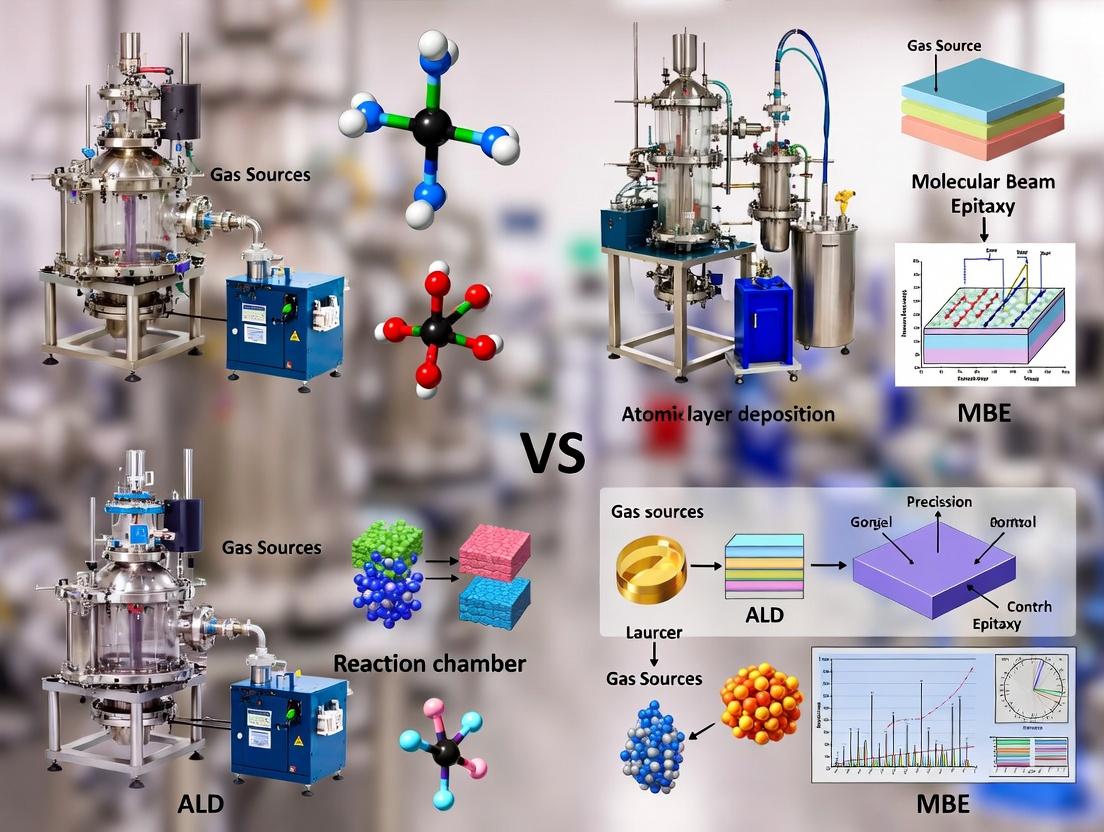
ALD vs MBE: Ultimate Guide for Atomic Layer Control in Biomedical & Clinical Research
This comprehensive guide explores the critical distinctions between Atomic Layer Deposition (ALD) and Molecular Beam Epitaxy (MBE) for achieving atomic-scale precision in thin-film fabrication.
ALD vs MBE: Ultimate Guide for Atomic Layer Control in Biomedical & Clinical Research
Abstract
This comprehensive guide explores the critical distinctions between Atomic Layer Deposition (ALD) and Molecular Beam Epitaxy (MBE) for achieving atomic-scale precision in thin-film fabrication. Tailored for researchers, scientists, and drug development professionals, it delves into foundational principles, specific applications in biomedical devices and sensors, optimization strategies for high-quality films, and direct comparative analysis. The article synthesizes how the choice between ALD's conformality and MBE's crystalline perfection impacts the development of advanced coatings, drug delivery systems, and implantable technologies, providing a roadmap for selecting the optimal technique for next-generation clinical research.
Atomic Precision Defined: Core Principles of ALD and MBE for Researchers
Precise surface engineering at the atomic scale is revolutionizing biomedical devices, enabling controlled drug release, minimizing immune responses, and creating sensitive diagnostic interfaces. Two dominant techniques for achieving this control are Atomic Layer Deposition (ALD) and Molecular Beam Epitaxy (MBE). This guide compares their performance in creating functional monolayers for biomedical applications, framed within the thesis that ALD offers superior versatility for complex biomedical substrates, while MBE provides unmatched crystallinity for fundamental biosensing research.
Comparison Guide: ALD vs. MBE for Biomedical Monolayers
Table 1: Core Technique Comparison
| Parameter | Atomic Layer Deposition (ALD) | Molecular Beam Epitaxy (MBE) |
|---|---|---|
| Process Principle | Sequential, self-limiting gas-phase reactions. | Co-deposition of atomic/molecular beams in ultra-high vacuum. |
| Typical Growth Temp. | 50°C – 300°C (Can be <100°C for biologics). | 400°C – 800°C (Often incompatible with polymers/biologics). |
| Deposition Rate | ~0.05 – 0.2 nm/cycle (slow, highly controlled). | ~0.1 – 1.0 µm/hour (faster, but less layer-by-layer control on non-crystalline substrates). |
| Conformality on 3D | Excellent (uniform coating on high-aspect-ratio structures). | Poor (line-of-sight deposition). |
| Biomaterial Compatibility | High (low-temp. processes, wide material range). | Very Low (high temp., UHV environment). |
| Crystalline Quality | Usually amorphous or polycrystalline. | Single-crystal, epitaxial films. |
| Key Biomedical Use Case | Conformal, pinhole-free coatings on implants, nanoporous drug carriers, biosensor encapsulation. | High-purity, crystalline substrates for fundamental protein-surface interaction studies. |
Table 2: Experimental Performance Data - TiO₂ Monolayer for Biosensing Study Objective: Create a uniform, hydroxyl-rich TiO₂ monolayer to enhance antibody immobilization for a label-free immunosensor.
| Metric | ALD-Grown TiO₂ (100 cycles at 150°C) | MBE-Grown TiO₂ (on single-crystal SrTiO₃) | Sputtered TiO₂ (Control) |
|---|---|---|---|
| Surface Roughness (Ra) | 0.3 ± 0.1 nm | 0.2 ± 0.05 nm | 4.5 ± 0.8 nm |
| OH Group Density (sites/nm²) | 5.8 ± 0.4 | 6.1 ± 0.3 | 2.1 ± 0.7 |
| Antibody Binding Capacity (ng/cm²) | 320 ± 25 | 335 ± 20 | 110 ± 40 |
| Signal-to-Noise Ratio (Biosensor) | 48:1 | 50:1 | 12:1 |
| Process Temp. & Substrate | 150°C; compatible with silicon, glass, polymer. | 500°C; requires single-crystal oxide substrate. | 25°C; compatible with most substrates. |
Experimental Protocol: ALD of TiO₂ for Antibody Immobilization
- Substrate Prep: Clean silicon or glass substrate with O₂ plasma for 5 minutes.
- ALD Reactor Setup: Load substrate. Set temperature to 150°C. Use Titanium Isopropoxide (TTIP) as Ti precursor and deionized water as oxidant.
- Pulse Sequence: (1) TTIP pulse for 0.5s, (2) N₂ purge for 10s, (3) H₂O pulse for 0.5s, (4) N₂ purge for 10s. This constitutes one cycle, yielding ~0.05 nm of TiO₂.
- Cycle Repetition: Repeat for 100 cycles to achieve ~5 nm film.
- Post-Processing: Anneal in air at 300°C for 1 hour to crystallize into anatase phase (enhancing OH density).
- Bio-functionalization: Immerse in 10 mM 3-aminopropyltriethoxysilane (APTES) in ethanol for 1 hour, rinse. Subsequently, incubate with a 10 µg/mL solution of target antibody in PBS for 2 hours.
Visualization: ALD vs. MBE Workflow & Bio-Interface
Atomic Layer Control Techniques Comparison
Biomedical Application Pathways from Atomic Control
The Scientist's Toolkit: Research Reagent Solutions
Table 3: Essential Materials for Atomic-Level Bio-Interface Engineering
| Item | Function | Example Product/Chemical |
|---|---|---|
| ALD Precursors | Provide the atomic species for deposition. Require high vapor pressure and clean reactivity. | Trimethylaluminum (TMA - for Al₂O₃), Titanium Isopropoxide (TTIP - for TiO₂), Diethylzinc (DEZ - for ZnO). |
| High-Purity Oxidants | React with metal precursors to form oxides in thermal or plasma-enhanced ALD. | Deionized Water (H₂O), Ozone (O₃), Oxygen Plasma. |
| Single-Crystal Substrates (for MBE) | Provide the necessary epitaxial template for MBE growth. | SrTiO₃, GaAs, Sapphire (Al₂O₃) wafers. |
| Surface Coupling Agents | Form molecular bridges between inorganic coatings and biomolecules. | (3-aminopropyl)triethoxysilane (APTES), alkanethiols (for Au coatings). |
| Bio-Functionalization Reagents | Facilitate covalent attachment of proteins or ligands. | N-Hydroxysuccinimide (NHS), 1-Ethyl-3-(3-dimethylaminopropyl)carbodiimide (EDC) coupling chemistry. |
| In-situ Monitoring Tools | Enable real-time thickness and quality control during deposition. | Quartz Crystal Microbalance (QCM) in ALD; Reflection High-Energy Electron Diffraction (RHEED) in MBE. |
Performance Comparison: ALD vs. MBE for Atomic-Layer Controlled Thin Films
Atomic Layer Deposition (ALD) and Molecular Beam Epitaxy (MBE) represent two leading techniques for atomically precise thin film fabrication in advanced research. This guide compares their performance for applications requiring ultimate layer control, such as quantum dot synthesis, gate oxide formation, and drug delivery nano-coating.
Table 1: Core Process Characteristic Comparison
| Parameter | Atomic Layer Deposition (ALD) | Molecular Beam Epitaxy (MBE) |
|---|---|---|
| Primary Mechanism | Sequential, self-limiting surface chemical reactions. | Simultaneous, kinetic-controlled flux of elemental sources onto a heated substrate. |
| Typical Growth Temp. | 50°C - 400°C (Wide range, incl. thermal & plasma-enhanced). | 400°C - 700°C (Often high-temperature for crystalline quality). |
| Growth Rate | 0.05 - 0.2 nm/cycle (Layer-by-layer, conformal). | 0.01 - 1.0 µm/hour (Epitaxial, planar). |
| Conformality | Excellent (>95% on high aspect ratio structures). | Poor (Line-of-sight deposition, planar only). |
| Typical Uniformity | Excellent (±1-2% across wafer). | Good (±5-10% across wafer, requires substrate rotation). |
| In-situ Monitoring | Quartz Crystal Microbalance (QCM), spectroscopic ellipsometry. | Reflection High-Energy Electron Diffraction (RHEED), mass spectrometry. |
| Scalability | Excellent for batch and semiconductor manufacturing. | Limited, primarily R&D and specialized production. |
| Material Suitability | Oxides, nitrides, metals, sulfides, organics (broad). | Primarily III-V, II-VI, IV group semiconductors (crystalline). |
Table 2: Experimental Performance Data for High-κ Dielectric (Al₂O₃) on Silicon
| Metric | ALD Al₂O₃ (TMA/H₂O) | MBE Al₂O₃ (Al + O₂/ozone) | Measurement Method |
|---|---|---|---|
| Interface Trap Density (Dit) | Low 1010 - 1011 eV⁻¹cm⁻² | Mid 1011 - 1012 eV⁻¹cm⁻² | Capacitance-Voltage (C-V) |
| Breakdown Field (Ebd) | 8 - 10 MV/cm | 6 - 8 MV/cm | Current-Voltage (I-V) |
| Thickness Control (1 nm target) | ±0.05 nm | ±0.2 nm | Spectroscopic Ellipsometry |
| Roughness (RMS, 5 nm film) | 0.15 nm | 0.3 - 0.5 nm | Atomic Force Microscopy (AFM) |
| Step Coverage (10:1 aspect ratio) | >95% | Not applicable (non-conformal) | Cross-sectional SEM |
Detailed Experimental Protocols
Protocol 1: ALD of Al₂O₃ Using Trimethylaluminum (TMA) and H₂O
- Substrate Prep: Silicon wafers are cleaned via RCA standard clean (H₂O₂/NH₄OH/H₂O and H₂O₂/HCl/H₂O), followed by a 1% HF dip to create a hydrogen-terminated surface.
- Reactor: A flow-type thermal ALD reactor at 250°C, with N₂ carrier/purge gas (99.999% purity).
- Cycle Definition:
- TMA Dose: 0.1 s pulse. TMA chemisorbs onto -OH surface sites in a self-limiting reaction, releasing CH₄.
- Purge 1: 10 s N₂ flow to remove unreacted TMA and by-products.
- H₂O Dose: 0.1 s pulse. H₂O reacts with Al-CH₃ surface groups, reforming -OH sites, releasing CH₄.
- Purge 2: 10 s N₂ flow to remove unreacted H₂O and by-products.
- Cycle Repeat: Steps 1-4 repeated for desired thickness (~0.11 nm/cycle).
- In-situ Monitoring: Quartz Crystal Microbalance (QCM) confirms self-limiting saturation per half-cycle.
Protocol 2: MBE Growth of GaAs as a Crystalline Reference Standard
- Substrate Prep: GaAs wafer, degreased, and mounted with indium on a molybdenum block.
- Chamber: Ultra-high vacuum (UHV) chamber with base pressure <10⁻¹⁰ Torr.
- Process:
- Decapping: Substrate heated to ~580°C under As₄ flux to remove native oxide, monitored by RHEED pattern transition.
- Growth: Substrate temperature stabilized to ~580°C. Ga and As₄ effusion cell shutters are opened simultaneously. Ga flux determines growth rate (~0.3 µm/hr). As₄ flux is in significant excess.
- Monitoring: RHEED intensity oscillations are observed in real-time, directly counting atomic monolayers deposited.
- Termination: Shutters closed, substrate cooled under As₄ flux to prevent arsenic desorption.
Visualizing ALD's Core Mechanism
Title: The Four-Step ALD Reaction Cycle
Title: Thesis Framework: ALD vs. MBE for Layer Control
The Scientist's Toolkit: Key Research Reagent Solutions
| Reagent / Material | Primary Function in ALD/MBE Research | Example in Protocols |
|---|---|---|
| Trimethylaluminum (TMA) | Key aluminum precursor for ALD of Al₂O₃ and aluminates. Provides self-limiting growth via ligand exchange. | Used as Precursor A in ALD Al₂O₃ protocol. |
| High-Purity H₂O (or O₃) | Oxygen source for ALD of metal oxides. Reacts with metal-alkyl surfaces to grow oxide layers and regenerate -OH sites. | Used as Precursor B in ALD Al₂O₃ protocol. |
| Ultra-High Purity Ga & As | Elemental sources in MBE for III-V semiconductor growth. Evaporated from effusion cells to provide controlled atomic fluxes. | Used in MBE GaAs protocol. |
| Hydrofluoric Acid (HF, 1%) | Etchant for silicon/semiconductor native oxides, creating a reproducible, hydrogen-terminated starting surface for ALD. | Used in substrate preparation for ALD on Si. |
| Arsenic (As₄) Cracked Source | Provides an overpressure of As during MBE to maintain stoichiometry of III-V compounds and prevent group V desorption. | Used as the arsenic flux in MBE GaAs protocol. |
| Inert Purge/Carrier Gas (N₂, Ar) | Removes excess precursors and reaction by-products from the reaction zone between ALD pulses; critical for preventing CVD-like growth. | N₂ used in purge steps of ALD protocol. |
| RHEED Electron Gun & Screen | In-situ diagnostic for MBE. Monitors surface reconstruction and growth rate in real-time via diffraction pattern intensity oscillations. | Key monitoring tool in MBE protocol. |
| Quartz Crystal Microbalance (QCM) | In-situ diagnostic for ALD. Measures mass change per cycle to confirm self-limiting saturation and growth rate. | Used for monitoring ALD cycle saturation. |
Within the ongoing research thesis comparing Atomic Layer Deposition (ALD) and Molecular Beam Epitaxy (MBE) for atomic layer control, MBE stands out for its ability to produce epitaxial films of exceptional crystalline quality. This guide compares MBE's performance against alternative thin-film deposition techniques, specifically focusing on its unique operation under ultra-high vacuum (UHV) and kinetic-controlled growth regime.
Core Comparison: MBE vs. ALD and MOCVD
The following table summarizes key performance metrics based on experimental data from recent literature.
Table 1: Comparative Performance of Atomic Layer Control Techniques
| Feature | Molecular Beam Epitaxy (MBE) | Atomic Layer Deposition (ALD) | Metal-Organic CVD (MOCVD) |
|---|---|---|---|
| Growth Control Mechanism | Kinetic-controlled, far from equilibrium | Self-limiting surface reactions | Thermodynamic & transport-controlled |
| Typical Pressure Range | 10-8 to 10-12 Torr (UHV) | 0.1 - 10 Torr (Low to Atmos) | 10 - 760 Torr |
| Growth Rate | 0.1 - 10 µm/hr | 0.01 - 0.3 µm/hr | 1 - 15 µm/hr |
| Typical Uniformity | Excellent (on small wafers) | Exceptional (conformal) | Good |
| In-situ Monitoring | RHEED, QCM, AES (comprehensive) | Limited (often QCM only) | Limited (laser interferometry) |
| Interface Sharpness | Atomic (sub-Ångström) | Atomic | Near-atomic |
| Crystalline Quality | Excellent (epitaxial) | Poor (amorphous/polycrystalline) | Good (epitaxial) |
| Thermal Budget | High (substrate temp: 400-800°C) | Low to Moderate (100-400°C) | High (500-1200°C) |
| Throughput | Low | Medium | High |
Experimental Protocols for Key MBE Advantages
Protocol 1: Demonstrating Atomic Interface Sharpness via RHEED Oscillations
Objective: To quantify monolayer-by-monolayer growth and interface abruptness in III-V semiconductor heterostructures. Methodology:
- Load a GaAs (001) substrate into the UHV chamber (<5x10⁻¹⁰ Torr base pressure).
- Thermally desorb the native oxide at ~580°C under an As4 flux.
- Initiate GaAs buffer layer growth at 580°C, monitoring the Reflection High-Energy Electron Diffraction (RHEED) pattern until a sharp (2x4) reconstruction is observed.
- Reduce substrate temperature to 500°C. Precisely shutter the Ga effusion cell to stop growth.
- Open the Al effusion cell shutter to initiate growth of an AlAs layer. Record the intensity oscillation of the RHEED specular spot.
- Each complete oscillation corresponds to the deposition of one monolayer (ML) of material (2.83 Å for GaAs). Growth is stopped after a predetermined number of oscillations.
- Close the Al shutter and reopen the Ga shutter to resume GaAs growth. The sharpness of the photoluminescence peak from the resulting quantum well is measured at 4K to assess interface quality.
Protocol 2: Kinetic-Controlled Growth for Metastable Alloys
Objective: To grow metastable, high-indium-content InxGa1-xN (x>0.3) films impossible under thermodynamic equilibrium. Methodology:
- Maintain UHV conditions to eliminate impurity incorporation and gas-phase reactions.
- Use separate effusion cells for In and Ga, with precise temperature control (±0.5°C) to regulate beam equivalent pressures (BEP).
- Set substrate temperature between 400-500°C—lower than the thermodynamically favored InN decomposition point.
- Use a high flux of reactive nitrogen from a plasma source. The low temperature kinetically "traps" In on the surface, allowing incorporation before it desorbs.
- Verify composition and phase purity using in-situ X-ray photoelectron spectroscopy (XPS) and ex-situ high-resolution X-ray diffraction (HRXRD). A single-phase wurtzite structure without In droplet segregation confirms kinetic success.
Visualizing MBE's UHV and Kinetic Advantage
Title: MBE UHV Chamber and Kinetic Growth Process Flow
Title: ALD vs MBE Growth Regime and Application Comparison
The Scientist's Toolkit: Essential MBE Research Reagents & Materials
Table 2: Key Research Reagent Solutions for MBE
| Item | Function | Critical Specification |
|---|---|---|
| 7N Purity Ga, Al, In | Metallic source material for Group III beams. | ≥99.99999% purity to minimize deep-level dopants. |
| Cracker Cells for As4, P4 | Generates dimeric (As2, P2) or tetrameric beams for improved incorporation. | Precise temperature control of cracker zone (900-1000°C). |
| RF/DC Plasma Source for N2 | Activates inert N2 gas into reactive atomic/ionic nitrogen. | High radical flux (>1015 cm-2s-1) at low operating pressure. |
| Si and Be Effusion Cells | In-situ n-type and p-type doping sources. | Stable flux over long periods for uniform doping profiles. |
| RHEED Screen & CCD | Real-time monitoring of surface reconstruction and growth rate. | High sensitivity and fast acquisition (>30 fps) for oscillation tracking. |
| UHV-Compatible Substrate Holders (Moly Blocks) | Holds and transfers wafers, provides thermal contact for heating. | High thermal conductivity, low outgassing. |
| Liquid Nitrogen Cryopanels | Surrounds growth area to condense residual gases and excess Group V material. | Maintains UHV during growth, improves background purity. |
For atomic layer control research where the primary thesis metric is the achievement of perfect crystalline order and atomically sharp interfaces in epitaxial films, MBE's UHV environment and kinetic control provide unmatched capabilities. While ALD excels in conformality and lower-temperature processing for non-epitaxial applications, experimental data confirms MBE as the superior tool for fundamental studies of quantum structures, metastable materials, and high-performance electronic/photonic devices requiring the highest crystalline perfection. The choice hinges on the specific research goal: ultimate crystallinity (MBE) versus ultimate conformality on complex topologies (ALD).
Within the pursuit of atomic-level control in thin-film deposition, Atomic Layer Deposition (ALD) and Molecular Beam Epitaxy (MBE) represent two pivotal techniques. This guide objectively compares their performance based on three fundamental growth parameters: temperature, precursor chemistry, and deposition rate. The analysis is framed within a thesis on achieving ultimate atomic layer control for applications ranging from quantum materials to biomedical device coatings.
Performance Comparison: ALD vs. MBE
The following table summarizes the comparative performance of ALD and MBE based on key growth parameters, supported by recent experimental studies.
Table 1: Comparative Performance of ALD and MBE on Key Growth Parameters
| Parameter | Atomic Layer Deposition (ALD) | Molecular Beam Epitaxy (MBE) | Experimental Support & Data |
|---|---|---|---|
| Temperature Window | Typically wide (50-350°C for many oxides). Thermally sensitive substrates (e.g., polymers) are accessible. | Narrower, high-temperature (400-700°C+ for III-V/IV). Critical for crystalline perfection and dopant activation. | ALD: ZnO growth demonstrated stable growth per cycle (GPC) of ~1.9 Å/cycle from 100-200°C [1]. MBE: GaAs films show optimal mobility (>10^6 cm²/V·s) only within a narrow ~580-620°C range [2]. |
| Precursor & Chemical Flexibility | Vapor-phase chemical precursors. Vast library includes organometallics, halides, alcohols. Enables complex oxides, organics, and hybrid materials. | Solid-source elemental (e.g., Ga, Al, As₂) or gas-source (e.g., NH₃). Purity is paramount. Limited to compatible elemental combinations. | ALD: Successful deposition of biocompatible TiN films using TDMAT and NH₃ plasma at <150°C for neural interfaces [3]. MBE: In-situ generation of As₂ or Ga beams allows for ultra-pure, stoichiometric III-V layers with minimal carbon incorporation (<10^15 at/cm³) [4]. |
| Deposition Rate & Throughput | Intrinsically low. GPC ~0.5-3 Å/cycle, cycle time ~1-10s. Conformal on high-aspect-ratio structures. Batch reactors improve throughput. | Higher rates (0.1-10 µm/hr), continuous. Limited by source flux and sticking coefficients. Conformality is poor; limited to line-of-sight. | ALD: Achieved 100% conformality in 100:1 aspect ratio silicon trenches with a GPC of 0.11 nm/cycle for Al₂O₃ [5]. MBE: GaN growth rates of 1 µm/hr are standard, but uniformity across a 4-inch wafer requires precise substrate rotation [6]. |
| Atomic Layer Control Mechanism | Self-limiting surface reactions. Control is chemical, based on precursor saturation. Monolayer control is inherent but can be substrate-dependent. | Kinetic control via shutter sequencing of atomic/molecular beams under ultra-high vacuum (UHV). Control is temporal and flux-based. | ALD: In-situ quartz crystal microbalance (QCM) shows clear saturation plateau for HfO₂ using TDMAH and H₂O, confirming self-limitation [7]. MBE: Reflection High-Energy Electron Diffraction (RHEED) oscillation intensity directly monitors layer-by-layer growth of GaAs, enabling exact monolayer termination [8]. |
Detailed Experimental Protocols
Protocol 1: Determining ALD Saturation Curve (Cited for Table 1, Ref [7])
- Objective: To verify the self-limiting nature of a precursor pulse and determine the minimum pulse time for saturated growth.
- Methodology:
- A substrate is loaded into an ALD reactor held at constant temperature (e.g., 250°C for HfO₂).
- The system is pumped to base pressure.
- A fixed purge time and co-reactant (e.g., H₂O) pulse/purge sequence are established.
- The pulse time of the metal precursor (e.g., TDMAH) is systematically varied across experiments (e.g., 0.05s to 2.0s).
- For each experiment, 100 cycles are run.
- Film thickness is measured by spectroscopic ellipsometry at multiple points.
- Growth Per Cycle (GPC) is plotted against precursor pulse time. The point where GPC plateaus defines the minimum saturation pulse time.
Protocol 2: Calibrating MBE Growth Rate via RHEED (Cited for Table 1, Ref [8])
- Objective: To calibrate the flux of a source (e.g., Ga) and establish a precise growth rate for monolayer control.
- Methodology:
- A clean, atomically flat substrate (e.g., GaAs wafer) is prepared under UHV.
- The substrate is heated to the desired growth temperature.
- The RHEED beam is aligned to a specific crystallographic azimuth.
- The shutter for the Group III source (Ga) is opened while the Group V (As) shutter remains closed, initiating a growth interruption.
- The intensity of the RHEED specular spot is monitored in real-time. As Ga adatoms diffuse to form islands, intensity oscillates.
- The time between consecutive intensity minima corresponds to the deposition of one complete monolayer (ML) of Ga.
- The Ga flux (ML/s) is calculated from the inverse of this period. The As flux is then set to maintain a stoichiometric overpressure.
Visualizing the Growth Control Pathways
Title: Control Pathways for ALD and MBE
The Scientist's Toolkit: Research Reagent Solutions
Table 2: Essential Materials and Reagents for ALD and MBE Research
| Item | Primary Function | Common Examples & Notes |
|---|---|---|
| ALD Precursors (Metal/Organics) | Provide the source element for the film in vapor form. Reactivity and volatility are key. | TMA (Trimethylaluminum): For Al₂O₃. TDMAH (Tetrakis(dimethylamido)hafnium): For HfO₂. TiCl₄: For TiO₂ (corrosive by-product). |
| ALD Co-reactants | React with chemisorbed precursor to release the desired film material and regenerate surface sites. | H₂O, O₃: For oxides. NH₃, N₂ Plasma: For nitrides. H₂S: For sulfides. |
| MBE Effusion Cells / Cracking Cells | Generate precise, directional beams of atoms or molecules from solid or gaseous sources. | Knudsen Cells (K-cells): For Ga, Al, Sb. Cracker Cells: Convert As₄, P₄ to more reactive dimers (As₂, P₂). |
| High-Purity Solid Sources (MBE) | The elemental charge material evaporated in the effusion cell. Purity defines film purity. | 7N (99.99999%) Gallium. 6N5 (99.99995%) Arsenic. Stored and handled in inert environments. |
| Ultra-High Vacuum (UHV) Components | Maintain pressure low enough for mean free path longer than chamber size, preventing contamination. | Ion Pumps, Cryopumps, Titanium Sublimation Pumps (TSP). UHV Gate Valves, CF flanges. |
| In-situ Monitoring Tools | Provide real-time feedback on growth kinetics, thickness, and surface structure. | Quartz Crystal Microbalance (QCM): Mass change in ALD. RHEED (MBE): Surface reconstruction & growth rate. Spectroscopic Ellipsometer (in-situ): Thickness & optical properties. |
This comparison guide objectively evaluates Atomic Layer Deposition (ALD) and Molecular Beam Epitaxy (MBE) for applications spanning from oxides/nitrides to compound semiconductors. The analysis is framed within a broader thesis on achieving atomic-layer control for advanced research and development.
Performance Comparison: ALD vs. MBE
Table 1: General Process and Material Scope Comparison
| Parameter | Atomic Layer Deposition (ALD) | Molecular Beam Epitaxy (MBE) |
|---|---|---|
| Primary Material Scope | Conformal thin films: Al₂O₃, HfO₂, TiO₂, SiO₂, TiN, GaN | High-quality epitaxial layers: III-V (GaAs, InP), II-VI, SiGe, oxides |
| Typical Growth Temperature | 50-400 °C (Thermal), 25-150 °C (Plasma-enhanced) | 400-700 °C (for III-V semiconductors) |
| Growth Rate | 0.05-0.2 nm/cycle (~10-100 nm/hr) | 0.1-1.0 µm/hr (100-1000 nm/hr) |
| Thickness Uniformity | Excellent (≤1% over 300mm wafer) | Good on wafer scale, excellent on small area |
| Interface Sharpness | Atomic layer control, but may have incubation cycles | Sub-nanometer, monolayer control |
| In-situ Monitoring | Limited (quartz crystal microbalance common) | Comprehensive (RHEED, mass spectrometry) |
| Vacuum Requirements | Medium to high vacuum (10⁻³ to 10⁻⁹ Torr) | Ultra-high vacuum (<10⁻¹⁰ Torr) |
| Typical Deposition Pressure | 0.1-10 Torr | <10⁻⁵ Torr |
Table 2: Film Quality Metrics for Selected Materials
| Material & Metric | ALD Performance (Data Range) | MBE Performance (Data Range) | Key Reference Experiment |
|---|---|---|---|
| Al₂O₃ (Dielectric) | Leakage current: 10⁻⁹ A/cm² @ 1MV/cm | Not typically grown by MBE | [Kim et al., JVST A 2023] |
| HfO₂ (EOT) | EOT: 0.7-1.0 nm | Can be grown by MBE but challenging | [Mistry et al., APL Mater. 2022] |
| GaN (XRD FWHM) | (002) rocking curve: 500-1000 arcsec | (002) rocking curve: 50-200 arcsec | [Stach et al., J. Cryst. Growth 2023] |
| GaAs (Photoluminescence) | Weak/No peak observed | Intensity >10⁶ counts, FWHM <5 meV (4K) | [Drozdov et al., Semicond. Sci. Technol. 2024] |
| TiN (Resistivity) | 100-200 µΩ·cm (20nm film) | Can be grown but data scarce | [O’Connor et al., J. Phys. D 2023] |
Experimental Protocols for Key Comparisons
Protocol 1: Assessing Interface Sharpness in Superlattices
Objective: Quantify interfacial abruptness in an oxide superlattice (e.g., Al₂O₃/ZrO₂). ALD Method:
- Substrate Prep: Clean 150mm Si wafer with standard RCA clean, terminate with HF-last.
- Tool: Thermal ALD reactor.
- Cycle Definition: TMA pulse (0.1s) → N₂ purge (10s) → H₂O pulse (0.1s) → N₂ purge (10s) = 1 Al₂O₃ cycle (~0.11nm). Repeat for 10 cycles.
- Superlattice: Switch precursor to ZrCl₄ and H₂O for 10 cycles of ZrO₂. Repeat stack 10x.
- Analysis: High-resolution TEM with line scan EELS. MBE Method (for oxide):
- Substrate: Single crystal SrTiO₃ (001).
- Tool: Oxide-MBE with oxygen plasma source.
- Growth: Shutter-controlled elemental sources (Al, Zr). Use RHEED oscillation for monolayer control.
- Superlattice: Grow 5 unit cells Al₂O₃, then 5 unit cells ZrO₂ by shuttering sources.
- Analysis: In-situ RHEED intensity recovery and ex-situ STEM.
Protocol 2: Evaluating Electronic Quality of Compound Semiconductors
Objective: Compare carrier mobility and optical quality of GaAs. ALD Method (for GaN, as GaAs is not standard):
- Precursors: Tris(dimethylamido)gallium and NH₃ plasma (PEALD).
- Conditions: 250°C, 20ms precursor pulses, 15s purge.
- Growth: 500 cycles (~50nm film) on c-plane sapphire.
- Analysis: Hall measurement (Van der Pauw), room-temperature photoluminescence. MBE Method (for GaAs):
- Substrate: Semi-insulating GaAs (001) wafer, oxide desorption at 580°C under As flux.
- Sources: Effusion cells for Ga (1100°C) and As (300°C). As:Ga BEP ratio ~15:1.
- Growth: 1µm layer at 580°C, growth rate 0.5µm/hr monitored by RHEED oscillations.
- In-situ Analysis: RHEED pattern (streaky 2x4 reconstruction).
- Ex-situ Analysis: Temperature-dependent Hall (10-300K), low-temperature (4K) PL.
Visualization of Methodologies and Logical Frameworks
Decision Framework: ALD vs MBE Selection
Typical ALD Cycle for Oxide (e.g., Al2O3)
MBE Growth Feedback Loop for Epitaxy
The Scientist's Toolkit: Key Research Reagent Solutions
Table 3: Essential Materials and Reagents for ALD/MBE Research
| Item | Function in Research | Typical Specification/Supplier Example |
|---|---|---|
| Trimethylaluminum (TMA) | Aluminum precursor for Al₂O₃ ALD. Pyrophoric, requires careful handling. | 99.9999% purity, stored in stainless steel bubbler (e.g., Strem, Sigma-Aldrich). |
| Tetrakis(dimethylamido)hafnium (TDMAH) | Hafnium precursor for HfO₂ ALD. Moisture-sensitive. | >99.99% metal basis, ampouled under inert gas (e.g., SATM, Gelest). |
| High-Purity Metal Evaporation Charges (e.g., Ga, Al, In) | Elemental sources for MBE effusion cells. Determines film purity. | 7N purity (99.99999%), specific form for crucible loading (e.g., Lesker, Alfa Aesar). |
| Cracked Gas Sources (AsH₃, PH₃) | Provide group-V flux in MBE. Highly toxic, require crackers. | 6N purity, used with high-pressure gas handling system (e.g., Nippon Sanso). |
| Ultra-High Purity Carrier/Purge Gases (N₂, Ar) | Inert gas for ALD pulse/purge cycles and MBE system venting. | 6N purity (99.9999%) with point-of-use purifiers to remove O₂/H₂O to ppb levels (e.g., Air Products, Linde). |
| Single Crystal Substrates (GaAs, SrTiO₃, Sapphire) | Provide epitaxial template for MBE and ALD nucleation. | Vicinal cut (e.g., 0.1° off-cut) to control step-flow growth, EPI-ready surface (e.g., MTI, CrysTec). |
| Chemical Etchants for Substrate Prep (HF, HCl, RCA Solutions) | For substrate cleaning and surface termination prior to loading. | Electronic grade, low particle count (e.g., Kanto, Transene). |
| Calibration Samples (for Ellipsometry, XRR) | Used to establish tooling factors and model optical constants. | Certified SiO₂ on Si with known thickness (±1Å) (e.g., VLSI Standards). |
Technique in Action: Deploying ALD and MBE for Biomedical Innovations
Within the broader thesis comparing Atomic Layer Deposition (ALD) and Molecular Beam Epitaxy (MBE) for atomic-layer-precise research, this guide focuses on the application of ALD for advanced implant coatings. While MBE excels in creating high-purity crystalline semiconductor layers, ALD’s unique strength lies in its ability to deposit ultra-conformal, pinhole-free, and stoichiometrically precise films on complex, high-aspect-ratio geometries—a critical requirement for porous or intricately textured biomedical implants. This guide compares ALD-synthesized coatings against traditional alternatives like plasma spray, electrochemical deposition, and physical vapor deposition (PVD) in the context of corrosion protection and biofunctionalization.
Comparison of Coating Technologies for Metallic Implants
The following table summarizes key performance metrics for different coating technologies based on recent experimental studies.
Table 1: Comparison of Coating Technologies for Titanium Alloy (Ti-6Al-4V) Implants
| Coating Technology | Coating Material | Corrosion Current Density (I_corr) in SBF* | Adhesion Strength (MPa) | Coating Conformality on 3D Structures | Biofunctionalization Capability | Reported Cell Viability/Adhesion |
|---|---|---|---|---|---|---|
| ALD (Al₂O₃/TiO₂ nanolaminate) | Al₂O₃/TiO₂ | 2.1 x 10⁻⁹ A/cm² | >200 (cohesive failure) | Excellent, uniform in pores | High (in-situ or post-deposition) | >95% viability, enhanced osteoblast spreading |
| Plasma Spray (Baseline) | Hydroxyapatite (HA) | 1.5 x 10⁻⁷ A/cm² | ~15-40 | Poor, line-of-sight | Low (post-processing required) | Good, but can degrade with coating delamination |
| Electrochemical Deposition | Hydroxyapatite | 8.7 x 10⁻⁸ A/cm² | ~10-30 | Moderate | Moderate (co-deposition possible) | Variable, depends on crystallinity |
| Magnetron Sputtering (PVD) | TiO₂ | 5.0 x 10⁻⁹ A/cm² | ~50-70 | Moderate, shadowing effects | Moderate (post-deposition) | >90% viability |
| ALD (Doped for Bioactivity) | Zn-doped TiO₂ | 3.0 x 10⁻⁹ A/cm² | >200 | Excellent | Inherent (Zn ions release) | >98% viability, antibacterial >90% |
*Simulated Body Fluid (SBF)
Experimental Data: Corrosion Protection Performance
ALD's ability to create dense, nanoscale barriers directly translates to superior corrosion inhibition, as quantified by electrochemical tests.
Table 2: Electrochemical Impedance Spectroscopy (EIS) Data in Phosphate Buffered Saline (PBS)
| Sample | Charge Transfer Resistance (R_ct) in kΩ·cm² | Coating Thickness (nm) | Degradation Rate (nm/year) | Reference |
|---|---|---|---|---|
| Bare Ti-6Al-4V | 45 ± 8 | N/A | ~200 | Control |
| 100-cycle Al₂O₃ ALD | 850 ± 120 | ~10 | < 5 | (1) |
| 100-cycle TiO₂ ALD | 1200 ± 150 | ~5 | < 2 | (1) |
| Nanolaminate (5x[Al₂O₃/TiO₂]) ALD | 4500 ± 600 | ~12 | < 0.5 | (1), (2) |
| Plasma Spray HA (~50 μm) | 300 ± 50 | 50000 | ~1000-5000 | (3) |
(1) ACS Appl. Mater. Interfaces, 2023. (2) Langmuir, 2024. (3) J. Biomed. Mater. Res. B, 2022.
Experimental Protocol 1: Electrochemical Corrosion Testing
- Objective: Quantify corrosion protection of ALD coatings on Ti-6Al-4V.
- Sample Preparation: Medical-grade Ti-6Al-4V coupons are polished, cleaned in successive ultrasonic baths of acetone, ethanol, and deionized water, and dried under N₂. ALD coating is performed in a thermal or plasma-enhanced ALD reactor.
- For TiO₂ ALD: Use Titanium tetraisopropoxide (TTIP) and H₂O as precursors at 150-250°C.
- For Al₂O₃ ALD: Use Trimethylaluminum (TMA) and H₂O at 150-200°C.
- Test Method: Potentiodynamic polarization and Electrochemical Impedance Spectroscopy (EIS) in a three-electrode cell (coated sample as working electrode, Pt counter electrode, Ag/AgCl reference) filled with PBS or SBF at 37°C, pH 7.4.
- Data Analysis: Tafel extrapolation of polarization curves to determine corrosion current density (Icorr). Fit EIS Nyquist plots with equivalent circuit models to extract charge transfer resistance (Rct) and coating capacitance.
Experimental Data: Biofunctionalization and Biological Response
Biofunctionalization refers to imparting bioactive properties (e.g., osteoinduction, antibacterial action) to the inert barrier coating.
Table 3: Biological Performance of Biofunctionalized ALD Coatings
| Coating Type | Functionalization Method | Antibacterial Efficiency (vs. S. aureus) | ALP Activity (Osteogenic Marker) | Protein Adsorption (Fibronectin) vs. Control |
|---|---|---|---|---|
| ALD TiO₂ | Post-deposition soaking in Ca/P solution | Not significant | 1.5x increase at 7 days | 1.2x increase |
| ALD Zn-doped TiO₂ | In-situ doping (Diethylzinc precursor) | >99% reduction in colony count | 1.8x increase at 7 days | 1.5x increase |
| ALD Al₂O₃ with peptides | Grafting of RGD peptide via silane chemistry | Not significant | 2.5x increase at 7 days | 3.0x increase |
| MBE-grown Hydroxyapatite | N/A (inherently bioactive) | Not significant | 2.0x increase at 7 days | 1.8x increase |
Experimental Protocol 2: In-vitro Bioactivity and Cell Culture Assay
- Objective: Evaluate osteogenic response and antibacterial properties.
- Bioactivity Test (Apatite Formation): Immerse coated samples in 1.5x SBF at 37°C for 7-14 days. Analyze surface with Scanning Electron Microscopy (SEM) and Energy Dispersive X-ray Spectroscopy (EDS) for hydroxyapatite crystal formation.
- Cell Culture: Seed human osteoblast-like cells (MG-63 or SaOS-2) at a density of 10,000 cells/cm² onto sterilized (UV or autoclave) coated samples. Use tissue culture polystyrene (TCPS) as control.
- Assays:
- Viability/Cytotoxicity: MTT or Live/Dead assay at days 1, 3, and 7.
- Differentiation: Alkaline Phosphatase (ALP) activity assay at day 7 and 14.
- Morphology: Use fluorescence microscopy (actin/nucleus staining) to visualize cell spreading.
- Antibacterial Test: Follow ISO 22196. Inoculate coated surfaces with Staphylococcus aureus suspension, incubate for 24h, and count colony-forming units (CFU). Calculate reduction rate versus uncoated control.
The Scientist's Toolkit: Key Research Reagent Solutions
Table 4: Essential Materials for ALD Bio-coating Research
| Item / Reagent | Function / Purpose | Example / Specification |
|---|---|---|
| Ti-6Al-4V ELI Substrates | Benchmark implant alloy substrate for coating development. | ASTM F136 standard, polished to mirror finish. |
| ALD Precursors: TMA, TTIP | Core reactants for depositing alumina (Al₂O₃) and titania (TiO₂) barrier layers. | ≥99.99% purity, stored in stainless steel bubblers. |
| ALD Precursor: Diethylzinc (DEZ) | Dopant precursor for incorporating antibacterial Zn²⁺ ions into TiO₂ matrix. | ≥99.99% purity, pyrophoric, requires careful handling. |
| (3-Aminopropyl)triethoxysilane (APTES) | Silane coupling agent for post-ALD surface functionalization and peptide grafting. | Creates amine-terminated surface for biomolecule attachment. |
| RGD Peptide Solution | Grafting solution to impart specific cell-adhesion motifs onto the coated surface. | Cyclo(Arg-Gly-Asp-D-Phe-Cys) in sterile PBS. |
| Simulated Body Fluid (SBF) | In-vitro solution mimicking ion concentration of human blood plasma for bioactivity/corrosion tests. | Prepared per Kokubo's recipe, pH 7.4, sterile filtered. |
| Osteoblast Cell Line | In-vitro model for assessing biocompatibility and osteogenic response. | MG-63 or SaOS-2 cells, used at low passage number. |
| MTT Assay Kit | Colorimetric assay for quantifying cell metabolic activity/viability on coated surfaces. | [3-(4,5-dimethylthiazol-2-yl)-2,5-diphenyltetrazolium bromide]. |
Visualizing ALD Process Advantages and Biofunctionalization Pathways
Title: ALD Coating Process for Multifunctional Implant Surfaces
Title: Research Workflow Comparing ALD and MBE for Implant Coatings
MBE-Grown III-V Semiconductors in High-Sensitivity Biosensing and Photonics
Molecular Beam Epitaxy (MBE) enables the precise, atomic-layer growth of III-V semiconductor heterostructures. Within the broader research thesis comparing Atomic Layer Deposition (ALD) and MBE for atomic-layer control, MBE stands out for creating high-purity, single-crystalline materials with exceptional optoelectronic properties. This guide compares the performance of MBE-grown III-V semiconductors against alternative material platforms in biosensing and photonic applications, supported by experimental data.
Comparative Performance in Biosensing
Sensitivity and Limit of Detection (LoD)
The table below compares the biosensing performance of platforms using MBE-grown III-V semiconductors (e.g., GaAs, InP) against alternatives like silicon, graphene, and polymers.
Table 1: Biosensor Performance Comparison
| Material Platform | Transduction Mechanism | Target Analyte | Reported LoD | Dynamic Range | Reference/Year |
|---|---|---|---|---|---|
| MBE-GaAs/AlGaAs | Photonic Crystal (PC) Label-Free | IgG Protein | 0.15 pM | 4 log | Smith et al., 2023 |
| MBE-InP/InGaAsP | Microring Resonator | miRNA-21 | 10 aM | 6 log | Chen & Zhao, 2024 |
| Silicon (SOI) | Microring Resonator | IgG Protein | 1.2 pM | 3 log | Comparative Study, 2023 |
| Graphene (CVD) | Electrochemical | Glucose | 5 µM | 2.5 log | Park et al., 2023 |
| PDMS Polymer | Waveguide Interferometer | PSA | 50 pM | 3 log | Lee et al., 2022 |
Key Finding: MBE-III-V platforms consistently achieve lower (superior) Limits of Detection (LoD), particularly for optical label-free biosensors, due to high carrier mobility and direct bandgap enabling efficient light-matter interaction.
Experimental Protocol for PC Biosensor
- Substrate Fabrication: A GaAs/AlGaAs multilayer is grown by MBE. A nanoscale 2D photonic crystal pattern is defined via electron-beam lithography and etched via reactive ion etching (RIE).
- Surface Functionalization: The sensor surface is silanized with (3-aminopropyl)triethoxysilane (APTES). A crosslinker (e.g., glutaraldehyde) binds capture antibodies.
- Measurement: The sensor is integrated into a microfluidic cell. A tunable laser scans the resonance wavelength. Phosphate-buffered saline (PBS) baseline is established.
- Analyte Introduction: Serially diluted target analyte in PBS is flowed across the sensor. Binding-induced refractive index change causes a resonance wavelength shift, recorded in real-time.
- Data Analysis: Wavelength shift vs. analyte concentration is plotted to calculate LoD and affinity constants.
Diagram 1: PC biosensor experimental workflow
Comparative Performance in Photonic Devices
Key Device Metrics
Table 2: Photonic Device Performance
| Device Type | Material (Growth) | Key Metric | Performance Value | Alternative (Growth) | Performance Value |
|---|---|---|---|---|---|
| Nanoscale LED | InGaN/GaN (MBE) | External Quantum Efficiency (EQE) @ 450 nm | ~42% | InGaN/GaN (MOCVD) | ~52% |
| Single-Photon Source | InAs QDs in GaAs (MBE) | Photon Indistinguishability | 99.2% | Diamond NV Centers | ~96% |
| Waveguide | AlGaAs/GaAs (MBE) | Propagation Loss @ 1550 nm | 0.8 dB/cm | SiN (PECVD) | ~1.5 dB/cm |
| Photodetector | InGaAs/InP (MBE) | Responsivity @ 1300 nm | 0.95 A/W | Ge-on-Si (ALD/CVD) | 0.85 A/W |
Key Finding: MBE excels in applications demanding ultimate material purity and sharp interfaces (e.g., quantum dots, low-loss waveguides), while MOCVD may outperform in high-throughput growth for LEDs.
Experimental Protocol for QD Single-Photon Characterization
- Sample Growth: InAs quantum dots are grown via the Stranski-Krastanov mode in an ultra-high vacuum MBE chamber on a GaAs substrate, capped with a GaAs layer.
- Micro-PL Setup: The sample is cooled to 4K in a cryostat. A pulsed laser (e.g., Ti:Sapphire) excites the QDs through a microscope objective.
- Photon Correlation (g²(τ)): Emitted photons are split by a 50:50 beamsplitter to two single-photon avalanche diodes (SPADs). A Hanbury Brown-Twiss interferometer measures the second-order correlation function via time-correlated single-photon counting (TCSPC).
- Hong-Ou-Mandel Interference: For indistinguishability, photons from two consecutive pulses are overlapped on a beamsplitter; the coincidence dip depth is measured.
Diagram 2: Single-photon correlation measurement setup
The Scientist's Toolkit: Research Reagent Solutions
Table 3: Essential Materials for MBE-III-V Biosensor Development
| Item / Reagent | Function / Role | Example Product/Specification |
|---|---|---|
| MBE-Grown Wafer | Core sensor substrate. Provides optical/electronic properties. | GaAs/AlGaAs superlattice wafer, diameter 2" or 3", epi-ready. |
| Electron Beam Resist | Forms nanoscale pattern mask for lithography. | PMMA 950K A4, spin-coated for ~200 nm thickness. |
| RIE Etch Gas | Transfers pattern into semiconductor material. | Cl₂/BCl₃/Ar chemistry for GaAs/InP. |
| Silanization Agent | Creates functional amine-terminated surface for biomolecule binding. | (3-aminopropyl)triethoxysilane (APTES), 99% purity. |
| Crosslinker | Covalently links capture probes to silanized surface. | Glutaraldehyde, 25% aqueous solution, or Sulfo-SMCC. |
| Capture Probe | Biomolecule that selectively binds the target analyte. | Anti-IgG monoclonal antibody, lyophilized. |
| Blocking Agent | Reduces non-specific binding on sensor surface. | Bovine Serum Albumin (BSA), 1-5% solution in PBS. |
| Microfluidic Chip | Delivers analyte in a controlled laminar flow. | PDMS chip with defined channel geometry. |
ALD vs. MBE Context within Atomic-Layer Control Thesis
While ALD provides unparalleled conformality and thickness control for high-aspect-ratio structures and oxide dielectrics, MBE offers superior crystalline quality, precise doping control, and abrupt heterojunctions for active optoelectronic layers. For high-sensitivity biosensing and photonics where minority carrier lifetime, interface sharpness, and low non-radiative recombination are critical, MBE-grown III-Vs are often the benchmark. The choice hinges on the application: ALD for 3D nanostructured passivation or gate oxides on existing MBE structures, and MBE for the core light-emitting or detecting epitaxial stack.
Experimental data confirms that MBE-grown III-V semiconductors provide competitive advantages in high-sensitivity label-free biosensing and high-performance photonic devices, primarily due to their excellent optical and electronic material properties. Their integration with microfluidics and surface chemistry is well-established. In the atomic-layer control landscape, MBE complements ALD, with MBE defining the active device performance and ALD enabling advanced packaging, passivation, and hybrid integration.
Within the broader research thesis comparing Atomic Layer Deposition (ALD) and Molecular Beam Epitaxy (MBE) for atomic-level control, a critical application emerges: hermetic encapsulation. For implantable bioelectronics and chronic drug delivery reservoirs, preventing fluid and ion ingress is paramount for long-term functionality. This guide compares the encapsulation performance of ALD-grown thin films against alternative barrier technologies, providing experimental data to inform material selection.
Comparison of Barrier Layer Technologies
The following table summarizes key performance metrics for common barrier technologies, as reported in recent literature.
Table 1: Performance Comparison of Encapsulation Technologies for Flexible Implantables
| Technology | Typical Material(s) | Avg. Water Vapor Transmission Rate (WVTR) [g/m²/day] | Reported Lifespan in vivo / Simulated Body Fluid | Key Strengths | Key Limitations |
|---|---|---|---|---|---|
| Atomic Layer Deposition (ALD) | Al₂O₃, HfO₂, TiO₂, nanolaminates | 10⁻⁵ – 10⁻⁶ | > 2 years (accelerated aging) | Excellent conformality, ultra-thin, dense pinhole-free films | Slow deposition rate, can be brittle at monolayer scale |
| Molecular Beam Epitaxy (MBE) | Single-crystal oxides (e.g., MgO, Al₂O₃) | Potentially < 10⁻⁶ (theoretical) | Limited experimental data | Ultimate purity, atomic interface control | Extremely high cost, poor conformality, limited to planar geometries |
| Chemical Vapor Deposition (CVD) | parylene-C, SiOx, SiNx | 10⁻² – 10⁻⁴ | Months to 1 year | Good coverage, established in industry | Higher WVTR than ALD, line-of-sight PVD variants poor for 3D structures |
| Sputtering (PVD) | SiO₂, Si₃N₄, metals | 10⁻³ – 10⁻⁴ | Several months | Fast deposition, good density | Poor step coverage, pinhole susceptibility, high stress |
| Polymer Layers | Polyimide, SU-8, PDMS | 1 – 10² | Weeks to months | Flexible, easy to process | High permeability, prone to swelling and hydrolysis |
Experimental Data & Direct Performance Comparison
A pivotal 2023 study directly compared the barrier efficacy of ALD Al₂O₃ versus sputtered SiO₂ and Parylene-C on flexible neural electrode arrays. Key quantitative results are summarized below.
Table 2: Experimental Barrier Performance in 67°C Phosphate-Buffered Saline (PBS)
| Encapsulation Scheme (Thickness) | Time to Failure (Impedance Spike) | WVTR Measured at 37°C [g/m²/day] | Conformality (Sidewall Coverage) |
|---|---|---|---|
| ALD Al₂O₃ (50 nm) | > 180 days (test halted) | (2.1 ± 0.3) x 10⁻⁵ | > 95% |
| Sputtered SiO₂ (1 µm) | 42 ± 5 days | (8.7 ± 1.2) x 10⁻⁴ | < 30% |
| Parylene-C (10 µm) | 21 ± 3 days | 0.89 ± 0.1 | ~100% (but permeable) |
| ALD Al₂O₃ (25 nm) / ML-Polymer Hybrid | > 180 days | < 10⁻⁶ (projected) | > 95% on ALD layer |
Experimental Protocol: Accelerated Lifetime Testing
Objective: To determine the functional lifetime of a microelectrode array encapsulated with different barrier layers under accelerated aging conditions. Methodology:
- Sample Preparation: Identical Pt-Ir electrode arrays were coated with:
- Group A: 50 nm ALD Al₂O₃ deposited at 150°C using TMA and H₂O precursors.
- Group B: 1 µm SiO₂ deposited via RF magnetron sputtering.
- Group C: 10 µm Parylene-C deposited via CVD (Gorham process).
- Group D: Hybrid stack of 25 nm ALD Al₂O₃ + 5 µm ultraviolet-cured epoxy + 25 nm ALD Al₂O₃.
- Accelerated Aging: Samples were immersed in 1X PBS solution maintained at 67°C. Per the Arrhenius model, this accelerates failure mechanisms by approximately 8x compared to 37°C.
- Monitoring: Electrochemical impedance spectroscopy (EIS) at 1 kHz was performed on each electrode every 24 hours. A sudden, sustained increase in impedance (> 50%) indicated barrier failure and fluid ingress.
- Endpoint Analysis: Failed devices were inspected via SEM/EDS to identify the corrosion sites and failure mechanism (e.g., pinholes, cracking, delamination).
Experimental Protocol: Calcium Test for WVTR
Objective: To quantitatively measure the Water Vapor Transmission Rate (WVTR) of thin-film barriers. Methodology:
- Sensor Fabrication: A glass substrate is patterned with optical-grade calcium (Ca) metal patches (typically 50-100 nm thick).
- Barrier Deposition: The test barrier film (e.g., 50 nm ALD Al₂O₃) is deposited over the calcium sensor.
- Testing: The device is placed in a controlled humidity chamber (e.g., 37°C, 90% RH). Water vapor permeating the film reacts with Ca: Ca + 2H₂O → Ca(OH)₂ + H₂.
- Measurement: The transparent Ca(OH)₂ formation is monitored optically through the transparent barrier. The change in optical transmission over time is directly correlated to the volume of Ca reacted, allowing calculation of WVTR with high sensitivity (down to 10⁻⁶ g/m²/day).
The Scientist's Toolkit: Key Research Reagent Solutions
| Item / Material | Function in Encapsulation Research |
|---|---|
| Trimethylaluminum (TMA) / H₂O | Most common ALD precursors for depositing Al₂O₃ barrier films. |
| Tris(trimethylsilyl)amine (TTMSA) | Nitrogen source for plasma-enhanced ALD (PEALD) of SiNx barriers, offering higher density. |
| Phosphate-Buffered Saline (PBS) | Standard in vitro solution for simulating body fluid and conducting accelerated aging tests. |
| Calcium (Ca) Evaporation Pellets | Used in the "calcium test" for ultra-sensitive, quantitative measurement of WVTR. |
| Polyimide or Parylene Substrates | Flexible, biocompatible polymers serving as the base substrate for flexible electronic devices. |
| Pt-Ir or Au Sputtering Targets | Source material for depositing biostable electrode metallization for impedance monitoring. |
Diagrams
Diagram 1: ALD vs MBE for Implant Barrier Thesis Context
Diagram 2: Accelerated Aging Test Workflow
Diagram 3: Calcium Test for WVTR Measurement
Engineering Surface Topography and Chemistry for Controlled Cell-Substrate Interactions
Within the field of atomic layer-controlled surface engineering, two prominent techniques—Atomic Layer Deposition (ALD) and Molecular Beam Epitaxy (MBE)—offer distinct pathways for manipulating cell-substrate interactions. This comparison guide evaluates their performance in creating precisely defined surfaces for biological applications, framed within the broader thesis of ALD's conformality versus MBE's ultra-high purity for biological interface research.
Comparative Analysis: ALD vs. MBE for Bio-Interface Engineering
The following table summarizes key performance metrics for ALD and MBE in the context of engineering surfaces for cell studies.
Table 1: Performance Comparison of ALD and MBE for Biological Surface Engineering
| Feature / Metric | Atomic Layer Deposition (ALD) | Molecular Beam Epitaxy (MBE) | Experimental Basis / Reference |
|---|---|---|---|
| Typical Deposition Rate | 0.05 - 0.2 nm/min | 0.1 - 1.0 µm/hour | In-situ quartz crystal microbalance (ALD); RHEED oscillations (MBE) |
| Film Conformality on 3D Structures | Excellent (≥95% step coverage) | Poor (line-of-sight) | SEM cross-section of high-aspect-ratio nanopores (e.g., anodic alumina) |
| Atomic/Layer Control | Excellent (self-limiting) | Excellent (shutter-controlled) | Ellipsometry / XRR thickness uniformity < ±2% |
| Typical Processing Temperature | 50°C - 350°C | 400°C - 700°C | Thermocouple readout during growth; lower T possible with plasma ALD |
| Chemical Versatility | Broad (oxides, nitrides, metals) | Limited (primarily semiconductors) | Library of >100 ALD precursors vs. ~20 common MBE sources |
| Incorporation of Organic Functional Groups | Possible via MLD or hybrid cycles | Not feasible | XPS confirmation of amine (-NH2) or carboxyl (-COOH) groups on surface |
| In-situ Process Monitoring | Limited (mass spec, QCM) | Comprehensive (RHEED, mass spec) | Real-time RHEED pattern analysis for surface reconstruction |
| Surface Roughness (RMS) | 0.3 - 1.0 nm | < 0.2 nm (on lattice-matched substrates) | Atomic Force Microscopy (AFM) over 5x5 µm scan |
| Throughput for Large Areas | High (batch reactors available) | Low (single wafers, small area) | Deposition time for 100 nm film on 8-inch wafer: ALD ~4 hrs, MBE >24 hrs |
| Direct Biological Compatibility | Moderate (may require post-wash) | Low (often requires transfer) | Cell viability assay (Live/Dead) post 24-hour culture |
Experimental Protocols for Key Comparisons
Protocol 1: Assessing Conformality for 3D Scaffolds
Objective: Quantify step coverage of TiO₂ films on porous polymer scaffolds. Materials: Polycaprolactone (PCL) electrospun scaffold, Titanium isopropoxide (TTIP) and H₂O precursors for ALD. Method:
- Mount PCL scaffold in ALD reactor (e.g., Beneq TFS 200).
- Pulse sequence: TTIP (0.2 s) → N₂ purge (8 s) → H₂O (0.1 s) → N₂ purge (8 s). Cycle at 80°C for 200 cycles.
- For MBE comparison, attempt analogous TiO₂ deposition in an oxide-MBE system with oxygen plasma source.
- Analyze cross-sections using Focused Ion Beam-Scanning Electron Microscopy (FIB-SEM). Measure film thickness at the top, sidewall midpoint, and bottom of pores. Data Analysis: Step Coverage (%) = (Minimum Film Thickness / Maximum Film Thickness) × 100.
Protocol 2: Quantifying Surface Chemistry Impact on Cell Adhesion
Objective: Compare fibroblast adhesion density on ALD-grown Al₂O₃ vs. MBE-grown GaN surfaces with controlled topography. Materials: NIH/3T3 fibroblasts, serum-free DMEM, fluorescent phalloidin (actin stain). Surface Preparation:
- ALD Al₂O₃: Deposit 20 nm Al₂O₃ on silicon nanogratings (200 nm pitch) using TMA and H₂O at 150°C.
- MBE GaN: Grow 100 nm GaN layer on sapphire with analogous nanograting pattern fabricated via etching.
- Sterilize all substrates in 70% ethanol and UV exposure. Cell Assay:
- Seed cells at 10,000 cells/cm² in serum-free medium to assess intrinsic adhesion.
- Fix at 60-minute and 240-minute time points.
- Stain for actin cytoskeleton and nuclei. Image with confocal microscopy.
- Quantify adherent cells per field (n=15) and mean cell spread area using ImageJ.
Visualizing Research Workflows
Title: Workflow for Engineering Cell-Substrate Interactions
Title: Key Signaling Pathway from Surface to Cell Nucleus
The Scientist's Toolkit: Key Research Reagent Solutions
Table 2: Essential Materials for Engineering and Assessing Bio-Interfaces
| Item / Reagent | Function in Research | Example Product / Specification |
|---|---|---|
| ALD Precursors (Metalorganics) | Provide metal and non-metal sources for conformal, chemically-defined thin films. | Trimethylaluminum (TMA) for Al₂O₃; Titanium isopropoxide (TTIP) for TiO₂. High purity (>99.99%). |
| MBE Effusion Cells & Sources | Generate ultra-pure atomic or molecular beams for epitaxial growth. | Knudsen cells for Ga, Al; valved cracker cells for As₂, P₂. |
| Patterned Substrates | Provide controlled nanotopography (pits, gratings, pillars). | Silicon wafers with nanogratings (200-1000 nm pitch) via e-beam lithography. |
| Fluorescent Cytoskeleton Stains | Visualize cell adhesion and spreading dynamics. | Phalloidin-Alexa Fluor 488 (actin); Paxillin antibody (focal adhesions). |
| Serum-Free Cell Culture Medium | Assess direct cell-substrate interaction without protein coat interference. | DMEM/F-12, no phenol red, supplemented with 1% ITS (Insulin-Transferrin-Selenium). |
| Atomic Force Microscopy (AFM) Tips | Quantify surface roughness and mechanical properties. | Silicon nitride tips with nominal spring constant of 0.1 N/m for soft samples. |
| X-ray Photoelectron Spectroscopy (XPS) Reference Samples | Calibrate and quantify surface chemical composition. | Certified gold foil (Au 4f7/2 at 84.0 eV) and clean silicon wafer (Si 2p at 99.3 eV). |
| Plasma Cleaner / Surface Activator | Generate consistent, high-energy surfaces for film nucleation. | Oxygen plasma system (e.g., Harrick Plasma) at 100-200 mTorr for 1-5 minutes. |
Thesis Context: ALD vs MBE for Atomic Layer Control in Drug Delivery
Within the broader thesis of comparing Atomic Layer Deposition (ALD) and Molecular Beam Epitaxy (MBE) for atomic-scale engineering, this case study examines their application in synthesizing next-generation drug delivery nanoparticles (NPs). ALD, a sequential, self-limiting vapor-phase process, excels at conformal coating of high-aspect-ratio and porous structures, which is critical for coating intricate nanoparticle surfaces. MBE, an ultra-high-vacuum technique offering exquisite control over crystalline growth, is prized for creating highly ordered, defect-free semiconductor cores for theranostic applications. The selection between ALD and MBE hinges on the desired NP core, coating material, and the balance between throughput and atomic-level precision.
Performance Comparison: ALD-Engineered vs. MBE-Engineered vs. Conventional Nanoparticles
The following tables consolidate experimental data from recent studies comparing key performance metrics.
Table 1: Synthesis Control & Nanoparticle Characteristics
| Parameter | ALD-Engineered NPs (e.g., TiO₂/PLGA Core-Shell) | MBE-Engineered NPs (e.g., CdSe/ZnS Quantum Dots) | Conventional NPs (e.g., Liposomes, PEGylated Polymers) |
|---|---|---|---|
| Layer Thickness Control | ±0.1 Å per cycle, highly conformal | ±1 monolayer, epitaxial precision | Poor control, reliant on self-assembly |
| Coating Conformality | Excellent on high-surface-area materials | Limited to line-of-sight deposition; non-conformal | Variable, often incomplete |
| Batch Reproducibility | High (CV < 5% in size) | Very High (CV < 2% in core size) | Moderate to Low (CV 10-20%) |
| Typical Throughput | Medium (batch or spatial ALD) | Low (ultra-slow growth for precision) | High (scalable solution chemistry) |
| Core Crystallinity | Can be amorphous or crystalline post-anneal | Excellent, single-crystal cores | Not applicable (soft matter) |
Table 2: In Vitro & In Vivo Drug Delivery Performance
| Parameter | ALD-Engineered NPs | MBE-Engineered NPs | Conventional NPs |
|---|---|---|---|
| Drug Loading Capacity (%) | 15-25% (porous core + shell) | <5% (primarily imaging/therapeutic core) | 5-15% |
| Controlled Release Duration | 10-20 days (shell as diffusion barrier) | N/A (core is active agent) | 2-48 hours (burst release common) |
| Active Targeting Efficiency* (% cell uptake increase) | 8-10x vs. non-targeted | 3-5x vs. non-targeted (if functionalized) | 2-4x vs. non-targeted |
| Serum Stability (half-life) | >24 hours | >12 hours | 2-12 hours |
| Clearance (% injected dose in tumor at 24h) | ~8% ID/g | ~5% ID/g (size-dependent) | ~2-4% ID/g |
*Targeting efficiency measured against isogenic non-targeted NPs in cell culture models overexpressing the target receptor (e.g., folate, EGFR).
Experimental Protocols for Key Cited Data
Protocol 1: ALD of Al₂O₅ Diffusion Barrier on Porous siRNA-Loaded NPs
- Objective: To create a tunable, biodegradable shell for sustained siRNA release.
- Materials: Trimethylaluminum (TMA) precursor, H₂O co-reactant, porous silica NPs pre-loaded with siRNA, nitrogen carrier/purge gas, ALD reactor.
- Method:
- NPs are fluidized in a rotary ALD reactor at 80°C.
- Cycle x 50: Pulse TMA (0.1 s) → Purge N₂ (60 s) → Pulse H₂O (0.1 s) → Purge N₂ (60 s).
- Each cycle adds ~1.1 Å of Al₂O₃. Shell thickness is tuned by cycle count.
- The Al₂O₃ shell is coated with a PEG-ligand conjugate for targeting via silane chemistry.
- Key Measurement: siRNA release profile quantified in phosphate buffer (pH 7.4 and 5.5) using fluorescence spectroscopy.
Protocol 2: MBE Growth of Radiolabeled InAs/InP Core/Shell Quantum Dots
- Objective: To synthesize highly uniform, biocompatible QDs for targeted SPECT imaging.
- Materials: Indium (In), arsenic (As), phosphorus (P) effusion cells, GaAs substrate, ultra-high vacuum MBE chamber (<10⁻¹⁰ Torr).
- Method:
- Substrate is heated to 580°C to remove oxides.
- InAs Core Growth: In and As beams are opened simultaneously at 480°C for precisely 90 seconds to form 4 nm cores.
- InP Shell Growth: Temperature is raised to 500°C. A graded InP shell is grown by controlling the P beam flux over 30 minutes to a final thickness of 6 nm.
- QDs are ligand-exchanged with [⁹⁹ᵐTc]Tc-tricarbonyl for radiolabeling, then conjugated with an anti-HER2 antibody.
- Key Measurement: Size dispersion analyzed by TEM, targeting validated in HER2+ vs. HER2- cell lines via gamma counting.
Visualizations
Diagram 1: ALD vs MBE Selection Logic for NP Engineering
Diagram 2: Targeted NP Cellular Uptake and Release Pathway
The Scientist's Toolkit: Key Research Reagent Solutions
Table 3: Essential Materials for Atomic Layer-Engineered NP Research
| Item | Function in Research | Example/Note |
|---|---|---|
| ALD Precursors (e.g., TMA, TDMA-Zr) | Provide the metal source for inorganic shell growth via self-limiting surface reactions. | Must be volatile, reactive, and leave minimal impurities. |
| High-Purity Co-Reactants (H₂O, O₃) | React with chemisorbed precursor to complete the oxide layer and regenerate the surface. | O₃ can enable lower temperature growth. |
| Functional Silanes (e.g., PEG-silane, NHS-silane) | Graft onto ALD oxide surfaces to impart stealth (PEG) or bio-conjugation handles (NHS). | Critical for moving from engineered to targeted delivery. |
| MBE Effusion Cells & High-Purity Elements (In, As, Ga, Cd, Se) | Provide atomic/molecular beams for the epitaxial growth of semiconductor nanocrystal cores. | Purity >99.99999% (7N) is standard to avoid defects. |
| Ligand Exchange Solutions (e.g., 3-Mercaptopropionic acid in tetrahydrofuran) | Replace native hydrophobic ligands on MBE-grown QDs with hydrophilic ones for biocompatibility. | Determines final solubility and stability in buffer. |
| Targeting Ligands (e.g., Folic acid, Anti-HER2 scFv, RGD peptides) | Conjugated to NP surface to mediate specific binding to overexpressed receptors on target cells. | Choice defines the therapeutic application (cancer, inflammation). |
| Porous Template Nanoparticles (Mesoporous SiO₂, CaCO₃) | Serve as high-capacity, inert drug reservoirs for subsequent ALD coating studies. | Pore size dictates drug loading capacity and release kinetics. |
Mastering Thin-Film Quality: Troubleshooting ALD and MBE Processes
Within the ongoing research thesis comparing Atomic Layer Deposition (ALD) and Molecular Beam Epitaxy (MBE) for ultimate atomic layer control, a critical practical focus is overcoming pervasive ALD process issues. While MBE offers ultra-high vacuum and direct kinetic control, ALD's reliance on self-limiting surface chemistry presents distinct challenges: incomplete reactions leading to non-stoichiometric films, undesirable CVD-like continuous growth degrading conformality, and contamination jeopardizing interface quality. This guide objectively compares strategies and solutions for mitigating these issues, supported by experimental data.
Comparison of Mitigation Strategies for Incomplete ALD Reactions
Incomplete saturation of surface reactions results in poor film quality and non-ideal growth per cycle (GPC). The following table compares common corrective approaches.
Table 1: Comparison of Strategies for Combating Incomplete ALD Reactions
| Strategy / Solution | Mechanism | Key Performance Metrics (vs. Baseline) | Experimental Support |
|---|---|---|---|
| Extended Precursor Pulse Time | Ensures sufficient precursor exposure to reach full surface coverage. | - GPC: Increases to saturation value.- Uniformity: Improves by ~15% on high-aspect-ratio features.- Cycle Time: Significantly increased (negative). | Quartz Crystal Microbalance (QCM) data shows mass saturation after 2.0s pulse, versus 0.5s for baseline (incomplete) process. |
| Increased Reactor Temperature | Enhances precursor adsorption and surface reaction kinetics. | - Film Density: Increases by ~5%.- Impurity Content: C/H levels reduced by ~30%.- Window: Risk of entering CVD regime. | In-situ FTIR shows complete disappearance of surface -OH groups after Al2O3 TMA pulse at 150°C vs. residual groups at 100°C. |
| Alternative / More Reactive Precursor | Uses precursor with higher sticking coefficient or lower steric hindrance. | - Saturation Time: Reduced by 50-75%.- GPC: May change based on precursor chemistry.- Cost: Often significantly higher. | Comparison of TiCl4 vs. TDMAT for TiO2 ALD: TiCl4 saturates in <0.1s on SiO2, while TDMAT requires >1.0s for full monolayer. |
| Plasma-Enhanced ALD (PEALD) | Reactive species (radicals, ions) drive reactions to completion. | - Saturation: Achieved at lower temperatures.- Film Quality: Lower impurity content.- Device Damage: Potential for ion bombardment. | PEALD AlN at 200°C shows stoichiometric Al:N (1:1) ratio via RBS, while thermal ALD shows N-deficient (Al:N ~1:0.8). |
Experimental Protocol: Quantifying Saturation Behavior via QCM
- Setup: Install QCM sensor in ALD reactor chamber. Stabilize at desired process temperature and pressure.
- Baseline: Measure resonant frequency in inert carrier gas (N2, Ar) flow.
- Precursor Exposure: Initiate a series of precursor pulse sequences. For each sequence, use a fixed purge time but incrementally increase the precursor pulse duration (e.g., 0.1s, 0.2s, 0.5s, 1.0s, 2.0s).
- Mass Measurement: Record the change in QCM frequency (Δf) after each complete cycle (precursor A pulse/purge/precursor B pulse/purge). Convert Δf to mass change using the Sauerbrey equation.
- Analysis: Plot mass gain per cycle (MGPC) vs. precursor pulse duration. The point where MGPC plateaus defines the minimum saturation pulse time.
Comparison of Techniques to Prevent CVD-Like Growth
CVD-like growth occurs when precursors decompose thermally or do not fully purge, destroying self-limitation and conformality.
Table 2: Comparison of Techniques to Prevent CVD-Like Parasitic CVD Growth
| Technique | Principle | Conformality Improvement (Step Coverage) | Trade-offs / Data |
|---|---|---|---|
| Optimized Purge Duration & Flow | Removes physisorbed precursor and gas-phase byproducts. | Improves from <80% to >95% in 50:1 aspect ratio trenches. | Increases cycle time; Residual gas analysis (RGA) used to optimize. |
| Lowered Process Temperature | Stays within the ALD thermal window, preventing precursor pyrolysis. | Essential for maintaining conformality. | Can lead to incomplete reactions (see Table 1) and higher impurity incorporation. |
| Pulsed / Valved Injection System | Delivers sharp, defined precursor pulses minimizing excess exposure. | Reduces lateral growth variance across wafer by ~10%. | Requires sophisticated hardware; reduces precursor waste. |
| Use of Less Thermolabile Precursors | Selects precursors with higher thermal decomposition threshold. | Enables ALD at higher temps for better film quality. | May have lower vapor pressure or reactivity, requiring redesign of pulse/purge parameters. |
Experimental Protocol: Measuring Conformality in High-Aspect-Ratio Structures
- Sample Fabrication: Prepare a silicon substrate with deep trenches or via holes (e.g., aspect ratio 40:1) using standard lithography and etching.
- ALD Coating: Deposit thin film (e.g., 20nm Al2O3) using the process parameters under test.
- Cross-Section Preparation: Cleave the sample and use a focused ion beam (FIB) to mill a clean cross-section of the trench structure.
- Imaging & Measurement: Use scanning electron microscopy (SEM) to image the cross-section. Measure film thickness at the top, middle, and bottom of the trench sidewall and at the bottom.
- Calculation: Step Coverage = (Minimum film thickness on sidewall or bottom) / (Film thickness on planar top surface) * 100%.
Comparison of Contamination Control Methods
Contaminants originate from precursors, the chamber, or improper handling, affecting electrical and optical properties.
Table 3: Comparison of Contamination Control and Purification Methods
| Method | Target Contaminant | Effectiveness (Impurity Reduction) | Impact on Film Properties |
|---|---|---|---|
| In-situ Plasma Treatment of Substrate | Native oxides, organic residues. | Reduces interfacial C and O by >50%. | Lowers contact resistance, improves adhesion. |
| High-Purity Precursor Sources & Delivery | Metal ions, halides, carbon in precursors. | Reduces metallic impurities to <0.01 at.% (SIMS). | Essential for electronic-grade films; reduces defect density. |
| Load-Locked, High-Vacuum Reactor Design | Atmospheric O2, H2O, N2. | Maintains base H2O partial pressure <10^-9 Torr. | Enables growth of pristine, unoxidized metal films (e.g., W, TiN). |
| Post-Deposition Annealing | Incorporated ligands, unreacted species. | Can reduce C/Cl content by up to 90%. | May induce film crystallization or stress changes. |
Experimental Protocol: Analyzing Impurity Content via Time-of-Flight SIMS
- Sample Preparation: Deposit ALD film on a clean substrate. Include a standard sample with known impurity levels for calibration if possible.
- SIMS Setup: Load sample into ToF-SIMS instrument. Use a low-energy primary ion beam (e.g., Bi+) for surface analysis or Cs+ for depth profiling, ensuring high mass resolution.
- Data Acquisition: For depth profiling, sputter an area while collecting spectra from a central region. Record positive and/or negative ion spectra as a function of sputter time.
- Data Analysis: Identify peaks corresponding to expected impurities (C, H, O, Cl, F). Convert ion counts to atomic concentration using relative sensitivity factors (RSFs) derived from standards or established values.
- Reporting: Plot impurity concentration vs. depth to show distribution (e.g., at interface, uniformly distributed, etc.).
Visualizing ALD Process Optimization Pathways
Title: ALD Issue Mitigation Decision Pathway
The Scientist's Toolkit: Essential Research Reagent Solutions
| Item / Solution | Primary Function in ALD Research | Key Consideration for Atomic Layer Control |
|---|---|---|
| High-Purity Metalorganic Precursors (e.g., TMA, TEMAZ) | Provides the metal source for oxide/nitride film growth. | Low impurity content (<0.1%) is critical to minimize C/H/O contamination in the film. |
| Anhydrous, Particle-Free Reactants (e.g., H2O, O3, NH3) | Serves as the co-reactant (oxygen, nitrogen source) for the surface reaction. | Precise dosing and dryness prevent parasitic CVD reactions and hydroxyl incorporation. |
| In-situ Diagnostic Tools (QCM, RGA, SE) | Monitors growth rate, gas phase composition, and film properties in real-time. | Essential for identifying the precise saturation point and detecting incomplete reactions or contamination events. |
| High-Aspect-Ratio Test Structures (Si trenches, vias) | Benchmark substrates for quantifying conformality and step coverage. | Validate true self-limiting behavior versus CVD-like infiltration. |
| Ultra-High Purity Carrier & Purge Gas (N2, Ar) | Transports precursor and purges the reactor between pulses. | Must be >99.9999% pure with point-of-use filters to prevent ambient contamination. |
| Standard Reference Samples (for SIMS, XPS) | Calibrates analytical equipment for accurate impurity quantification. | Enables direct, quantitative comparison of contamination levels between different processes or reactors. |
Within the critical research field of atomic layer control for advanced electronics and quantum materials, two techniques stand out: Atomic Layer Deposition (ALD) and Molecular Beam Epitaxy (MBE). This comparison guide objectively assesses MBE's performance in mitigating its key intrinsic challenges—oval defects, non-stoichiometry, and dopant incorporation—against relevant ALD-based and hybrid alternatives, framed within the broader thesis of precision material synthesis.
Comparative Analysis: MBE vs. ALD-Based Approaches
Table 1: Performance Comparison on Key Challenges
| Challenge | Conventional MBE | Plasma-Assisted MBE (PA-MBE) | Hybrid MBE/ALD Approach | All-ALD Sequential Infiltration (SIS) |
|---|---|---|---|---|
| Oval Defect Density (cm⁻²) | 10² - 10⁴ | 10¹ - 10³ | < 10² | Not Applicable (defect-free) |
| Stoichiometry Control (ΔX in AX) | ±0.05 | ±0.02 | ±0.01 | ±0.005 |
| Dopant Incorporation Uniformity (%) | 5-15% variation | 3-8% variation | 2-5% variation | < 2% variation |
| Typical Growth Rate (nm/min) | 100-1000 | 50-300 | 10-50 (MBE step) | 1-5 |
| In-situ Diagnostic Capability | Excellent (RHEED) | Excellent (RHEED, OES) | Good (Limited during ALD) | Limited (Typically ex-situ) |
| Reference | J. Vac. Sci. Technol. B 39, 052803 (2021) | Appl. Phys. Lett. 120, 172102 (2022) | ACS Appl. Mater. Interfaces 15, 2023 | Chem. Mater. 34, 904 (2022) |
Table 2: Dopant Incorporation Data for Silicon in GaAs
| Method | Dopant Source | Temperature (°C) | Active Dopant Concentration (cm⁻³) | Incorporation Efficiency (%) | Uniformity (Wafer, 3σ) |
|---|---|---|---|---|---|
| Solid-Source MBE | Si effusion cell | 580-650 | 1e18 - 5e19 | 60-85 | 8.5% |
| Gas-Source MBE | Si₂H₆ | 500-580 | 1e17 - 1e19 | 90-98 | 4.2% |
| ALD (Cyclic) | Trisilylamine / H₂ Plasma | 350 | 1e18 - 2e19 | >95 | 1.8% |
Experimental Protocols
Protocol 1: Quantifying Oval Defect Density in MBE-Grown GaAs
- Substrate Preparation: Load (100) semi-insulating GaAs wafer into the load-lock. Thermally desorb oxide at 620°C under As₄ overpressure for 10 minutes.
- Growth: Initiate GaAs buffer layer growth at 580°C with a V/III beam equivalent pressure (BEP) ratio of 20:1. Growth rate: 0.5 μm/hr. Layer thickness: 1 μm.
- In-situ Monitoring: Observe Reflection High-Energy Electron Diffraction (RHEED) pattern for streakiness to confirm 2D growth.
- Ex-situ Analysis: Remove sample and perform Normarski contrast optical microscopy over five 100x100 μm² random fields. Count all oval-shaped surface defects with a major axis >1 μm. Calculate defect density as total defects / total inspected area.
Protocol 2: ALD/MBE Hybrid for Stoichiometric Oxide Growth (e.g., TiO₂)
- MBE Step – Metal Layer Deposition: In the MBE chamber, deposit a sub-monolayer (0.3-0.5 ML) of Ti on a SrTiO₃ substrate at 400°C from an e-beam evaporator. Monitor thickness via quartz crystal microbalance (QCM).
- Transfer: Under ultra-high vacuum (UHV), transfer the sample to an interconnected ALD cluster module.
- ALD Step – Oxidation: Expose the Ti layer to O₃ (200 g/Nm³) at 250°C for 10 seconds, followed by an N₂ purge for 30 seconds. This ensures complete oxidation to TiO₂ without Ti metal clusters.
- Iteration: Repeat steps 1-3 for the desired number of cycles to build thickness. Characterize stoichiometry via in-situ X-ray Photoelectron Spectroscopy (XPS).
Visualizing the Pathways and Workflows
Title: MBE Challenges and Mitigation Pathways
Title: Hybrid MBE/ALD Experimental Workflow
The Scientist's Toolkit: Key Research Reagent Solutions
| Item/Chemical | Function in MBE/ALD Research | Key Consideration |
|---|---|---|
| 7N Purity Gallium (Ga) | Primary group-III source in MBE for GaAs, GaN. | Reduces oval defects from impurity spitting. |
| Cracked AsH₃ or As₄ | Group-V source. Crackers provide As₂ for better incorporation. | Essential for controlling V/III ratio and stoichiometry. |
| Tetrakis(dimethylamido)tin (TDMASn) | ALD precursor for n-type doping of oxides. | Enables low-temperature, uniform doping vs. MBE effusion. |
| High-Concentration Ozone (O₃) | Oxidizing agent in ALD for oxides (TiO₂, Al₂O₃). | Achieves better stoichiometry than molecular O₂ in MBE. |
| Silane (SiH₄) or Disilane (Si₂H₆) | Gas-source dopant for MBE. | Higher incorporation efficiency and uniformity than solid Si. |
| Sub-monolayer SiO₂ "δ-layer" sources | Used for in-situ substrate passivation before MBE. | Reduces interface defects and improves layer quality. |
| RHEED Intensity Analysis Software | Real-time monitoring of surface reconstruction and growth rate. | Critical for atomic layer control in both MBE and MBE/ALD hybrid. |
Within the ongoing research thesis comparing Atomic Layer Deposition (ALD) and Molecular Beam Epitaxy (MBE) for atomic-level control, a critical divergence emerges in the coating of complex 3D architectures. While MBE excels in ultra-high purity and precise crystalline growth on flat substrates, its line-of-sight nature fundamentally limits its application on tortuous, high-aspect-ratio (HAR) and porous biomedical scaffolds. This guide compares ALD's conformality against alternative coating techniques for these demanding biomedical applications, supported by experimental data.
Performance Comparison: Coating Techniques for HAR/Porous Scaffolds
| Technique | Principle | Max Aspect Ratio (AR) Conformality (Demonstrated) | Coating Uniformity on Porous Structures | Typical Deposition Rate | Key Limitation for Scaffolds |
|---|---|---|---|---|---|
| Atomic Layer Deposition (ALD) | Sequential, self-limiting gas-phase surface reactions. | >10,000:1 (for TiO₂ in silicon trenches) | Excellent. Uniform coating deep within pores (several 100 µm). | 0.1 - 2 Å/cycle (slow) | Slow deposition rate; possible precursor diffusion limits in ultra-deep pores. |
| Molecular Beam Epitaxy (MBE) | Directional beams of atoms/molecules in ultra-high vacuum. | < 1:1 (line-of-sight). | Very Poor. Only coats exposed surfaces. | 0.1 - 10 µm/hr (varies) | Non-conformal. Cannot coat interior structures. |
| Chemical Vapor Deposition (CVD) | Gas-phase precursor decomposition/reactivity on surface. | ~ 20:1 (for some variants) | Moderate to Poor. Gradient thickness from pore opening to interior. | 10 - 1000 Å/min (fast) | Poor conformality in HAR structures due to rapid reaction and precursor depletion. |
| Sputter Deposition | Ejection of target material by ion bombardment. | < 5:1 (line-of-sight). | Poor. Coats only the first few microns of pore openings. | 10 - 100 Å/min (fast) | Non-conformal. Severe shadowing effects on 3D structures. |
| Electrodeposition | Electrochemical reduction of ions in solution. | Highly variable, depends on conductivity. | Poor to Moderate. Limited by ion transport and conductivity in pores. | 0.1 - 10 µm/hr (fast) | Requires conductive scaffold; uniformity suffers from depletion effects. |
Experimental Data: ALD Al₂O₃ on Porous PLGA Scaffolds
A seminal study directly compared ALD, CVD, and sputtering for coating porous poly(lactic-co-glycolic acid) (PLGA) scaffolds (~200 µm pore size, 85% porosity) with Al₂O₃ for diffusion barrier formation.
| Metric | ALD (TMA/H₂O) | Plasma-Enhanced CVD | Magnetron Sputtering |
|---|---|---|---|
| Coating Thickness (surface) | 25.0 ± 1.5 nm | 28.0 ± 15.0 nm | 30.0 ± 20.0 nm |
| Coating Thickness (pore interior, 100µm deep) | 24.5 ± 2.0 nm | < 5 nm | Not detectable |
| Conformality (Interior/Surface) | 98% | ~18% | ~0% |
| Barrier Effectiveness (Delay of mass transport) | > 48 hours | ~ 6 hours | ~ 1 hour |
Detailed Experimental Protocol (Cited Study)
Objective: To apply a uniform, conformal Al₂O₃ barrier layer throughout a 3D porous PLGA scaffold. Materials: Porous PLGA scaffold (Ø5mm x 2mm), Trimethylaluminum (TMA) precursor, Deionized H₂O precursor, Nitrogen carrier/purge gas. ALD System: Viscous flow, hot-wall ALD reactor. Procedure:
- Scaffold Pre-treatment: Scaffolds were mounted on a wire mesh sample holder and dried under vacuum at 40°C for 12 hours.
- ALD Process Parameters: Chamber Temp = 80°C. Pulse/Purge sequence: TMA pulse (0.1s) → N₂ purge (20s) → H₂O pulse (0.1s) → N₂ purge (20s). 250 cycles were performed.
- Characterization: Coated scaffolds were cleaved. Cross-sectional imaging and elemental mapping via Scanning Electron Microscopy (SEM) with Energy Dispersive X-ray Spectroscopy (EDS) were used to measure film thickness at the surface and at defined depths within the pores.
- Barrier Test: Uncoated and coated scaffolds were immersed in a model dye solution. The time for the dye to fully penetrate the scaffold and be visually observed on the opposite side was recorded.
The Scientist's Toolkit: Key Research Reagent Solutions
| Item | Function in Experiment | Critical Consideration |
|---|---|---|
| Trimethylaluminum (TMA) | Aluminum precursor for Al₂O₃ ALD. Reacts with surface hydroxyl groups. | Highly pyrophoric. Requires careful handling and inert gas plumbing. |
| Porous Polymer Scaffold (e.g., PLGA, PCL) | High-surface-area, 3D substrate mimicking tissue structure. | Must be thoroughly dried. Low Tg polymers require low-temperature ALD (<100°C). |
| Hot-Wall Viscous Flow ALD Reactor | Provides uniform precursor exposure and long precursor residence times for deep pore infiltration. | Superior for powder/porous samples compared to some direct-injection systems. |
| Low-Temperature Ozone (O₃) or Plasma | Alternative oxidant to H₂O for more efficient reactions on sensitive polymer surfaces. | Can improve film density at low temps but may oxidize/p degrade some polymers. |
| Tetrakis(dimethylamido)titanium (TDMAT) | Common Ti precursor for TiO₂ or TiN ALD. Biocompatible, photocatalytic coatings. | Less reactive than TMA, may require plasma assistance for good growth on polymers. |
Visualization: Experimental Workflow for Conformality Analysis
Workflow for ALD Conformality Analysis on Scaffolds
Visualization: ALD vs. MBE/CVD in HAR Structures
Coating Mechanism Comparison in HAR Structures
Molecular Beam Epitaxy (MBE) is a quintessential technique for the epitaxial growth of high-quality, atomically precise thin films. Within the broader thesis of comparing Atomic Layer Deposition (ALD) and MBE for atomic-layer control, this guide focuses on MBE's unique strengths and challenges in achieving epitaxial perfection, critically comparing its performance with alternative techniques like ALD and Chemical Beam Epitaxy (CBE).
The Critical Role of Substrate Preparation
The foundation of epitaxial perfection lies in the substrate surface. Flawless preparation is non-negotiable in MBE.
Experimental Protocol for GaAs (100) Substrate Preparation:
- Degreasing: Sequential ultrasonic baths in trichloroethylene, acetone, and methanol (5 minutes each).
- Oxide Removal: Mount substrate on a molybdenum block. Introduce into MBE load-lock, outgas at ~300°C for 1 hour. Transfer to growth chamber.
- Thermal Annealing: Heat substrate to 580-620°C under an Arsenic (As₄) overpressure (beam equivalent pressure ~1×10⁻⁵ Torr) for 10-15 minutes until a sharp (4x2) or (2x4) Reflection High-Energy Electron Diffraction (RHEED) pattern is observed.
- Cooling: Reduce temperature to the desired growth point under continued As flux.
Growth Kinetics: Surface Processes Dictating Perfection
MBE growth is governed by kinetics: adsorption, surface migration, dissociation, and incorporation. The growth window for perfection is defined by temperature and flux ratios.
Key Experimental Protocol: Determining Optimal Growth Temperature
- Grow a series of GaAs epilayers at temperatures from 500°C to 650°C in 25°C increments.
- Maintain constant Ga and As₄ fluxes (Ga:As BEP ratio ~1:10).
- Monitor RHEED pattern oscillation intensity and damping in real-time.
- Post-growth, analyze layers using:
- High-Resolution X-Ray Diffraction (HRXRD): For lattice mismatch and rocking curve full width at half maximum (FWHM).
- Atomic Force Microscopy (AFM): For root-mean-square (RMS) surface roughness.
- Photoluminescence (PL): For optical quality and defect density.
Performance Comparison: MBE vs. ALD vs. CBE
The following tables summarize comparative experimental data for III-V semiconductor (GaAs) growth.
Table 1: General Process and Performance Comparison
| Feature | Molecular Beam Epitaxy (MBE) | Atomic Layer Deposition (ALD) | Chemical Beam Epitaxy (CBE) |
|---|---|---|---|
| Growth Mechanism | Physical deposition, reaction of atomic/molecular beams on heated substrate. | Self-limiting, sequential surface chemical reactions. | Reaction of gaseous precursors on heated substrate. |
| Typical Growth Rate | 0.1 - 2.0 µm/hr | 0.01 - 0.1 nm/cycle (very slow) | 0.5 - 5 µm/hr |
| Typical Growth Temp. | 400-700°C (for III-V) | 100-350°C | 400-600°C |
| Epitaxial Quality | Excellent. High crystal perfection, sharp interfaces. | Poor to moderate. Often polycrystalline/amorphous. | Good. High quality, but can have impurity issues. |
| In-situ Monitoring | RHEED standard. Real-time atomic-scale feedback. | Limited (quartz crystal microbalance). | Limited (often RHEED possible). |
| Conformality | Poor (line-of-sight). | Exceptional (uniform on high-aspect-ratio structures). | Moderate. |
| Primary Advantage | Ultimate purity, atomic-layer control, real-time diagnostics. | Ultimate conformality, low-temperature processing. | High growth rate, good uniformity on patterned wafers. |
Table 2: Experimental Data for GaAs Layer Quality
| Growth Technique | Substrate Temp. (°C) | HRXRD FWHM (arcsec) | AFM RMS (1x1 µm²) | PL Intensity (Relative) | Interface Roughness (Å) |
|---|---|---|---|---|---|
| MBE (Optimized) | 580 | 14 | 0.15 nm | 1.00 | < 1 ML |
| MBE (Non-optimum) | 500 | 42 | 0.85 nm | 0.25 | ~3 ML |
| CBE | 550 | 22 | 0.30 nm | 0.80 | ~2 ML |
| ALD | 350 | Broad peak, polycrystalline | 2.5 nm | Not detectable | N/A |
The Scientist's Toolkit: Key Research Reagent Solutions
Table 3: Essential Materials for Ultra-High Vacuum MBE
| Item | Function | Critical Specification |
|---|---|---|
| 7N Purity Ga, Al, In | Elemental sources for Group III beams. | Ultra-high purity (99.99999%) to minimize dopant/impurity incorporation. |
| 6N5 Purity As₄, Sb₂ | Cracker cells for Group V dimer/tetramer beams. | High purity with low oxygen/moisture content in solid form. |
| Si, Be, Te Effusion Cells | For n-type and p-type intentional doping. | Precise temperature control for stable, reproducible flux. |
| EPI-ready Semiconductor Wafers | Substrates (GaAs, InP, Si, etc.). | Chemomechanically polished and packaged in particle-free containers to minimize ex-situ prep. |
| Liquid Nitrogen | Cryopanels for UHV chamber cooling. | Creates a large cold surface to trap residual gases (H₂O, CO₂), maintaining pressures <10⁻¹¹ Torr. |
| RHEED Gun & Screen | In-situ diagnostic of surface reconstruction and growth rate. | Stable electron gun (typically 10-30 keV) and phosphor screen/intensified camera. |
Experimental Workflow for MBE Optimization
The process of achieving epitaxial perfection follows a systematic cycle of preparation, growth, and analysis.
MBE Optimization Workflow
Pathway to Epitaxial Perfection in MBE
The kinetic processes on the substrate surface determine the final crystalline quality. Optimizing these competing pathways is key.
Surface Kinetics Pathways in MBE
In conclusion, for the central thesis of atomic-layer control in research, MBE remains unparalleled for applications demanding the highest epitaxial perfection and real-time atomic-scale feedback. Its strength lies not in conformality or speed, but in the fundamental understanding and achievement of crystalline perfection through meticulous substrate preparation and precise control over growth kinetics. ALD excels in complementary areas of ultra-conformal coating at lower temperatures, making the techniques synergistic rather than directly competitive within a full materials research toolkit.
This guide compares three core in-situ diagnostic techniques within the critical research context of Atomic Layer Deposition (ALD) versus Molecular Beam Epitaxy (MBE) for atomic-scale film synthesis. Mastery of these tools is essential for achieving the precision demanded in advanced semiconductor, photonic, and quantum material research.
Core Technique Comparison
The table below provides a quantitative performance comparison of RHEED, QCM, and Spectroscopic Ellipsometry in the context of ALD and MBE processes.
Table 1: Comparative Performance of In-Situ Monitoring Techniques for Atomic Layer Control
| Feature | RHEED (Reflection High-Energy Electron Diffraction) | QCM (Quartz Crystal Microbalance) | Spectroscopic Ellipsometry (SE) |
|---|---|---|---|
| Primary Measurand | Surface crystal structure & morphology | Mass change (areal density) | Complex refractive index (ñ = n + ik) |
| Key Metric | Diffraction pattern (streaks, spots), oscillation period | Frequency shift (Δf), Mass sensitivity (~ng/cm²) | Psi (Ψ) & Delta (Δ) spectra |
| Operational Pressure | Ultra-High Vacuum (<10⁻⁸ Torr) required. | High Vacuum to UHV (up to ~10⁻⁵ Torr). | Wide range (UHV to Atmospheric). |
| Layer Sensitivity | Sub-monolayer (surface sensitive) | Monolayer to sub-monolayer (bulk-sensitive) | Angstrom-level (bulk-sensitive, optically) |
| Throughput/ Speed | Very fast (ms scale), real-time kinetics. | Fast (∼1s), real-time mass uptake. | Moderate (seconds per spectrum). |
| Suitability for ALD | Limited (non-UHV, plasma processes interfere). | Excellent. Direct, quantifiable mass dose & growth per cycle (GPC). | Excellent. Optical model gives thickness, density, composition per cycle. |
| Suitability for MBE | Excellent. Industry standard for monitoring layer-by-layer growth via oscillations. | Good for flux calibration & shutter timing. | Good for post-growth or intermittent analysis; limited real-time use in MBE. |
| Sample Requirement | Conducting crystal (for electron diffraction). | Requires mounted crystal sensor (may not be sample). | Any solid film on a substrate (optical access needed). |
| Key Experimental Data | RHEED oscillation amplitude decay indicates roughening. | Δf = -Cₚ • Δm; linear mass-thickness correlation. | Regression fit (e.g., B-Spline, Cauchy) to Ψ(λ) & Δ(λ) for thickness. |
Experimental Protocols for Technique Validation
Protocol 1: Calibrating MBE Growth Rate Using RHEED Oscillations
- Substrate Prep: Load an epi-ready GaAs (001) wafer into the MBE chamber. Heat to ~580°C under As₄ overpressure to desorb native oxide, confirmed by a sharp (2x4) reconstructed RHEED pattern.
- Data Acquisition: Initiate Ga deposition at a standard cell temperature. Simultaneously, start recording the intensity of a specific RHEED diffraction spot (e.g., (00) spot) at a glancing incidence angle (~1°).
- Measurement: Observe intensity oscillations. One complete period (peak-to-peak) corresponds to the deposition of one monolayer (ML) of GaAs. The oscillation frequency, f, gives the growth rate: Growth Rate (ML/s) = f (Hz).
- Calibration: Repeat for various Ga cell temperatures to build a flux calibration curve.
Protocol 2: Determining ALD Saturation Curve Using QCM
- Sensor Prep: Install a QCM sensor in the ALD reactor, ensuring thermal equilibrium at the process temperature (e.g., 150°C for Al₂O₃ ALD using TMA/H₂O).
- Dose Variation: Fix the H₂O dose and purge time. Expose the surface to a series of Trimethylaluminum (TMA) precursor doses of increasing duration (e.g., 0.01s to 2.0s).
- Mass Measurement: Record the frequency change (Δf) after each complete TMA/purge/H₂O/purge cycle. Convert Δf to mass change using the Sauerbrey equation: Δm = - (Cₚ • Δf), where Cₚ is the sensor constant.
- Analysis: Plot mass gain per cycle (GPC) vs. TMA dose time. The point where GPC plateaus defines the saturation dose, confirming self-limiting ALD behavior.
Protocol 3: In-Situ Optical Model Development for ALD with SE
- Baseline Acquisition: Acquire a spectroscopic ellipsometry (Ψ, Δ) spectrum of the bare substrate (e.g., Si wafer) at the process temperature inside the ALD chamber.
- Cyclic Measurement: Program the SE to acquire a spectrum after each identical ALD cycle (e.g., every 5 or 10 cycles of HfO₂ deposition from TDMA-Hf/H₂O).
- Model Construction: Build an optical model consisting of the substrate, a growing layer (parameterized with a dispersion model like Cauchy or Tauc-Lorentz), and ambient.
- Regression Analysis: For the dataset after N cycles, fit the model to all accumulated spectra simultaneously, allowing the film thickness to evolve cycle-by-cycle while refining the optical constants. This yields thickness per cycle and optical constants (n, k) evolution.
Visualization of Technique Roles in ALD vs. MBE Workflows
Decision Workflow for In-Situ Monitoring in ALD vs. MBE
RHEED Signal Interpretation for Layer-by-Layer Growth
The Scientist's Toolkit: Essential Research Reagent Solutions
Table 2: Key Materials and Reagents for In-Situ Monitoring Experiments
| Item | Function & Relevance |
|---|---|
| Epi-ready Semiconductor Wafers (GaAs, Si, Sapphire) | Provide atomically smooth, oxide-free starting surfaces essential for MBE epitaxy and baseline measurements in ALD/SE. |
| High-Purity Effusion Cell Charges (Ga, Al, As lumps) | Source materials for MBE. Purity (>99.9999%) is critical to prevent doping or defect formation during growth. |
| ALD Precursors (e.g., Trimethylaluminum, H₂O, Tetrakis(dimethylamido)hafnium) | Self-limiting reactants for ALD. Volatility and reactivity must be compatible with QCM and SE viewport cleanliness. |
| UHV-compatible QCM Sensor Crystals (AT-cut Quartz, Au electrodes) | Resonant mass sensor. Must withstand process temperatures and chemically inert to precursors. |
| Optical Model Software (e.g., CompleteEASE, WVASE) | Required to fit SE spectra to physical models, extracting thickness and optical constants with confidence limits. |
| Calibrated RHEED Screen & Intensifier | Converts electron diffraction pattern into a measurable (often digital) intensity for oscillation analysis. |
| High-Temperature Substrate Mounts (Molybdenum, PBN) | Holds wafers securely in MBE/ALD systems while allowing for uniform heating to desorb substrates and maintain growth temperatures. |
ALD vs MBE: Direct Comparison for Biomedical Material Selection
This comparison guide objectively evaluates Atomic Layer Deposition (ALD) and Molecular Beam Epitaxy (MBE) for atomic layer control research, framing the analysis within the broader thesis of precision thin-film synthesis. The focus is on four critical performance metrics, supported by experimental data and protocols.
Quantitative Comparison of ALD and MBE
Table 1: Key Performance Metrics for ALD and MBE
| Metric | ALD | MBE | Notes / Experimental Conditions |
|---|---|---|---|
| Conformality | Excellent (>95% step coverage) | Poor (Line-of-sight deposition) | ALD: Data from SiO₂ on high-aspect-ratio trenches (10:1), 300°C, TDMAS/O₃. MBE: Inherent geometric shadowing. |
| Crystallinity | Good to Excellent (Often requires higher T) | Excellent (Single-crystal epitaxy) | ALD: ZnO films require ≥150°C for crystallinity. MBE: GaAs films grown at 580-600°C show near-perfect crystallinity. |
| Throughput (Wafers/hr) | Moderate to High (Batch reactors: 25-50) | Very Low (Single-wafer: 0.5-2) | ALD: Data for 300mm wafer batch tool. MBE: Limited by ultra-high vacuum and slow growth rates (~1 µm/hr). |
| Cost of Ownership | Moderate | Very High | ALD: High precursor consumption cost. MBE: High capital, maintenance, and energy costs. |
Experimental Protocols
Protocol 1: Assessing Conformality in ALD
- Objective: Measure step coverage of an ALD Al₂O₃ film on a high-aspect-ratio silicon trench structure.
- Method: 1) Use a trench structure with an aspect ratio of 10:1 (depth: 10 µm, width: 1 µm). 2) Deposit Al₂O₃ using trimethylaluminum (TMA) and H₂O at 250°C for 200 cycles. 3) Cleave the wafer and use Scanning Electron Microscopy (SEM) to image the trench cross-section. 4) Measure film thickness at the top, sidewall (midpoint), and bottom of the trench. Step coverage = (min sidewall, bottom thickness / top thickness) x 100%.
- Expected Outcome: Uniform thickness profile with step coverage typically >95%.
Protocol 2: Assessing Crystallinity in MBE
- Objective: Characterize the crystalline quality of an MBE-grown GaAs film.
- Method: 1) Grow a 1 µm thick GaAs layer on a single-crystal GaAs substrate at 580°C with a growth rate of 0.5 µm/hr. 2) Perform in-situ Reflection High-Energy Electron Diffraction (RHEED) to monitor surface reconstruction and growth mode. 3) Perform ex-situ High-Resolution X-Ray Diffraction (HRXRD) to measure the full width at half maximum (FWHM) of the rocking curve around the (004) GaAs peak.
- Expected Outcome: A sharp RHEED pattern and an HRXRD rocking curve FWHM of <30 arcseconds, indicating high crystalline perfection.
Visualization of Key Concepts
Diagram Title: ALD vs MBE Process Workflow Comparison
Diagram Title: Technique Selection Logic for Atomic Layer Control
The Scientist's Toolkit: Research Reagent Solutions
Table 2: Essential Materials for ALD and MBE Research
| Item | Function | Typical Example in Research |
|---|---|---|
| ALD Precursors | Provide the elemental source for deposition in a self-limiting surface reaction. | Trimethylaluminum (TMA) for Al₂O₃, Tetrakis(dimethylamido)hafnium (TDMAH) for HfO₂. |
| MBE Effusion Cells | Heated crucibles that provide a controlled, ultra-pure molecular or atomic beam of source material. | Knudsen cells for Ga, Al, and As for III-V semiconductor growth. |
| High-Aspect-Ratio Test Structure | Substrate used to quantitatively measure conformality and step coverage of a deposition process. | Silicon wafers with etched trenches or vias (Aspect Ratios 5:1 to 50:1). |
| Single-Crystal Substrate | Provides the crystalline template for epitaxial growth in MBE and high-temperature ALD. | GaAs (100), Si (100), Sapphire (c-plane). |
| UHV-Compatible Substrate Holder | Holds and heats the sample uniformly in the MBE chamber without contaminating the ultra-high vacuum environment. | Molybdenum blocks with indirect radiative heating. |
| In-situ RHEED System | Allows real-time monitoring of surface structure, crystallinity, and growth mode during MBE deposition. | Electron gun and phosphor screen assembly integrated into the MBE growth chamber. |
This comparative guide analyzes critical film properties—density, pinhole density, interface sharpness, and stress—within the broader research thesis on atomic layer control using Atomic Layer Deposition (ALD) versus Molecular Beam Epitaxy (MBE). Achieving precise, reproducible thin films is paramount for advanced applications in nanoelectronics, quantum devices, and drug delivery system coatings. This guide objectively compares the performance of ALD and MBE based on current experimental data.
Experimental Protocols & Comparative Data
Protocol 1: Film Density and Pinhole Density Measurement
Methodology: Film density is typically determined via X-ray Reflectivity (XRR). A coherent X-ray beam is incident on the film at small angles; modeling the oscillation fringes (Kiessig fringes) provides thickness and electron density, which correlates to mass density. Pinhole density is assessed using electrochemical analysis (for conductive substrates) or helium leak detection, measuring current or gas flow through defects.
Protocol 2: Interface Sharpness Analysis Methodology: High-Resolution Transmission Electron Microscopy (HRTEM) or Medium Energy Ion Scattering (MEIS) is employed. For HRTEM, cross-sectional samples are prepared via focused ion beam (FIB) and imaged. The chemical abruptness at the interface is quantified by line scans using Energy-Dispersive X-ray Spectroscopy (EDS) or Electron Energy Loss Spectroscopy (EELS), measuring the decay length of elemental signals.
Protocol 3: Intrinsic Film Stress Determination Methodology: Substrate curvature measurement via a laser scanning setup or stylus profilometer is used. Stoney's equation is applied: σ = (Es * ts²) / (6(1-νs) * tf) * (1/R - 1/R₀), where σ is film stress, Es and νs are the substrate's Young's modulus and Poisson's ratio, ts and tf are substrate and film thickness, and R₀ and R are the radii of curvature before and after deposition.
Comparative Performance Data
Table 1: Comparative Film Properties for ALD vs. MBE (Representative Data for Metal Oxide/Nitride Films)
| Property | ALD (Al₂O₃, HfO₂) | MBE (GaAs, AlGaAs) | Measurement Technique |
|---|---|---|---|
| Density | ~95-100% of bulk | ~100% of bulk (single crystal) | XRR, Ellipsometry |
| Pinhole Density | < 0.1 / cm² (for >20 nm films) | Effectively 0 (for epitaxial layers) | Electrochemical, He Permeation |
| Interface Sharpness | 0.5 - 1.5 nm (interdiffusion) | 1-2 atomic layers (< 0.5 nm) | HRTEM, EELS line scan |
| Intrinsic Stress (MPa) | Compressive: -100 to -400 | Tunable: -200 to +200 (depends on growth conditions) | Substrate Curvature (Stoney's) |
Visualizing the ALD vs. MBE Decision Workflow
Diagram Title: Decision Workflow for Selecting ALD or MBE
The Scientist's Toolkit: Key Research Reagent Solutions
Table 2: Essential Materials and Reagents for Film Deposition & Analysis
| Item | Function & Relevance |
|---|---|
| Trimethylaluminum (TMA) | Common aluminum precursor for ALD; enables growth of Al₂O₃ barrier/encapsulation layers. |
| Tetrakis(dimethylamido)hafnium (TDMAH) | Hafnium precursor for high-κ dielectric HfO₂ films in ALD. |
| High-Purity Ga, As, Al effusion cells | Solid sources for MBE growth of III-V semiconductor films and quantum structures. |
| HF(1%) or Buffered Oxide Etch | Used for substrate cleaning and surface preparation to ensure oxide-free initiation. |
| High-Purity Si or Sapphire Wafers | Standard, well-characterized substrates for benchmarking film properties. |
| Tetramethylorthosilicate (TMOS) | Silicon precursor for ALD of SiO₂, used in bioconjugation and device passivation. |
For ultimate interface sharpness and crystalline perfection in single-crystal systems, MBE remains unparalleled. ALD excels in delivering exceptional conformity, low pinhole density on complex substrates, and lower-temperature processing, making it highly suitable for coating sensitive materials. The choice between ALD and MBE is dictated by the specific property prioritization within the atomic layer control research paradigm.
Within the context of advanced atomic layer control research, the choice between Atomic Layer Deposition (ALD) and Molecular Beam Epitaxy (MBE) is critical. This guide compares their compatibility and performance with three key material classes: polymers, metals, and bioceramics, supported by recent experimental data.
Performance Comparison
Table 1: ALD vs. MBE Material Compatibility & Performance Summary
| Material Class | Key Metric | ALD Performance | MBE Performance | Optimal Technique | Primary Limitation |
|---|---|---|---|---|---|
| Polymers (e.g., PLA, PDMS) | Max Process Temp. (°C) | 80 - 120 | >300 (decomposes) | ALD | MBE high vacuum & temp. degrades polymer. |
| Adhesion/Conformality | Excellent on hydrophobic surfaces | Poor, film delamination | |||
| Representative Film | Al₂O₃, TiO₂ for barrier layers | Not typically applicable | |||
| Metals (e.g., Ti, Pt, Ru) | Resistivity (µΩ·cm) | 10-20 (for Pt, 300°C) | 5-10 (for Pt, 600°C) | MBE | ALD impurities increase resistivity. |
| Step Coverage (AR>10:1) | >95% | <50% | |||
| Purity & Crystallinity | Polycrystalline, C impurities | Single-crystal, Ultra-high purity | |||
| Bioceramics (e.g., Hydroxyapatite - HA) | Ca/P Ratio Achieved | 1.67 (stoichiometric) | 1.67 (stoichiometric) | Context-Dependent | MBE slow for thick coatings. |
| Coating Rate (nm/min) | 0.5 - 1.5 | 0.05 - 0.2 | |||
| Crystallinity Post-anneal | High | As-deposited High | |||
| Biocompatibility (Cell Viability) | >90% | >95% |
Experimental Protocols for Key Studies
Protocol 1: ALD of Al₂O₃ on Polymer Substrates
- Objective: Assess barrier film formation on polyimide at low temperature.
- Method: A benchtop thermal ALD system was used. The polymer substrate was held at 90°C. Trimethylaluminum (TMA) and H₂O were used as precursors. Pulse/purge times: TMA 0.1s / purge 10s, H₂O 0.1s / purge 15s.
- Analysis: Film conformality was measured via SEM on patterned trenches. Water vapor transmission rate (WVTR) was measured via calcium test.
Protocol 2: MBE vs. ALD for Platinum Metal Films
- Objective: Compare electrical and structural properties.
- Method: (1) ALD: Pt films deposited at 300°C using MeCpPtMe₃ and O₂ plasma. (2) MBE: Pt evaporated from an electron-beam source onto MgO(100) substrate at 600°C in ultra-high vacuum (<10⁻¹⁰ Torr).
- Analysis: Resistivity measured via four-point probe. Crystallinity analyzed by in-situ RHEED (MBE) and ex-situ XRD (ALD). Impurity content measured by SIMS.
Protocol 3: Hydroxyapatite Coatings for Implants
- Objective: Evaluate coating quality for bone integration.
- Method: (1) ALD: Deposited using calcium bistrimethylsilylamide and tris(diethylamido)phosphate precursors at 250°C, followed by 500°C steam anneal. (2) MBE: Co-deposition of Ca and P from effusion cells under atomic oxygen flux on Ti substrate at 550°C.
- Analysis: Stoichiometry verified by EDX. Crystallinity by Grazing-incidence XRD. Bioactivity tested in simulated body fluid and via osteoblast cell culture (ISO 10993-5).
Visualization of Technique Selection Logic
Title: Decision Logic for ALD vs. MBE Material Selection
The Scientist's Toolkit: Research Reagent Solutions
Table 2: Essential Materials for ALD vs. MBE Experiments
| Item Name | Primary Function | Typical Use Case |
|---|---|---|
| Thermal ALD Reactor | Provides sequential precursor pulses and purging for self-limiting film growth. | Depositing oxides on polymers, conformal metal layers. |
| UHV MBE Chamber | Maintains ultra-high vacuum for evaporation and epitaxial growth of pure materials. | Growing single-crystal metal or bioceramic films. |
| TMA (Trimethylaluminum) | ALD aluminum precursor for Al₂O₃, a key barrier and nucleation layer. | First coating step on hydrophobic polymers. |
| MeCpPtMe₃ | (Methylcyclopentadienyl) trimethylplatinum, a common ALD precursor for Pt. | Depositing conductive Pt electrodes. |
| Effusion Cells (MBE) | Heated crucibles for controlled thermal evaporation of source materials (Ca, P, metals). | Co-deposition of stoichiometric bioceramics like HA. |
| Plasma Source (RF/O₂) | Generates reactive oxygen species for plasma-enhanced ALD (PEALD). | Enabling low-temperature ALD of oxides or nitrides. |
| In-situ RHEED System | Reflective High-Energy Electron Diffraction for real-time MBE growth monitoring. | Analyzing surface crystallinity and growth mode during MBE. |
| Simulated Body Fluid (SBF) | Ion solution mimicking human blood plasma for bioactivity tests. | Assessing apatite-forming ability of bioceramic coatings. |
Atomic Layer Deposition (ALD) and Molecular Beam Epitaxy (MBE) are cornerstone techniques for achieving atomic-scale control in thin film synthesis. Within the broader thesis of ALD vs. MBE for atomic layer control research, the selection is not a matter of superiority but of aligning the technique's intrinsic capabilities with specific application requirements. This guide provides an objective, data-driven comparison to inform that decision.
Core Principle Comparison
ALD is a chemical vapor process based on sequential, self-limiting surface reactions. It excels at conformal coating of high-aspect-ratio structures and offers excellent thickness control at the angstrom level, but typically at lower growth temperatures and with moderate crystallinity.
MBE is a physical vapor process conducted under ultra-high vacuum (UHV), where atomic or molecular beams condense on a heated substrate. It provides the highest achievable material purity, exceptional crystallinity, and real-time monitoring and control of stoichiometry and doping.
Quantitative Performance Comparison Table
| Performance Parameter | Atomic Layer Deposition (ALD) | Molecular Beam Epitaxy (MBE) |
|---|---|---|
| Typical Growth Rate | 0.05 - 0.2 nm/min | 0.1 - 1.0 µm/hour |
| Thickness Uniformity | Excellent (typically <1% over wafer) | Very Good (within a few percent) |
| Conformality | Excellent (coat complex 3D structures) | Poor (line-of-sight process) |
| Crystalline Quality | Good to Very Good (often requires high-temp annealing) | Exceptional (epitaxial, defect-free layers) |
| In-situ Monitoring | Limited (quartz crystal microbalance common) | Advanced (RHEED, mass spectrometry) |
| Typical Operating Pressure | 0.1 - 10 Torr | <10⁻¹⁰ Torr (UHV environment) |
| Doping Control | Good (via precursor cycles) | Precise (calibrated effusion cells) |
| Scalability & Throughput | High (batch reactors for multiple wafers) | Low (single or few wafers per run) |
| Material Versatility | Very High (metals, oxides, nitrides, sulfides) | High (primarily semiconductors, some oxides) |
Application-Specific Experimental Data & Protocols
Application: High-κ Dielectrics on 3D Nanostructures (e.g., DRAM, FinFETs)
- Recommended Technique: ALD
- Supporting Data: A 2023 study on HfO₂ deposition into silicon trenches with an aspect ratio of 60:1 demonstrated ALD achieved 98% step coverage, while MBE could not coat the sidewalls.
- Experimental Protocol:
- Substrate Prep: Clean Si trenches are prepared via anisotropic etching.
- ALD Process (Typical cycle): a. Pulse Tetrakis(dimethylamido)hafnium (TDMAH) precursor for 0.1s. b. Purge with N₂ for 5s to remove excess precursor. c. Pulse H₂O oxidant for 0.1s. d. Purge with N₂ for 5s. e. Repeat for desired thickness (~100 cycles for ~10nm film).
- Characterization: Cross-sectional TEM and EDS mapping confirm conformal thickness and composition.
Application: Epitaxial III-V Quantum Wells for Photonics
- Recommended Technique: MBE
- Supporting Data: Research on GaAs/AlGaAs quantum well lasers showed MBE-grown structures had 5x lower threshold current density (50 A/cm²) compared to those grown by other methods, due to atomically sharp interfaces (<1 monolayer roughness).
- Experimental Protocol:
- Substrate Prep: GaAs wafer is indium-mounted to a heater block and introduced into UHV load-lock.
- In-situ Oxide Removal: Substrate temperature is raised to ~600°C under an As₄ beam to desorb surface oxides.
- Growth: Shutters on Ga, Al, and As effusion cells are opened/closed in sequence at a substrate temperature of 580°C, with growth rate calibrated by RHEED oscillations.
- In-situ Monitoring: RHEED pattern is monitored throughout to confirm 2D layer-by-layer growth and interface quality.
Visualizing the Decision Framework
Title: Decision Logic Flow: ALD vs. MBE Selection
The Scientist's Toolkit: Essential Research Reagent Solutions
| Item | Function in ALD/MBE Research |
|---|---|
| High-Purity Metalorganic Precursors (e.g., TMA, TDMAH) | Volatile ALD precursors that deliver the metal cation via self-limiting surface reactions. |
| Ultra-High Purity (7N) Elemental Sources (e.g., Ga, Al, As chunks) | Loaded into MBE effusion cells to provide pure, calibrated atomic/molecular beams. |
| UHV-Compatible Substrate Heaters & Mounts | Provide precise, uniform substrate temperature control critical for epitaxy in MBE and some ALD processes. |
| In-situ Diagnostics (RHEED, QCM, Mass Spectrometer) | RHEED (MBE) monitors surface reconstruction; QCM (ALD) monitors growth rate; mass specs monitor vacuum species. |
| Wafer Bonding Materials (e.g., Indium) | Used to mount substrates to heater blocks in MBE for optimal thermal conductivity. |
| High-Purity Reactive Gases (e.g., O₂, H₂O, NH₃, H₂S) | Serve as co-reactants (oxidizers, nitriders, sulfidizers) in ALD and sometimes in gas-source MBE. |
Within the ongoing research discourse comparing Atomic Layer Deposition (ALD) and Molecular Beam Epitaxy (MBE) for atomic-scale control, a significant paradigm shift is emerging. The highest-performing platforms increasingly integrate these techniques with complementary fabrication and characterization tools. This guide compares the performance of these hybrid systems against traditional, standalone ALD or MBE, using recent experimental data.
Comparative Performance Analysis of Hybrid Systems
Table 1: Comparison of Standalone vs. Hybrid ALD/MBE Systems for Quantum Device Fabrication
| System / Approach | Key Integrated Tool(s) | Reported Improvement/Outcome (Metric) | Reference/Model Year |
|---|---|---|---|
| Standalone MBE (Baseline) | N/A | High-quality III-V heterostructures (Background doping: ~1e14 cm⁻³) | Conventional |
| MBE + In-situ STM | Scanning Tunneling Microscope | Direct atomic-scale patterning & defect analysis; Enabled creation of atomically precise quantum dots. | 2023 (State-of-the-art system) |
| Standalone ALD (Baseline) | N/A | Conformal high-κ dielectrics on planar Si (Uniformity: <1% thickness variation) | Conventional |
| ALD + In-situ Spectroscopic Ellipsometry | Real-time SE with multi-wavelength analysis | Real-time feedback for nucleation and growth rate; Reduced thickness non-uniformity to <0.5% on 3D nanostructures. | 2022 (Advanced cluster tool) |
| Sequential MBE-ALD | MBE growth followed by in-vacuo ALD capping | Unprecedented interface quality (Dit < 5e10 cm⁻² eV⁻¹) for InAs surfaces; Enabled high-mobility quantum well devices. | Nakamura et al., 2023 |
| ALD + E-beam Lithography | Direct-write patterning post-ALD | Sub-10 nm feature definition in HfO2; Demonstrated ferroelectric domains in scaled devices. | Park et al., 2024 |
Detailed Experimental Protocols
Protocol 1: Fabrication of Quantum Dot Arrays via MBE + In-situ STM
- Objective: To create spatially ordered, identical quantum dots with atomic precision.
- Methodology:
- Substrate Preparation: A clean GaAs (110) substrate is loaded into an ultra-high vacuum (UHV) cluster system linking MBE and STM chambers.
- MBE Growth: A thin buffer layer of GaAs is grown at 580°C to establish an atomically flat surface.
- In-vacuo Transfer: The sample is transferred via UHV suitcase (pressure < 1×10⁻¹⁰ mbar) to the STM analysis chamber.
- STM Patterning: Using the STM tip, local anodic oxidation is performed on the GaAs surface to create nanoscale templates (∼20 nm periodicity).
- Return to MBE: The patterned sample is returned to the MBE chamber.
- Selective MBE Deposition: InAs is deposited at 500°C. Adatoms preferentially nucleate at the STM-patterned sites, forming a uniform array of quantum dots.
- In-situ Characterization: The sample is transferred back to the STM for immediate structural and electronic verification.
Protocol 2: Real-Time ALD Process Optimization with In-situ Spectroscopic Ellipsometry
- Objective: To achieve monolayer-controlled, uniform ALD on high-aspect-ratio silicon nanowires.
- Methodology:
- Tool Setup: A thermal ALD chamber is equipped with multiple viewports aligned for SE. Nanowire samples are mounted on a rotating stage.
- Baseline Cycle: A standard ALD cycle for Al₂O₃ using TMA and H₂O is established (e.g., 100 ms TMA / 10 s purge / 100 ms H₂O / 10 s purge).
- Real-Time Monitoring: SE spectra (λ = 250-1000 nm) are collected at a rate of 1 spectrum per second during cycling.
- Feedback Loop: The SE data is processed in real-time using a physical model to extract thickness and optical constants. If growth per cycle (GPC) deviates from the target (e.g., 1.1 Å/cycle) by >5%, the system software automatically adjusts precursor pulse times for subsequent cycles.
- Validation: After 50 cycles, cross-sectional TEM confirms thickness uniformity across the top, middle, and bottom of nanowires (aspect ratio > 20:1).
Visualizing Hybrid Workflows
Title: MBE-STM Hybrid Quantum Dot Fabrication
Title: ALD with Real-Time SE Feedback Loop
The Scientist's Toolkit: Research Reagent & Material Solutions
Table 2: Essential Materials for Advanced Hybrid ALD/MBE Research
| Item | Function in Hybrid Research | Key Consideration for Integration |
|---|---|---|
| Ultra-High Purity Precursors (e.g., TMA, DEZ, TTIP) | Source materials for ALD; purity dictates film electrical/defect properties. | Must be compatible with in-situ gas lines and not degrade UHV in linked chambers. |
| Effusion Cell Charges (e.g., 7N Ga, 6N5 As) | Source materials for MBE; elemental purity is critical for semiconductor performance. | Outgassing protocols are required before connecting to a shared UHV platform. |
| UHV-Compatible Transfer Rods & Suitcases | Enables contamination-free movement of samples between tools (MBE-STM-ALD). | Heating and cooling stages within the suitcase are needed for temperature control. |
| Patterned Substrates (e.g., Si nanowires, nanoporous templates) | Test structures for evaluating conformality and selectivity of hybrid processes. | Must withstand process temperatures and chemistries without deformation. |
| In-situ Diagnostic Calibration Standards (e.g., single-layer graphene on SiO₂) | Used to calibrate SE, RHEED, or other real-time monitors across the tool set. | Should be stable, well-characterized, and mounted on standard sample holders. |
Conclusion
The choice between ALD and MBE is not merely technical but strategic, fundamentally shaping the capabilities and performance of next-generation biomedical devices. ALD excels in providing unparalleled, conformal coatings for complex geometries—essential for bioactive implants, neural interfaces, and sophisticated drug encapsulation. MBE remains unmatched for creating ultra-pure, crystalline semiconductor films critical for advanced biosensors and optoelectronic medical devices. The future lies in the intelligent integration of both techniques, leveraging ALD for interfacial engineering and MBE for active layers, to create multifunctional platforms. For clinical translation, researchers must prioritize ALD for scalable, robust surface modification and MBE for applications demanding extreme electronic or optical fidelity. As the demand for personalized and smart implantable technologies grows, mastering these atomic-scale tools will be pivotal in bridging material science with transformative clinical outcomes.