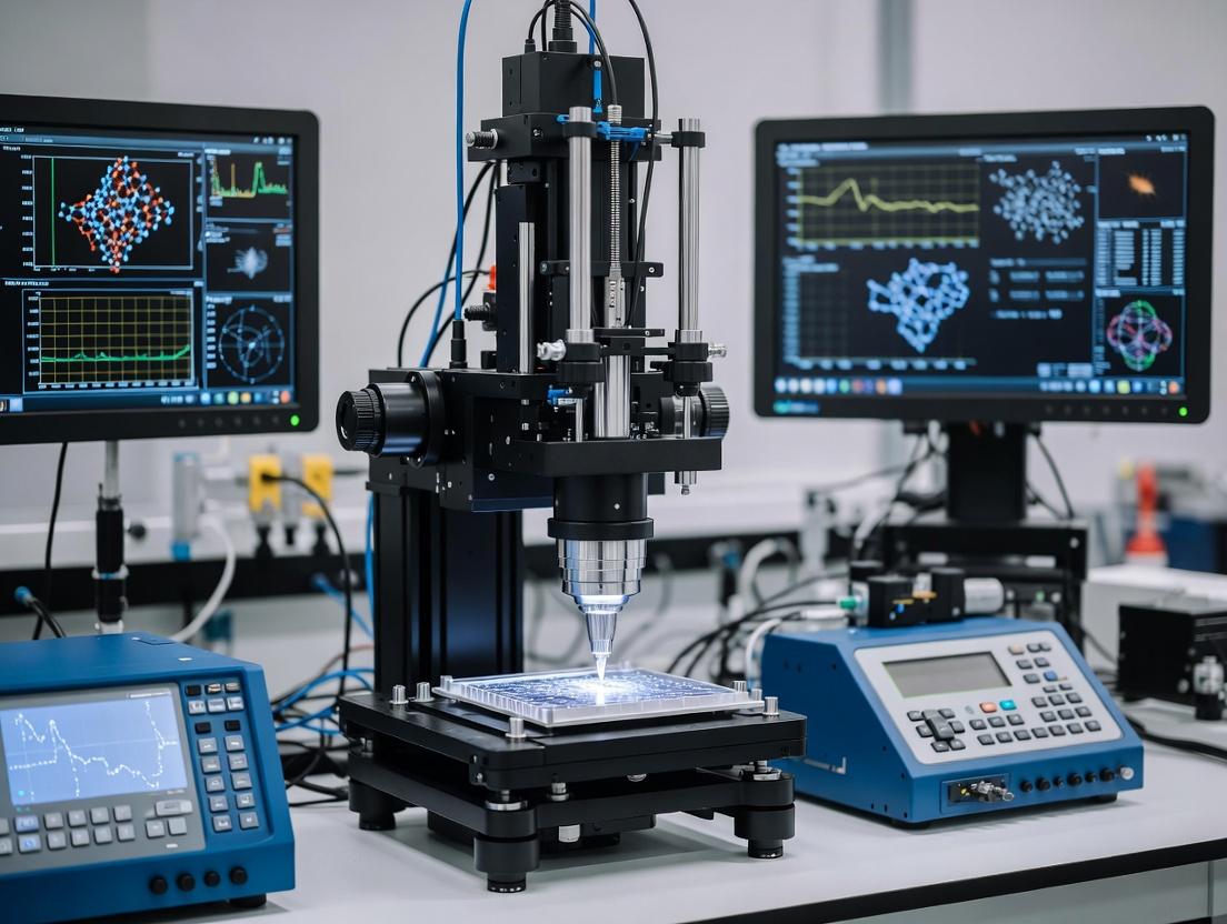
Beyond Topography: How KPFM-Enhanced AFM Maps Chemical Composition for Advanced Biomedical Research
This comprehensive article details the integration of Atomic Force Microscopy (AFM) with Kelvin Probe Force Microscopy (KPFM) for nanoscale chemical composition mapping.
Beyond Topography: How KPFM-Enhanced AFM Maps Chemical Composition for Advanced Biomedical Research
Abstract
This comprehensive article details the integration of Atomic Force Microscopy (AFM) with Kelvin Probe Force Microscopy (KPFM) for nanoscale chemical composition mapping. Aimed at researchers and drug development professionals, it explores the foundational principles of KPFM for quantifying surface potential and work function, translating into material identification. The core focus is on practical methodologies and applications, particularly in characterizing drug delivery systems, biomaterials, and protein interactions. We provide actionable troubleshooting and optimization strategies to overcome common challenges like environmental noise and tip degradation. Finally, the article validates KPFM's capabilities by comparing it with complementary techniques like XPS and Raman spectroscopy, establishing its unique role in correlating nanomechanical, electrical, and chemical properties for transformative insights in biomedical research.
The Science Behind the Signal: Decoding Surface Potential for Chemical Identification with KPFM
Atomic Force Microscopy (AFM) is a cornerstone technique in nanoscale characterization, providing topographical mapping with angstrom-level resolution. Within the broader thesis on AFM for chemical composition mapping, Kelvin Probe Force Microscopy (KPFM) emerges as a critical derivative. It bridges pure mechanical surface sensing with local electrical property measurement. This application note details protocols for correlative AFM/KPFM analysis, targeting researchers in materials science, semiconductor development, and drug discovery where surface potential mapping can reveal chemical heterogeneity, charge distribution, and work function variations crucial for understanding molecular interactions and device performance.
Quantitative Comparison of AFM Operational Modes
The choice of AFM mode directly impacts the feasibility and resolution of subsequent KPFM measurements.
Table 1: Comparison of Primary AFM Modes for KPFM Integration
| AFM Mode | Principle | Topography Resolution | KPFM Compatibility | Best For Samples |
|---|---|---|---|---|
| Contact Mode | Direct tip-surface contact. | High (<1 nm) | Poor. High friction/forces interfere with electrical signals. | Hard, stable surfaces where electrical data is not priority. |
| Tapping Mode (AC) | Tip oscillates at resonance, intermittently touching surface. | High (<1 nm) | Good. Reduces lateral forces. Standard for ambient KPFM. | Most ambient samples (polymers, biological, thin films). |
| PeakForce Tapping | Precisely controls maximum force on each tap. | Very High (<0.5 nm) | Excellent. Optimal force control preserves tip and sample integrity. | Soft, delicate samples (live cells, organic photovoltaics). |
| Frequency Modulation (FM) - UHV | Oscillates at constant amplitude, frequency shift is feedback. | Atomic | Excellent. Standard for high-resolution KPFM in UHV. | Atomic-scale studies on conductors/semiconductors in UHV. |
Core KPFM Measurement Principles and Protocols
KPFM measures the Contact Potential Difference (CPD) between a conductive AFM tip and the sample. CPD = (Φsample - Φtip) / (-e), where Φ is work function.
Primary KPFM Detection Modes
Table 2: KPFM Operational Modes
| Mode | Detection Method | Spatial Resolution | Sensitivity | Protocol Summary |
|---|---|---|---|---|
| AM-KPFM (Lift Mode) | Amplitude detection of electrostatic force at ω_AC. | Lower (~50-100 nm). Dual-pass limits resolution. | Good for ambient conditions. | Two-pass method: 1st pass: Topography in tapping mode. 2nd lift pass: Tip retraces height + lift offset (~20-100 nm), applies VAC; VDC nullifies amplitude. |
| FM-KPFM (Single-Pass) | Frequency shift detection of electrostatic force gradient at ω_AC. | Higher (~10-20 nm). Single-pass enables better correlation. | Superior in UHV/Vacuum. | Single-pass method: Topography feedback from mechanical oscillation (e.g., frequency shift). Simultaneously, VAC applied; VDC nullifies frequency shift sideband. |
Detailed Experimental Protocol: Correlative Topography and Surface Potential Mapping
Protocol Title: Single-Pass PeakForce-KPFM on a Hybrid Organic-Inorganic Perovskite Film
Objective: To simultaneously acquire nanoscale topography and local surface potential (work function) maps, identifying phase segregation or charge trapping sites.
I. Sample Preparation
- Substrate: Use ITO-coated glass slides. Clean via sequential ultrasonication in Hellmanex III solution, deionized water, and isopropanol (15 min each). Dry with N₂.
- Sample Deposition: Spin-coat your perovskite precursor solution (e.g., MAPbI₃) in a nitrogen-filled glovebox (O₂, H₂O <1 ppm). Anneal on hotplate per established literature (e.g., 100°C for 10 min).
- Mounting: Secure the sample to a 12 mm AFM metal puck using a double-sided carbon tab to ensure electrical grounding.
II. AFM/KPFM Setup
- System: Use a commercial AFM (e.g., Bruker Dimension Icon, Cypher S) equipped with a PeakForce KPFM module and an environmental control chamber.
- Probe Selection: Use a conductive, Pt/Ir-coated silicon probe (e.g., Bruker SCM-PIT-V2). Nominal resonance frequency: ~75 kHz, spring constant: ~2.8 N/m. Critical: Confirm coating integrity via SEM if possible.
- Environmental Control: Perform measurement in a dry nitrogen atmosphere (<5% RH) to minimize water layer effects on CPD.
III. Measurement Procedure
- Engagement: Engage the tip in standard PeakForce Tapping mode to obtain stable, low-force (<100 pN) topography.
- KPFM Parameter Optimization:
- Set the AC bias frequency (
ω_AC) to a value between 10-50 kHz lower than the mechanical resonance to avoid crosstalk. - Set AC bias amplitude (
V_AC) typically between 1-3 V. - Enable single-pass PeakForce-KPFM mode. The system will now superimpose the electrostatic excitation on each mechanical "tap."
- Set the AC bias frequency (
- Feedback Loop Tuning:
- Topography Channel: Adjust PeakForce Setpoint and feedback gains to achieve stable tracking.
- KPFM Channel (CPD): Tune the proportional-integral (PI) feedback gains for the DC bias (
V_DC) loop. Start with low gains, increase until the CPD signal is stable without oscillation.
- Data Acquisition: Scan an area of interest (e.g., 5 µm x 5 µm) at a resolution of 512 x 512 pixels. Scan rate: 0.3-0.5 Hz.
IV. Data Analysis & Calibration
- Topography Analysis: Analyze root-mean-square (RMS) roughness, grain size distribution.
- CPD to Work Function Conversion: The measured CPD is relative. To get absolute sample work function (
Φ_sample):Φ_sample = Φ_tip - e * CPD- Calibrate
Φ_tipusing a reference sample of known, stable work function (e.g., freshly cleaved HOPG, Φ ≈ 4.48 eV, or Au foil, Φ ≈ 5.1 eV). Measure CPD on the reference under identical conditions.
Visualizing the Workflow and Signal Pathways
Diagram Title: AFM/KPFM Experimental Workflow and Signal Nullification
The Scientist's Toolkit: Essential Research Reagents & Materials
Table 3: Key Research Reagent Solutions for AFM/KPFM Studies
| Item/Reagent | Function & Importance | Example Product/Chemical |
|---|---|---|
| Conductive AFM Probes | Coated with Pt/Ir, Au, or doped diamond to enable electrical sensing. Coating durability is critical. | Bruker SCM-PIT (Pt/Ir), NanoWorld ARROW-EFM (Au), AD-2.8-AS (diamond). |
| Reference Work Function Samples | Essential for calibrating the tip work function (Φ_tip) to convert CPD to absolute values. |
Freshly cleaved HOPG (Φ~4.48 eV), Evaporated Au on Mica (Φ~5.1 eV). |
| Conductive Substrates | Provide electrical grounding for the sample, preventing charge accumulation during KPFM. | ITO-coated glass, Highly Ordered Pyrolytic Graphite (HOPG), Silicon with ~300 nm thermal oxide (for grounding via substrate coating). |
| Cleaning Solutions | Ensure sample and substrate are free of organic contaminants that affect topography and CPD. | Hellmanex III, Micro-90, or Piranha solution (H₂SO₄:H₂O₂) for substrates. Caution: Use appropriate safety protocols. |
| Environmental Control Media | Inert gas or dry air to suppress surface water layer, a major source of CPD measurement artifacts. | Ultra-high purity nitrogen (N₂) gas, dry air generator systems. |
| Vibration Isolation System | Critical for achieving high-resolution imaging by isolating the AFM from ambient building vibrations. | Active vibration cancellation platforms (e.g., Herzan, Accurion), pneumatic isolation tables. |
Contact Potential Difference (CPD) is the voltage that arises between two materials when they are brought into electrical contact. It is a direct consequence of the difference in their work functions (Φ). The work function is the minimum energy (usually expressed in electronvolts, eV) required to remove an electron from the Fermi level of a material to a point in the vacuum just outside the material surface. When two materials with different work functions (Φ1 and Φ2, where Φ1 > Φ2) are connected electrically, electrons flow from the material with the lower work function to the one with the higher work function until their Fermi levels equilibrate. This electron transfer creates an electric field and a potential difference across the gap between the two materials, which is the CPD.
The fundamental relationship is: CPD = (Φtip - Φsample) / (-e) where e is the elementary charge. In Kelvin Probe Force Microscopy (KPFM), this principle is used to measure the local work function or surface potential of a sample with nanometer resolution, which is critical for chemical composition mapping.
Table 1: Typical Work Function Values of Common Materials
| Material | Work Function (eV) | Notes / Application in KPFM |
|---|---|---|
| Gold (Au) | ~5.1 - 5.5 | Common conductive coating for AFM tips; reference material. |
| Platinum/Iridium (Pt/Ir) | ~5.3 - 5.7 | Used for conductive AFM tips due to hardness and stability. |
| Highly Oriented Pyrolytic Graphite (HOPG) | ~4.6 | Often used as an atomically flat calibration sample. |
| Silicon (n-doped) | ~4.0 - 4.3 | Common substrate; work function depends on doping level. |
| Silicon (p-doped) | ~4.9 - 5.2 | Common substrate; work function depends on doping level. |
| Indium Tin Oxide (ITO) | ~4.4 - 4.8 | Transparent conductive oxide used in organic electronics. |
| Polythiophene (P3HT) | ~4.8 - 5.0 | Example organic semiconductor; varies with processing. |
Table 2: Key Performance Parameters in KPFM Measurement
| Parameter | Typical Range / Value | Impact on CPD Measurement |
|---|---|---|
| Spatial Resolution | 10 - 50 nm (ambient), < 10 nm (UHV) | Determines feature detection limit in composition maps. |
| Voltage Sensitivity | < 1 mV | Critical for detecting subtle work function variations. |
| Tip-Sample Distance (Lift Height) | 10 - 100 nm | Balances capacitive force signal and spatial resolution. |
| AC Modulation Voltage (V_ac) | 1 - 10 V | Drives the electrostatic force; optimal amplitude is sample-dependent. |
| Frequency (ω) | ~10 - 100 kHz | Applied near the resonant frequency of the cantilever for sensitivity. |
Experimental Protocols for KPFM-Based CPD Measurement
Protocol 1: Calibration of the KPFM System Using Reference Samples
Objective: To calibrate the absolute work function measurement of the AFM tip using a sample of known work function. Materials: Conductive AFM tip (Pt/Ir coating), Au-coated substrate (known Φ), HOPG substrate. Procedure:
- Engage in Tapping Mode: Engage the tip on the Au surface in standard AFM tapping mode to obtain topography.
- Switch to KPFM Mode: Activate the dual-pass (lift mode) KPFM operation. a. First Pass: Trace topography in standard tapping mode. b. Second Pass: Retrace the profile at a user-defined lift height (e.g., 50 nm) with tapping disabled.
- Apply AC Bias: Apply a sinusoidal voltage (V_ac, e.g., 2-5 V, ω) to the tip.
- Nullify Force: Use a feedback loop (typically using a lock-in amplifier) to apply a DC bias (Vdc) to the tip until the electrostatic force at frequency ω is nulled. This Vdc is the negative CPD.
- Record Vdc on Au: The measured CPD is: CPDAu = V_dc.
- Calculate Tip Work Function: Φtip = ΦAu + e * CPD_Au.
- Validate: Repeat measurement on a second reference (e.g., HOPG) to confirm consistency.
Protocol 2: Mapping Chemical Composition via Work Function on a Pharmaceutical Blend
Objective: To map component distribution in a drug-polymer blend based on local work function differences. Materials: Model system (e.g., API like Ibuprofen crystals embedded in a PVP polymer matrix), conductive tip. Procedure:
- Sample Preparation: Spin-coat or press a smooth, thin film of the blend onto a conductive substrate (e.g., ITO or Si wafer).
- Topography Imaging: Perform a tapping mode scan to obtain surface morphology.
- Simultaneous KPFM Scan: Enable single-pass or dual-pass KPFM to acquire the surface potential map simultaneously with or immediately after topography.
- Data Acquisition: The feedback loop continuously adjusts Vdc to nullify the electrostatic force at each pixel. This Vdc(x,y) map represents the local CPD.
- Conversion to Work Function: Using the calibrated Φtip from Protocol 1, calculate the local sample work function at each pixel: Φsample(x,y) = Φ_tip - e * CPD(x,y).
- Correlation and Analysis: Overlay the Φ_sample map with topography. Different chemical phases (API vs. polymer) will exhibit distinct work function values, allowing for phase identification and distribution analysis.
Mandatory Visualizations
Title: Electron Flow and CPD Formation Between Two Materials
Title: KPFM Workflow for Chemical Composition Mapping
The Scientist's Toolkit: Key Research Reagent Solutions
Table 3: Essential Materials for KPFM Experiments
| Item | Function & Importance | Example/Notes |
|---|---|---|
| Conductive AFM Probes | Serve as the mobile electrode for CPD measurement. Coating determines tip work function (Φ_tip). | Pt/Ir-coated Si tips, Diamond-coated tips, Cr/Pt-coated Si tips. |
| Reference Calibration Samples | Provide known, stable work function surfaces to calibrate Φ_tip absolutely. | Freshly evaporated Au films, HOPG, Ag, or doped Si wafers. |
| Conductive Substrates | Provide electrical back-contact for samples, especially non-conductive ones, and prevent charging. | ITO-coated glass, Si wafers (heavily doped), Au-coated mica. |
| Lock-in Amplifier | Extracts the tiny electrostatic force signal at the modulation frequency (ω) with high signal-to-noise. | Integral part of modern AFM/KPFM controllers. |
| Environmental Control Chamber | Minimizes surface water layers and contaminants which drastically affect work function measurements. | Glove box, vacuum chamber, or environmental AFM stage. |
| Vibration Isolation System | Essential for high-resolution imaging by isolating the AFM from building and acoustic noise. | Active or passive air table systems. |
| Software for Data Analysis | For processing CPD maps, correlating with topography, and statistical analysis of phase distribution. | Gwyddion, Nanoscope Analysis, MATLAB/Python with custom scripts. |
How Surface Potential Maps Reveal Chemical Heterogeneity and Material Phases
Atomic Force Microscopy (AFM), particularly Kelvin Probe Force Microscopy (KPFM), has emerged as a cornerstone technique for nanoscale chemical composition mapping. The broader thesis of modern KPFM research posits that surface potential (SP or CPD - Contact Potential Difference) is a direct reporter of local work function variations, which are intrinsically linked to chemical identity, molecular orientation, doping levels, and charge states. This application note details how SP maps, acquired via KPFM, decode chemical heterogeneity and distinguish material phases that are otherwise indistinguishable by topography alone, with direct relevance to materials science and pharmaceutical development (e.g., polymorphism, blend morphology, contamination).
Foundational Principles: From Surface Potential to Chemistry
The measured contact potential difference (VCPD) in KPFM is given by: VCPD = (Ψsample - Ψtip) / (-e), where Ψ is the work function and e is the elementary charge. Variations in V_CPD across a surface directly correlate with changes in the sample's local work function. Key factors influencing work function include:
- Chemical Composition: Different elements or molecules have distinct ionization energies and electron affinities.
- Crystalline Phase & Orientation: Different atomic arrangements alter surface dipole layers.
- Doping Concentration (Semiconductors): Changes in Fermi level position.
- Adsorbates & Contamination: Local changes in surface dipole moments.
- Charge Trapping: In dielectrics or organic semiconductors, trapped charges create localized potential shifts.
Application Notes: Decoding Heterogeneity in Key Systems
Pharmaceutical Polymorph Characterization
Active Pharmaceutical Ingredients (APIs) can exist in multiple polymorphic forms with distinct physicochemical properties (e.g., solubility, bioavailability). KPFM distinguishes polymorphs based on surface potential differences arising from molecular packing and surface dipole orientation.
Key Quantitative Data: Table 1: Surface Potential of Common API Polymorphs (Representative Data from Literature)
| API (e.g., Carbamazepine) | Polymorph Form | Avg. Surface Potential (mV) | Std. Dev. (mV) | Relative Work Function Shift |
|---|---|---|---|---|
| Carbamazepine | Form III | -25 | 5 | Reference |
| Carbamazepine | Form I | +180 | 8 | ~205 mV Higher |
| Sulfathiazole | Form I | -50 | 10 | Reference |
| Sulfathiazole | Form II | +120 | 15 | ~170 mV Higher |
Experimental Protocol for API Polymorph Mapping:
- Sample Preparation: Prepare a co-crystallized or compacted sample containing a mixture of polymorphs (e.g., via drop-casting from a slurry of different forms onto a conductive substrate like HOPG or Au). Ensure a flat, dry surface.
- AFM/KPFM Setup: Use a shielded environmental chamber to minimize humidity and electrostatic noise. Employ a conductive, Pt/Ir-coated AFM tip.
- Topography Scan: First, acquire a high-resolution topography map in tapping mode to identify gross morphological features (e.g., crystal facets).
- KPFM Measurement: Engage the KPFM module. Typically, use a two-pass technique (Lift Mode): First pass records topography; second pass retraces the profile at a constant lift height (e.g., 20-50 nm) while applying an AC voltage and a DC nulling voltage to the tip to measure V_CPD.
- Parameters: AC voltage: 1-3 V, frequency: ~70 kHz (off-resonance), lift height: 20-50 nm, scan rate: 0.3-0.5 Hz.
- Data Correlation: Overlay the SP map onto the topography. Distinct regions with uniform potential, despite similar topography, are assigned to specific polymorphs via calibration against pure form standards.
Organic Photovoltaic (OPV) Blend Morphology
In bulk heterojunction OPVs, the nanoscale phase separation between donor (P3HT, PBDB-T) and acceptor (PCBM, ITIC) materials critically impacts device efficiency. KPFM maps potential differences due to the distinct work functions of the components.
Key Quantitative Data: Table 2: Surface Potential of Common OPV Materials
| Material | Type | Avg. Work Function (eV) | Avg. KPFM V_CPD (vs. Au tip, mV) | Notes |
|---|---|---|---|---|
| P3HT | Donor | 4.9 - 5.1 | +150 to +300 | Depends on regioregularity |
| PBDB-T | Donor | ~4.8 | +50 to +200 | |
| PCBM | Acceptor | 6.0 - 6.2 | -300 to -500 | |
| ITIC | Acceptor | ~5.9 | -250 to -450 | |
| Au Substrate | Electrode | 5.1 | 0 (Reference) | Tip work function referenced |
Experimental Protocol for OPV Blend Phase Mapping:
- Sample Preparation: Spin-coat the OPV active layer blend (e.g., P3HT:PCBM in chlorobenzene) onto an ITO or Au substrate. Anneal as required to induce phase separation.
- AFM/KPFM Setup: Use a conductive diamond-coated tip for durability against the often rough film surfaces. Perform measurements in a nitrogen glovebox or inert atmosphere to prevent oxidation.
- Simultaneous Measurement: Use a single-pass, frequency-modulation KPFM (FM-KPFM) technique if available, as it offers higher spatial resolution by measuring at the first resonance. Otherwise, use standard two-pass lift mode.
- Parameters (Lift Mode): Lift height: 10-30 nm (critical for resolution), AC Voltage: 2 V, Scan rate: 0.4 Hz.
- Phase Analysis: The SP map will show interconnected domains. The higher potential (more positive) domains correspond to the donor material, while the lower potential (more negative) domains correspond to the acceptor. Histogram analysis of the SP map quantifies the domain purity and intermixing.
The Scientist's Toolkit: Key Research Reagent Solutions
Table 3: Essential Materials for KPFM-based Chemical Mapping
| Item | Function & Explanation |
|---|---|
| Conductive AFM Probes (Pt/Ir or Au-Coated) | Coating provides a conductive path for the KPFM bias voltage and a well-defined tip work function. Pt/Ir offers durability. |
| Diamond-Coated AFM Probes | Essential for scanning rough or hard samples (e.g., annealed polymer films, some crystals) without wearing through the conductive coating. |
| Highly Ordered Pyrolytic Graphite (HOPG) | An atomically flat, conductive substrate crucial for calibrating KPFM measurements and preparing flat-lying samples (e.g., nanoparticles, molecules). |
| Gold or ITO-Coated Substrates | Standard conductive substrates for spin-coating films. Au provides a chemically inert, low-roughness surface with a known work function. |
| Environmental Control Chamber | A sealed chamber with ports for gas purging (N2, Ar) to control humidity and oxygen, preventing surface oxidation and water layer formation that swamp SP signals. |
| Vibration Isolation System | An active or passive isolation table is mandatory, as KPFM is highly sensitive to vibrational noise which degrades the sensitive nulling feedback loop. |
| Calibration Gratings (e.g., KPFM Sample) | Pre-patterned samples with known potential differences (e.g., metal electrodes on SiO2) to verify the accuracy and resolution of the KPFM system. |
Experimental & Data Analysis Workflows
Diagram Title: General KPFM Workflow for Chemical Phase Mapping
Diagram Title: Surface Potential Data Analysis Pathway
This document details the advanced instrumentation and methodology central to achieving high-resolution chemical composition mapping via Kelvin Probe Force Microscopy (KPFM) within Atomic Force Microscopy (AFM). The broader thesis posits that the precise integration of these key components is critical for surpassing the limitations of conventional KPFM, enabling nanoscale mapping of work functions and surface potentials with minimal crosstalk for applications in materials science and pharmaceutical development.
Core Components: Technical Specifications & Function
The Dual-Pass (Lift-Mode) Technique
A two-pass scan methodology designed to decouple topographic from electrical/chemical information.
- First Pass: Engages standard TappingMode to acquire high-resolution topography.
- Second Pass (Lift Mode): The probe retraces the stored topography at a constant lift height (typically 10-100 nm), with only long-range electrical forces active. This separation drastically reduces topographic crosstalk.
Conductive Probes
Specialized AFM probes with a conductive coating (e.g., Pt/Ir, Au/Cr, or doped diamond) and a sharp apex (< 30 nm radius). They serve as a movable electrical electrode for applying AC and DC biases and detecting the resultant electrostatic force.
Lock-In Detection
A phase-sensitive demodulation technique. An AC voltage (Vac sin(ωt)) is applied to the probe. The resulting electrostatic force at ω (for KPFM) is isolated by the lock-in amplifier. The output is used in a feedback loop to nullify the force by applying a compensating DC voltage (Vdc), which equals the Contact Potential Difference (CPD).
Application Notes
Primary Application: Nanoscale chemical composition mapping via local work function differences. In drug development, this enables the study of API (Active Pharmaceutical Ingredient) distribution in solid dispersions, polymorphism identification, and surface potential mapping of lipid bilayers or protein aggregates.
Advantages over Single-Pass KPFM:
- Reduced Topographic Artefact: The lift mode eliminates the primary source of error in CPD measurement.
- Preserved Probe Integrity: Reduced wear on the conductive coating.
- Compatibility: Allows simultaneous collection of other lift-mode signals (e.g., magnetic, capacitive).
Key Limitation: Reduced spatial resolution in the potential map compared to the topographic image, as the lift height broadens the probe-sample electrostatic interaction.
Quantitative Performance Data:
Table 1: Typical Operational Parameters and Performance Metrics for Dual-Pass KPFM
| Parameter | Typical Range | Impact on Measurement |
|---|---|---|
| Lift Height | 10 - 100 nm | Higher lift reduces crosstalk but degrades spatial resolution. |
| AC Bias (V_ac) | 1 - 5 V | Larger amplitude improves SNR but may induce sample charging. |
| AC Frequency (ω) | 10 - 100% of cantilever resonance | Must be distinct from mechanical drive frequency to avoid interference. |
| CPD Resolution | < 5 mV | Achievable with optimized lock-in time constants and low-noise probes. |
| Spatial Resolution | 20 - 50 nm (Potential Map) | Dictated by probe radius and lift height, not topographic resolution. |
| Scan Rate (Lift Pass) | 0.3 - 0.8 Hz | Slower than first pass to ensure accurate tracking and signal stability. |
Detailed Experimental Protocol: Dual-Pass KPFM for API Distribution Mapping
Objective: To map the surface potential/CPD of a solid dispersion tablet blend to identify domains of a hydrophobic API within a hydrophilic polymer matrix.
Materials & Reagents (The Scientist's Toolkit)
Table 2: Essential Research Reagent Solutions & Materials
| Item | Function / Description |
|---|---|
| Conductive AFM Probe | Pt/Ir-coated Si cantilever (k ~ 2-5 N/m, f0 ~ 70 kHz). Provides electrical contact and mechanical sensing. |
| Sample: Microtomed Tablet Surface | A smooth, ~100 nm thick cross-section of the solid dispersion, prepared by ultramicrotomy and mounted on a conductive substrate (e.g., Si wafer with Au coating). |
| Conductive Substrate (Au-coated Si) | Provides a grounded, flat backing for sample mounting and a reference electrical plane. |
| Vibration Isolation Enclosure | Acoustic hood or active isolation table. Minimizes vibrational noise for stable lift-mode operation. |
| Desiccator | For sample storage to prevent adsorption of atmospheric water, which alters local CPD. |
Procedure
System Setup & Calibration:
- Mount the sample on the conductive substrate using a thin layer of conductive carbon tape.
- Insert the conductive probe and align the laser on the cantilever.
- Perform thermal tuning to determine the cantilever's resonance frequency and quality factor in air.
- Engage TappingMode on a clean, featureless area of the sample (e.g., pure polymer region) to optimize feedback gains.
Topography Acquisition (First Pass):
- Select the scan area (e.g., 5 µm x 5 µm).
- Engage the standard TappingMode. Set scan rate to 0.5-1.0 Hz.
- Acquire and save the high-resolution topographic image. Ensure the trace and retrace are consistent.
Dual-Pass KPFM Setup (Second Pass):
- Enable the dual-pass/lift-mode function in the AFM software.
- Set the lift height (e.g., 30 nm).
- Configure the electrical module:
- Apply an AC bias (Vac = 2 V, ω = ωdrive + 1 kHz) to the probe.
- Route the cantilever deflection signal to a lock-in amplifier referenced to ω.
- Set the lock-in amplifier's time constant to 1-10 ms (balances noise vs. responsiveness).
- Enable the KPFM feedback loop, which will output Vdc.
CPD Map Acquisition (Lift Pass):
- Initiate the second pass. The system will retrace the stored topography at the set lift height.
- The lock-in detects the electrostatic force at ω. The feedback loop adjusts Vdc to null this force.
- The recorded Vdc map is the CPD map. Simultaneously, the amplitude of the electrostatic force (error signal) can be recorded.
Data Correlation & Analysis:
- Co-register the topographic and CPD maps.
- Regions of differing chemical composition (e.g., API vs. polymer) will show distinct CPD values (contrast).
- Use histogram analysis of the CPD map to statistically differentiate phases.
Visualization: Workflow & System Logic
Diagram 1: Dual-Pass KPFM Experimental Workflow
Diagram 2: KPFM Lock-In Detection and Feedback System
The Fundamental Link Between Local Work Function and Surface Chemistry
Within the context of mapping chemical composition via Kelvin Probe Force Microscopy (KPFM), the local work function (WF) is the fundamental descriptor linking surface electronic structure to chemical identity. Variations in surface chemistry—adsorbates, molecular dipoles, oxidation states, or heterogeneous domains—directly modulate the WF. This application note details how KPFM exploits this link for nanoscale chemical mapping, providing protocols for correlative analysis critical for materials science and pharmaceutical surface characterization.
Theoretical Framework: Work Function Determinants
The work function (Φ) is the minimum energy required to remove an electron from the Fermi level of a solid to vacuum. It is governed by the equation: Φ = -eϕ + μ where eϕ is the surface dipole contribution and μ is the bulk chemical potential. Surface chemistry alters ϕ via:
- Adsorbate Dipoles: Electron-donating/withdrawing species create opposing surface dipoles.
- Molecular Orientation: Ordered monolayers with permanent dipoles (e.g., self-assembled monolayers) shift WF.
- Oxidation State & Composition: Different terminations or stoichiometries (e.g., metal vs. oxide) change the surface dipole layer.
Table 1: Work Function Shifts for Common Surface Chemical Modifications
| Surface Modification | System Example | Typical WF Shift (eV) | Primary Mechanism |
|---|---|---|---|
| Alkali Metal Adsorption | Cs on Au(111) | -2.0 to -3.5 | Strong positive-outward dipole from charge transfer |
| Oxygen Adsorption/ Oxidation | O₂ on Cu(110) | +0.3 to +1.5 | Negative-outward dipole; electron withdrawal |
| Self-Assembled Monolayer (Thiol) | CH₃-terminated on Au | -0.9 to -1.2 | Dipole layer from S-Au bond + terminal group |
| Self-Assembled Monolayer (Thiol) | CF₃-terminated on Au | +0.9 to +1.2 | Strong electronegativity of terminal group |
| Graphene Doping | Graphene on SiO₂ vs. h-BN | ±0.2 to 0.5 | Charge transfer from substrate, doping level |
KPFM Protocols for Chemical Mapping
Protocol 1: Two-Pass Amplitude-Modulation KPFM (AM-KPFM)
Objective: Map surface potential (CPD) with high spatial resolution to infer chemical heterogeneity. Workflow: See Diagram 1. Key Reagents & Materials: See Table 2.
Procedure:
- Probe Preparation: Use conductive, Pt/Ir-coated or doped diamond-coated AFM probes (force constant ~2-5 N/m, resonance frequency ~75 kHz). Clean in UV-ozone for 15 minutes.
- Sample Preparation: For drug formulations, prepare by microtoming or spin-coating on a conductive substrate (e.g., HOPG, ITO). Ensure electrical connectivity.
- Topography Scan: First pass: Operate in tapping mode to acquire high-resolution topography. Set parameters to minimize tip wear (amplitude setpoint ~80% of free amplitude).
- CPD Scan: Second pass: Lift height = 10-20 nm. The tip is electrically biased with AC voltage (Vac, amplitude 1-3 V, frequency ω) and DC offset (Vdc). The electrostatic force at ω is nullified by a feedback loop that adjusts Vdc to equal the CPD. This Vdc is recorded as the CPD map.
- Calibration: Verify using a known potential standard (e.g., graphite steps, HOPG).
Protocol 2: Single-Pass Frequency-Modulation KPFM (FM-KPFM)
Objective: Achieve higher spatial resolution CPD mapping, suitable for atomic-scale chemical variations. Procedure:
- Probe & Setup: Use a high-resolution qPlus sensor (stiff cantilever, ~1800 N/m) with a metallic tip. System must allow simultaneous detection of frequency shift.
- Synchronized Detection: Apply Vac + Vdc bias at the tip. The electrostatic force gradient shifts the cantilever resonance frequency. A lock-in amplifier detects the component at ω.
- Feedback Loop: The ω signal is fed to a nullifying feedback controller that continuously adjusts V_dc to match the instantaneous local CPD as the tip scans.
- Data Acquisition: Topography and CPD are acquired simultaneously in a single pass, eliminating lift-mode artifacts.
Table 2: Research Reagent Solutions & Essential Materials
| Item | Function in KPFM Chemical Mapping |
|---|---|
| Conductive Probes (Pt/Ir Coated) | Provides electrical contact for bias application; coating defines tip work function reference. |
| Doped Diamond-Coated Probes | Offers extreme wear resistance for scanning abrasive samples (e.g., ceramics, oxides). |
| Highly Ordered Pyrolytic Graphite (HOPG) | Atomically flat, conductive calibration standard for both topography and potential. |
| ITO-Coated Glass Slides | Transparent, conductive substrate for thin-film or organic sample support. |
| Gold-coated Substrate | Standard for SAM formation; provides uniform, chemically tunable surface. |
| UV-Ozone Cleaner | Removes organic contaminants from probes and substrates pre-experiment. |
| Self-Assembled Monolayer (SAM) Kits | Model systems (e.g., alkanethiols with -CH₃, -COOH, -NH₂ termini) for controlled WF shift calibration. |
| Vibration Isolation Enclosure | Critical for reducing acoustic/mechanical noise to achieve mV-level CPD resolution. |
| Environmental Control Chamber | Allows experiments in inert gas or controlled humidity to prevent surface oxidation/contamination. |
Diagram 1: AM-KPFM Two-Pass Chemical Mapping Workflow.
Diagram 2: The Core Link from Chemistry to KPFM Signal.
Data Interpretation & Correlation
The measured CPD is: VCPD = (Φtip - Φsample) / e. A lower sample WF relative to the tip yields a more positive VCPD.
- Chemical Identification: Correlate known WF values (Table 1) with measured CPD domains.
- Quantitative Analysis: Profile line scans across domain boundaries to measure interfacial width of chemical change.
- Artifact Avoidance: Ensure topography-CPD correlation is real, not from capacitive coupling or tip artifacts (verify with reverse bias).
KPFM transforms the fundamental link between local work function and surface chemistry into a quantitative nanoscale mapping tool. For drug development, this enables the characterization of API distribution in solid dispersions, coating heterogeneity, and surface potential of lipid nanoparticles, directly informing stability and performance. Precise protocols and controlled model systems are essential for accurate chemical interpretation.
Protocols in Practice: Step-by-Step KPFM for Biomedical Sample Analysis
Optimal Sample Preparation for Drug Formulations, Lipid Bilayers, and Biological Tissues
This application note details standardized sample preparation protocols critical for obtaining reliable and reproducible nanoscale chemical composition maps using Atomic Force Microscopy (AFM) modes like Kelvin Probe Force Microscopy (KPFM) and related techniques. Accurate KPFM measurements of surface potential are exceptionally sensitive to sample preparation artifacts, making the following procedures foundational to a broader thesis on correlating nanoscale structure with chemical and electronic properties in biophysical systems.
Application Notes & Protocols
1. Drug Formulation Nanoparticles (Polymeric/Lipidic) Objective: To prepare uniform, isolated nanoparticles for KPFM analysis of API (Active Pharmaceutical Ingredient) distribution and shell-core potential differences. Challenge: Aggregation prevents single-particle analysis; excessive surface roughness convolutes electronic potential measurements.
| Step | Parameter | Optimal Range / Specification | Rationale for KPFM |
|---|---|---|---|
| Purification | Method | Dialysis or Size-Exclusion Chromatography | Removes free ions & polymers that create fluctuating surface potentials. |
| Dilution | Solvent | Particle-free deionized water or original buffer | Maintains colloidal stability without introducing contaminants. |
| Substrate | Choice | Freshly cleaved Mica or HOPG (Highly Ordered Pyrolytic Graphite) | Provides an atomically flat, conductive (HOPG) or semi-conductive (mica) reference surface. |
| Deposition | Concentration | 1-5 µg/mL | Ensures isolated particles for single-point spectroscopy. |
| Deposition | Time | 5-10 minutes (incubation) | Prevents multilayer formation. |
| Drying | Method | Ambient air drying in laminar flow hood OR gentle N₂ stream | Controlled drying minimizes coffee-ring effects that alter local conductivity. |
| Final State | Hydration | For KPFM: Typically dry measurement | Eliminates water meniscus, a major source of potential noise. |
Detailed Protocol:
- Purify nanoparticle suspension via dialysis against DI water for 24h (with 3-4 water changes) to remove salts and unencapsulated API.
- Dilute the purified stock to a final concentration of ~2 µg/mL in particle-free water.
- Cleave a mica sheet (approx. 1x1 cm) using adhesive tape to expose a fresh, atomically flat surface.
- Deposit 20 µL of the diluted suspension onto the mica surface. Incubate for 7 minutes in a covered Petri dish to prevent dust contamination.
- Gently rinse the surface with 2 mL of particle-free DI water applied at a ~45° angle to remove loosely adhered particles.
- Dry the sample under a gentle, ultrapure nitrogen stream for 2 minutes.
- Mount the sample on the AFM metal puck using a conductive double-sided carbon tape to ensure electrical grounding for KPFM.
2. Supported Lipid Bilayers (SLBs) Objective: To form defect-free, fluidic bilayers on a flat substrate for mapping domain-specific surface potentials. Challenge: Achieving complete bilayer coverage without vesicles or defects that cause topographic and potential artifacts.
| Step | Parameter | Optimal Range / Specification | Rationale for KPFM |
|---|---|---|---|
| Lipid Choice | Composition | DOPC with 10-30% cholesterol & labeled lipid (e.g., DPPC, GM1) | Creates phase-separated domains with distinct work functions. |
| Vesicle Prep | Extrusion | Through 50 nm pore polycarbonate membrane, 21 times | Creates small unilamellar vesicles (SUVs) for even fusion. |
| Substrate | Choice | Silica-coated glass disc or freshly cleaved mica | High surface charge promotes vesicle rupture and bilayer formation. |
| Cleaning | Method | Oxygen plasma treatment for 15 minutes | Creates hydrophilic, ultra-clean surface for uniform fusion. |
| Deposition | Temperature | Above lipid main phase transition (e.g., 37°C for DOPC) | Ensures fluidity for vesicle rupture and domain formation. |
| Rinsing | Buffer | 150 mM NaCl, 10 mM HEPES, pH 7.4 | Provides physiological ionic strength; buffers pH for stable potential. |
| Measurement | State | Fully hydrated in liquid cell | Maintains bilayer fluidity and native structure. |
Detailed Protocol (Vesicle Fusion):
- Prepare lipid mixtures in chloroform, dry under N₂, and desiccate under vacuum for >2h.
- Hydrate lipid film in appropriate buffer to 1 mg/mL final concentration. Vortex vigorously to create multilamellar vesicles.
- Extrude the suspension 21 times through a 50 nm polycarbonate membrane using a mini-extruder.
- Clean a silica substrate with oxygen plasma to ensure extreme hydrophilicity.
- Mount substrate in a fluid cell. Inject vesicle solution and incubate at 37°C for 1 hour.
- Thoroughly rinse the cell with >10 mL of warm buffer to remove unfused vesicles.
- Perform KPFM in PeakForce Tapping mode under the same buffer to maintain hydration and minimize tip-sample capacitive differences.
3. Biological Tissues (Soft, Fixed) Objective: To prepare ultra-flat, conductive cross-sections of tissue for correlative topography and surface potential mapping. Challenge: Tissue roughness, non-conductivity, and deformation prevent high-resolution KPFM.
| Step | Parameter | Optimal Range / Specification | Rationale for KPFM |
|---|---|---|---|
| Fixation | Method | 4% Paraformaldehyde (PFA), 2-4 hours | Preserves ultrastructure with minimal cross-linking vs. glutaraldehyde. |
| Dehydration | Medium | Gradient ethanol series (30%, 50%, 70%, 90%, 100%) | Removes water for embedding. |
| Embedding | Medium | Epoxy resin (e.g., Epon 812) or LR White | Provides rigid matrix for ultra-microtomy. |
| Sectioning | Thickness | 70-150 nm (ultra-thin sections) | Minimizes topographical variation for stable feedback. |
| Substrate | Choice | Silicon wafer with 10 nm Cr/ 50 nm Au coating | Provides ultra-flat, conductive support. |
| Mounting | Adhesive | Poly-L-lysine solution | Ensures section adhesion without conductive tape artifacts. |
| Drying | Method | Critical point drying (CPD) | Preserves morphology without surface tension-induced collapse. |
Detailed Protocol:
- Fix small tissue samples (<1 mm³) in 4% PFA for 3 hours at 4°C. Rinse in buffer.
- Dehydrate in an ethanol series (30% to 100%), 15 minutes per step.
- Infiltrate with epoxy resin (e.g., Epon 812: propylene oxide mixture) gradually over 24 hours, then cure at 60°C for 48h.
- Use an ultramicrotome with a diamond knife to cut 100 nm thick sections.
- Float sections on a water bath, then pick up onto a poly-L-lysine coated, gold-sputtered silicon wafer.
- Dry the mounted sections using a critical point dryer.
- Store in a desiccator until AFM/KPFM measurement to prevent charge accumulation from ambient humidity.
The Scientist's Toolkit: Essential Research Reagents & Materials
| Item | Function in KPFM Sample Prep |
|---|---|
| Freshly Cleaved Mica (V1 Grade) | Provides an atomically flat, negatively charged, and clean substrate for nanoparticles and lipid bilayers. |
| HOPG (Highly Ordered Pyrolytic Graphite) | Provides an atomically flat, conductive reference surface for calibrating potential measurements. |
| Poly-L-Lysine Solution (0.1% w/v) | Coats substrates to promote adhesion of thin tissue sections or negatively charged particles. |
| Small Unilamellar Vesicles (SUVs) | Precursors for forming continuous, fluid supported lipid bilayers via vesicle fusion. |
| Mini-Extruder with 50 nm Membranes | Standardizes the production of homogeneous, nano-sized SUVs or drug particles. |
| Critical Point Dryer (CPD) | Removes solvent from soft biological samples without surface tension-induced collapse, preserving nanostructure for KPFM. |
| Conductive Carbon Tape | Electrically grounds non-conductive samples (e.g., on mica) to the metal AFM puck for reliable potential measurement. |
| Oxygen Plasma Cleaner | Generates a ultra-hydrophilic, chemically clean surface on substrates (SiO₂, mica) to ensure uniform sample adsorption. |
| PeakForce Tapping AFM Probe (SCANASYST-FLUID+) | Electrically conductive, sharp tip with a soft spring constant for imaging soft samples in fluid with minimal force. |
Visualization: Experimental Workflows
Title: Sample Prep Workflows for AFM-KPFM
Title: Prep's Impact on KPFM Data Quality
Selecting and Calibrating Conductive Probes (Pt/Ir, Doped Diamond) for Consistent Results
Within the context of atomic force microscopy (AFM) for chemical composition mapping via Kelvin Probe Force Microscopy (KPFM), the selection and calibration of conductive probes are paramount for generating consistent, quantifiable data. This is especially critical in advanced research fields like drug development, where surface potential mapping of organic semiconductors, biomaterials, or pharmaceutical blends can inform on compositional heterogeneity, doping efficiency, and interfacial charge transfer. Two predominant conductive probe types are platinum/iridium (Pt/Ir)-coated silicon probes and boron-doped diamond (BDD) probes. Each offers distinct trade-offs in terms of conductivity, wear resistance, and resolution, impacting KPFM measurements. These Application Notes provide detailed protocols for selecting, calibrating, and validating these probes to ensure reliable KPFM results for chemical composition analysis.
Probe Characteristics & Selection Criteria
The choice between Pt/Ir-coated and doped diamond probes is dictated by experimental requirements for resolution, durability, and work function stability. Quantitative data from recent manufacturer specifications and research publications are summarized below.
Table 1: Comparative Characteristics of Conductive AFM Probes for KPFM
| Characteristic | Pt/Ir-Coated Si Probe | Boron-Doped Diamond (BDD) Probe |
|---|---|---|
| Tip Radius (Typical) | 15 - 25 nm (new) | 50 - 100 nm (standard), < 30 nm (sharp) |
| Coating/ Material | 20-30 nm Pt/Ir film on Si | Entire tip is conducting diamond |
| Sheet Resistance | ~ 0.1 - 0.3 Ω/sq | ~ 0.01 - 0.1 Ω/sq |
| Work Function (Typical) | ~ 5.2 - 5.4 eV | ~ 4.8 - 5.3 eV (heavily doped) |
| Key Advantage | High lateral resolution, lower cost | Extreme wear resistance, stable work function |
| Primary Limitation | Coating wear, potential delamination | Larger initial radius, higher stiffness |
| Best For | High-res mapping of soft, flat samples; fundamental WF studies | Abrasive/hard samples, long-term studies, EC-KPFM |
Calibration Protocol for Consistent KPFM Measurements
Calibration ensures that measured contact potential difference (CPD) values are accurate and comparable across sessions and probes. The following protocol must be performed daily or upon changing the probe.
Protocol 3.1: Work Function Reference Calibration
- Objective: To calibrate the absolute work function of the AFM tip using a reference sample of known, stable work function.
- Materials:
- Freshly cleaved, highly ordered pyrolytic graphite (HOPG) (Work Function Φ ≈ 4.48 eV).
- Alternatively, clean gold (Au) film evaporated on mica (Φ ≈ 5.1 eV).
- Procedure:
- Mount the reference sample on the AFM stage.
- Engage the conductive probe in KPFM mode (typically using a dual-pass technique: 1st pass for topography, 2nd pass for CPD).
- On a clean, flat area of the reference sample, acquire a CPD map (e.g., 1 µm x 1 µm). Ensure the CPD feedback is stable.
- Calculate the mean CPD value from a central, featureless region of the map. Let this value be CPDref.
- The probe work function (Φtip) is calculated as: Φtip = Φref - e * CPDref, where e is the elementary charge. For example, if using HOPG (Φ=4.48 eV) and the mean CPD is -0.12 V, then Φtip = 4.48 eV - (-0.12 eV) = 4.60 eV.
- Validation: The standard deviation of CPD across the calibration map should be < 10 mV for a valid calibration.
Protocol 3.2: Probe Performance Validation Using a Patterned Test Sample
- Objective: To verify probe sensitivity, lateral resolution, and electrical stability.
- Materials: A microfabricated test sample containing alternating conductive (e.g., Au) and insulating (e.g., SiO2) stripes, or a sample with known potential differences (e.g., a semiconductor p-n junction).
- Procedure:
- Image the patterned sample in KPFM mode.
- Analyze the line profile across the potential steps.
- Quantitative Metrics:
- Step Edge Resolution: The distance over which the CPD signal transitions from 10% to 90% of the step height. Should be ≤ 2x the nominal tip radius.
- Signal-to-Noise Ratio (SNR): (Mean CPD difference between materials) / (std. dev. on flat region). Should be > 20 for robust mapping.
- Drift: Measure the average CPD on a fixed material over 10 minutes. Drift should be < 5 mV/min.
Title: Conductive Probe Calibration and Validation Workflow
Research Reagent Solutions & Essential Materials
Table 2: Scientist's Toolkit for Probe-Based KPFM Research
| Item | Function / Explanation |
|---|---|
| Pt/Ir-Coated Si Probes (e.g., SCM-PIT) | Standard probe for high-resolution KPFM on moderate-hardness samples. Pt/Ir coating provides conductivity. |
| Boron-Doped Diamond Probes (e.g., CDT-NCHR) | Essential for mapping abrasive samples (e.g., catalysts, ceramics) or prolonged experiments due to minimal wear. |
| HOPG Reference Sample (ZYB grade) | Provides an atomically flat, stable work function surface for daily tip work function calibration. |
| Gold-on-Mica Reference Sample | Alternative calibration standard. Must be freshly prepared or plasma-cleaned to avoid contamination. |
| Patterned KPFM Test Sample (e.g., Si/SiO2 with Au grids) | Validates probe electrical resolution and system performance before critical experiments. |
| UV-Ozone Cleaner or Plasma Cleaner | For critical cleaning of probe and sample surfaces to remove hydrocarbon contamination that affects CPD. |
| Conductive Probe Storage Case (N2 or vacuum) | Prevents oxidation and contamination of conductive coatings during storage. |
| Vibration Isolation System | A high-performance acoustic/environmental isolation enclosure is mandatory for stable KPFM measurements at mV sensitivity. |
Experimental Protocol for Chemical Composition Mapping
Protocol 5.1: KPFM Mapping of a Multicomponent Pharmaceutical Blend
- Objective: To map surface potential variations correlating with the distribution of active pharmaceutical ingredient (API) and excipient in a solid dosage form.
- Sample Preparation: Prepare a compacted powder blend or a microtomed section of a tablet. Gently affix to a steel puck using conductive carbon tape.
- Probe Selection: For a relatively soft organic blend, a Pt/Ir probe is suitable for higher resolution. For a hard, crystalline blend, a doped diamond probe is preferable.
- KPFM Parameters (Example):
- Mode: Amplitude-Modulation KPFM (AM-KPFM) or Frequency-Modulation KPFM (FM-KPFM) in dual-pass mode.
- Modulation Voltage (Vac): 0.5 - 2 V, applied to the tip.
- Modulation Frequency: For AM-KPFM, use a frequency slightly off the 2nd resonance peak.
- Scan Rate: 0.3 - 0.5 Hz.
- Lift Height: 10 - 20 nm for second pass.
- Data Analysis: Correlate topography with CPD maps. Regions with differing work functions (e.g., API vs. lactose excipient) will show distinct CPD values. Statistical analysis of CPD histogram from the map can quantify phase distribution.
Title: KPFM Chemical Mapping Workflow Within Research Thesis
This application note details protocols for optimizing key parameters in the Lift Mode operation of Kelvin Probe Force Microscopy (KPFM). This work is framed within a broader thesis on Atomic Force Microscopy (AFM) for nanoscale chemical composition mapping, specifically aimed at advancing KPFM's capability to resolve localized work function and surface potential variations on heterogeneous materials, such as pharmaceutical blends or biological membranes. Precise tuning of lift height, AC voltage amplitude, and feedback gains is critical to decouple topographic from electrical information, minimize tip-sample interactions, and achieve high-fidelity, quantitative potential maps.
Core Principles and Parameter Interdependence
In Lift Mode KPFM, a two-pass technique is employed. The first pass acquires topography in tapping mode. During the second ("lift") pass, the tip retraces the stored topography at a specified lift height (hlift), with an applied AC voltage (VAC) to the tip. The electrostatic force at the frequency ω (Fω) is nullified by the KPFM feedback loop, which applies a DC bias (VDC) equal to the contact potential difference (CPD). The critical parameters are:
- Lift Height (hlift): Distance above the sample surface during the second pass. Too low risks topography crosstalk and tip crashes; too high reduces signal-to-noise ratio (SNR) and spatial resolution.
- AC Voltage Amplitude (VAC): Drives the electrostatic force for detection. Higher amplitude increases sensitivity but can cause electrostatic forcing of the cantilever and sample charging.
- Feedback Gains (Proportional, P; Integral, I): Control the speed and stability of the CPD measurement loop. Poor tuning leads to oscillation, slow response, or inaccurate potential tracking.
Research Reagent Solutions & Essential Materials
| Item | Function/Description |
|---|---|
| Conductive AFM Probe (Pt/Ir or Cr/Pt coated) | Coated with a conductive layer (e.g., Pt/Ir) to apply VAC and VDC. Low spring constant (1-5 N/m) recommended for soft samples. |
| Calibration Sample (Au/Cr on Si or HOPG) | Sample with a known, clean, and uniform work function (e.g., Au) for system calibration and CPD reference. |
| Heterogeneous Test Sample (e.g., OPV blend, drug-polymer film) | Sample with domains of differing work function for protocol validation and chemical mapping. |
| Vibration Isolation Platform | Essential for minimizing mechanical noise, which is critical for stable Lift Mode operation. |
| Environmental Control Chamber (Optional) | Controls temperature and humidity to minimize surface water layers and drift, improving measurement consistency. |
| Conductive Tape/Epoxy | For mounting samples and ensuring good electrical contact to the sample holder. |
Experimental Protocols
Protocol 4.1: Systematic Optimization of Lift Height
Objective: Determine the optimal hlift that minimizes topography crosstalk while maintaining sufficient SNR.
- Setup: Mount a calibration sample (Au on Si). Engage in tapping mode to obtain stable topography.
- Initial Parameters: Set VAC = 1-2 V, KPFM gains to moderate values (P=0.5, I=0.3). Set an initial hlift = 20 nm.
- Lift Height Ramp: Perform a series of KPFM line scans or small-area maps over the same region while incrementing hlift (e.g., 10, 20, 30, 40, 50, 75, 100 nm).
- Analysis: For each resulting CPD image, calculate:
- SNR: Standard deviation of CPD on a homogeneous region.
- Crosstalk Index: Correlation coefficient between the topographic image (1st pass) and the CPD image.
- Selection: The optimal hlift is the lowest value that yields a crosstalk index < 0.1 (minimal correlation) while maintaining an acceptable SNR.
Protocol 4.2: AC Voltage Amplitude Calibration
Objective: Identify the VAC value that maximizes CPD signal without inducing artifacts.
- Setup: Use the optimal hlift from Protocol 4.1 on a calibration sample with a known potential step (e.g., a patterned metal electrode).
- Voltage Sweep: Acquire CPD line profiles across the potential step while varying VAC (e.g., 0.5, 1, 2, 3, 4, 5 V).
- Analysis: Measure:
- Measured CPD Contrast (ΔVDC): The difference in nulling DC bias between two domains.
- Signal Stability: Standard deviation of CPD on a flat domain.
- Observe for induced cantilever resonance or sample charging (drift in CPD over time).
- Selection: Choose the VAC where ΔVDC plateaus (saturation of signal) and before instability or drift increases sharply. Typically 2-4 V.
Protocol 4.3: KPFM Feedback Gain Tuning Procedure
Objective: Achieve a stable, fast, and accurate KPFM feedback loop.
- Setup: Using optimized hlift and VAC, scan a region with sharp potential features.
- Initialization: Set Integral gain (I) to zero. Gradually increase Proportional gain (P) until the feedback loop begins to oscillate (visible as high-frequency noise in the CPD trace).
- Reduce P: Reduce P to approximately 50-70% of this oscillation threshold value.
- Introduce I: Slowly increase the Integral gain (I) to eliminate any steady-state offset error when crossing a potential step. Stop increasing I if slow oscillations ("ringing") appear after the step.
- Validation: Scan a larger area containing both sharp and gradual potential changes. Fine-tune gains to ensure feature fidelity without noise or overshoot.
Table 1: Typical Parameter Ranges and Effects
| Parameter | Typical Range | Effect if Too Low | Effect if Too High |
|---|---|---|---|
| Lift Height | 10 - 100 nm | Topography crosstalk, tip damage. | Poor spatial resolution, low SNR, drift susceptibility. |
| AC Voltage | 1 - 5 V | Weak electrostatic force, poor CPD SNR. | Electrostatic forcing, sample charging, distorted CPD. |
| Proportional Gain (P) | 0.1 - 2.0 (a.u.) | Slow response, fails to track features. | Oscillation, high-frequency noise in CPD map. |
| Integral Gain (I) | 0.01 - 1.0 (a.u.) | Offset errors, inaccurate absolute CPD. | Slow oscillations ("ringing"), instability. |
Table 2: Example Optimization Results on a PS-P3HT Polymer Blend
| Tested Lift Height (nm) | CPD SNR (mV) | Topo-CPD Crosstalk (Corr. Coeff.) | Recommended? |
|---|---|---|---|
| 10 | 15.2 | 0.45 | No (High Crosstalk) |
| 20 | 12.8 | 0.12 | Borderline |
| 30 | 10.5 | 0.08 | Yes (Optimal) |
| 50 | 6.3 | 0.05 | No (Low SNR) |
| 75 | 3.1 | 0.02 | No (Very Low SNR) |
Visualization Diagrams
Lift Mode KPFM Two-Pass Workflow
Parameter Interdependence in KPFM
Within a thesis focused on advancing Atomic Force Microscopy (AFM) for chemical composition mapping, Kelvin Probe Force Microscopy (KPFM) emerges as a critical technique. This case study demonstrates its application in quantitatively mapping the distribution of an Active Pharmaceutical Ingredient (API) within poly(lactic-co-glycolic acid) (PLGA) nanoparticles, a key polymer in drug delivery. Precise API distribution directly impacts drug loading, release kinetics, and therapeutic efficacy. KPFM, by measuring local surface potential (SP), provides nanoscale insights into compositional heterogeneity that bulk techniques cannot offer.
Nanoparticle Formulation & Core Experimental Results
The study utilized PLGA nanoparticles loaded with a model hydrophobic API, Curcumin (Cur). Formulations varied by drug-to-polymer ratio and encapsulation method (single vs. double emulsion). KPFM analysis revealed distinct correlations between formulation parameters, surface potential, and API distribution homogeneity.
Table 1: Formulation Parameters and KPFM Surface Potential Results
| Formulation ID | Polymer:API Ratio | Encapsulation Method | Avg. Nanoparticle Diameter (nm) DLS | Average Surface Potential (mV) KPFM | SP Standard Deviation (mV) | Inferred API Distribution |
|---|---|---|---|---|---|---|
| PLGA-Blank | 100:0 | Single Emulsion | 152.3 ± 12.4 | -25.1 ± 3.2 | 2.1 | N/A (Pure Polymer) |
| Cur-PLGA-1 | 10:1 | Single Emulsion | 168.7 ± 20.1 | -18.5 ± 5.7 | 8.3 | Heterogeneous, surface-enriched |
| Cur-PLGA-2 | 5:1 | Single Emulsion | 175.9 ± 18.5 | -15.3 ± 9.1 | 12.5 | Highly heterogeneous, patchy |
| Cur-PLGA-3 | 10:1 | Double Emulsion | 189.5 ± 15.8 | -22.4 ± 4.1 | 3.8 | Homogeneous, core-enriched |
Table 2: Correlation of KPFM Data with Drug Release Kinetics
| Formulation ID | KPFM SP Uniformity (Low STDEV) | % API Burst Release (0-6h) | Time for 80% Release (h) | Release Model Best Fit |
|---|---|---|---|---|
| PLGA-Blank | High | 0 | N/A | N/A |
| Cur-PLGA-1 | Low | 42% | 24 | Biphasic (Fickian diffusion) |
| Cur-PLGA-2 | Very Low | 58% | 18 | Biphasic (Fickian diffusion) |
| Cur-PLGA-3 | High | 15% | 72 | Zero-order / Erosion-controlled |
Key Scientific Insight
The data demonstrates that a higher standard deviation in KPFM surface potential maps directly correlates with heterogeneous API distribution, leading to undesirable initial burst release. The double emulsion method (Cur-PLGA-3) produced a more uniform surface potential profile, indicating a homogeneous core-dominant API distribution, which resulted in a delayed, more controlled release profile—a primary objective in sustained drug delivery.
Detailed Experimental Protocols
Protocol: Preparation of PLGA Nanoparticles (Double Emulsion Method)
- Objective: To encapsulate a hydrophobic API (Curcumin) into PLGA nanoparticles with a homogeneous core.
- Materials: See "The Scientist's Toolkit" (Section 5).
- Procedure:
- Primary Emulsion (W1/O): Dissolve 50 mg PLGA and 5 mg Curcumin in 2 mL dichloromethane (DCM). Add 0.5 mL of a 1% polyvinyl alcohol (PVA) aqueous solution. Sonicate using a probe sonicator on ice (60% amplitude, 30 s pulses, 45 s pause, 3 cycles).
- Secondary Emulsion (W1/O/W2): Transfer the primary emulsion into 10 mL of a 2% PVA aqueous solution. Sonicate again on ice (50% amplitude, 60 s pulses, 60 s pause, 4 cycles).
- Solvent Evaporation: Stir the double emulsion magnetically at room temperature for 4 hours to allow complete evaporation of DCM.
- Purification: Centrifuge the nanoparticle suspension at 15,000 rpm for 20 minutes at 4°C. Wash the pellet with ultrapure water and repeat centrifugation twice.
- Resuspension & Storage: Resuspend the final nanoparticle pellet in 5 mL of ultrapure water. Characterize size by DLS. Store at 4°C for immediate use or freeze-dry for long-term storage.
Protocol: KPFM Mapping of API Distribution
- Objective: To acquire nanoscale surface potential maps of individual nanoparticles.
- Materials: AFM/KPFM system with conductive probe (Pt/Ir-coated), mica substrate, lyophilized nanoparticles.
- Procedure:
- Sample Preparation: Cleave a fresh mica disk. Deposit 20 µL of a dilute aqueous nanoparticle suspension (≈0.01 mg/mL) onto the mica. Allow to adsorb for 5 minutes, then gently rinse with ultrapure water and dry under a gentle nitrogen stream.
- AFM/KPFM Setup: Mount the sample. Install a conductive probe (resonance frequency ~75 kHz, spring constant ~3 N/m). Engage the probe in tapping mode to obtain topographic images.
- KPFM Measurement Parameters: Perform two-pass interleave scanning (Lift Mode). In the first pass, acquire topography. In the second pass, lift the tip 20-30 nm above the surface topography and measure the contact potential difference (CPD) by applying a DC voltage to nullify electrostatic forces.
- Data Acquisition: Scan multiple individual nanoparticles at a resolution of 256 x 256 pixels. Maintain a scan rate of 0.5 Hz. Apply a small AC voltage (1-2 V, 70 kHz) to the tip.
- Data Analysis: Use the instrument's software to correlate topography and CPD (SP) maps. Quantify the average SP and its standard deviation for each nanoparticle. Generate line profiles across particles to visualize local variations.
Visualizations (Graphviz DOT Scripts)
Diagram Title: Research Workflow Linking Thesis to Case Study
Diagram Title: KPFM Two-Pass Lift Mode Measurement Protocol
The Scientist's Toolkit: Essential Research Reagents & Materials
Table 3: Key Research Reagent Solutions for Nanoparticle Formulation & KPFM Analysis
| Item | Function/Description | Critical Specification/Note |
|---|---|---|
| PLGA (50:50) | Biodegradable polymer matrix for nanoparticle formation. Determines degradation rate & biocompatibility. | Acid end group, MW ~30-60 kDa. Lactide:Glycolide ratio affects crystallinity & API release. |
| Curcumin | Model hydrophobic Active Pharmaceutical Ingredient (API). Used as a fluorescent and KPFM-responsive probe. | High purity (>95%). Its hydrophobicity drives phase separation within PLGA, making distribution mapping relevant. |
| Polyvinyl Alcohol (PVA) | Surfactant & stabilizer. Prevents nanoparticle aggregation during and after formation. | 87-89% hydrolyzed; forms a stable interfacial layer during emulsion. |
| Dichloromethane (DCM) | Organic solvent for dissolving PLGA and hydrophobic API. Evaporates to solidify nanoparticles. | HPLC grade. Rapid evaporation rate is key for nanoparticle hardening. |
| Pt/Ir-coated AFM Probe | Conductive cantilever for KPFM. Measures local surface potential difference. | Resonance frequency ~75 kHz, spring constant ~3 N/m, coating thickness ~25 nm. |
| Fresh Mica Substrate | Atomically flat, negatively charged surface for immobilizing nanoparticles for AFM/KPFM. | Muscovite grade, freshly cleaved before each use to ensure cleanliness. |
The analysis of surface electrical properties at the nanoscale is critical for understanding microbial adhesion, antibiotic resistance, and host-pathogen interactions. Within the broader thesis on Atomic Force Microscopy (AFM) for chemical composition mapping via Kelvin Probe Force Microscopy (KPFM), this case study demonstrates the direct correlation between localized surface potential (SP) and the chemical/structural heterogeneity of bacterial systems. KPFM measures the contact potential difference (CPD) between a conductive AFM tip and the sample, providing a quantitative map of SP that is intrinsically linked to surface composition, charge, and functional groups.
Core Principles & Quantitative Data
Table 1: Representative Surface Potential Values for Bacterial Systems
| Biological Sample | Condition/Treatment | Average CPD (mV) | Range/Std Dev (mV) | Key Implication | Reference Year |
|---|---|---|---|---|---|
| Pseudomonas aeruginosa biofilm | Mature (72h) | -125 | ± 35 | Negative potential correlates with eDNA & alginate matrix | 2023 |
| Staphylococcus aureus membrane | Intact cell, nutrient-rich | -85 | ± 20 | Uniform potential indicates homogenous anionic charge | 2022 |
| Escherichia coli (WT) | Single cell, lag phase | -95 | ± 25 | Potential influenced by lipopolysaccharide layer | 2023 |
| E. coli (antibiotic-treated) | Post polymyxin B (1 µg/mL, 1h) | +25 to -50 | ± 40 | Drastic shift indicates membrane disruption & pore formation | 2024 |
| Bacillus subtilis biofilm | With surfactin production | -60 | ± 30 | Less negative than PA due to biosurfactant | 2022 |
| P. aeruginosa microcolony | Treated with colistin (2 µg/mL) | -40 | ± 50 | Heterogeneous potential maps localized damage | 2024 |
Table 2: Key KPFM Operational Parameters for Biofilm Characterization
| Parameter | Typical Setting | Rationale | Impact on Data |
|---|---|---|---|
| Mode | Amplitude-Modulation (AM-KPFM) or Frequency-Modulation (FM-KPFM) | FM-KPFM offers higher resolution in liquid; AM-KPFM is robust in air. | FM-KPFM can resolve ~10 mV differences on membranes. |
| Tip Material | Pt/Ir or Au-coated Si | High conductivity, stable work function. | Crucial for absolute CPD measurement accuracy. |
| Lift Height (2-pass) | 5-20 nm | Optimizes sensitivity vs. topographic interference. | Too high reduces signal; too low causes topography crosstalk. |
| AC Voltage (V_ac) | 1-3 V | Drives the cantilever oscillation at ω for potential detection. | Higher V_ac increases signal-to-noise but can perturb sample. |
| Medium | Air (dehydrated) or Buffer (liquid) | Liquid preserves native state but adds complexity. | Liquid measurements are 20-30% less negative due to ion screening. |
| Resolution | 256 x 256 pixels | Balance between scan time and feature resolution. | Essential for resolving sub-micron heterogeneity in biofilms. |
Experimental Protocols
Protocol 3.1: Sample Preparation for Bacterial Biofilm SP Mapping
Objective: To immobilize a mature bacterial biofilm for robust, high-resolution KPFM analysis in ambient conditions. Materials: See "The Scientist's Toolkit" (Section 5). Procedure:
- Substrate Preparation: Use a freshly cleaved 10 x 10 mm mica sheet. Treat with 0.1% poly-L-lysine (PLL) for 10 minutes to enhance adhesion. Rinse gently with deionized water and dry under nitrogen stream.
- Biofilm Cultivation: Grow P. aeruginosa (PAO1 strain) in LB to mid-log phase. Dilute to OD600 = 0.1 in minimal M63 medium with 0.2% glucose.
- Immobilization: Pipette 50 µL of bacterial suspension onto the PLL-coated mica. Incubate in a humidified chamber at 37°C for 90 minutes for initial adhesion.
- Mature Biofilm Development: Carefully flood the substrate with 2 mL of fresh M63+glucose medium without disturbing adhered cells. Incubate statically for 48-72 hours at 37°C.
- Gentle Rinsing: After incubation, gently rinse the sample three times with 10 mM HEPES buffer (pH 7.4) to remove non-adherent cells and loose medium components.
- Critical Point Drying (CPD): Dehydrate the sample using a graded ethanol series (30%, 50%, 70%, 90%, 100%, 100%; 5 min each). Perform CPD with liquid CO2 to preserve ultrastructure without collapsing the biofilm matrix.
- Storage: Store dried samples in a desiccator until AFM/KPFM measurement (preferably within 24 hours).
Protocol 3.2: KPFM Measurement of Membrane Potential on Live Cells
Objective: To map the nanoscale surface potential of live bacterial cell membranes in buffered liquid. Procedure:
- Tip Preparation: Use a conductive, Au-coated Si cantilever (e.g., PPP-EFM, NanoWorld). Calibrate the spring constant (~2.8 N/m) and sensitivity using the thermal tune method. Clean tip via UV-ozone for 10 minutes.
- Liquid Cell Setup: Assemble the liquid AFM cell. Inject 100 µL of 10 mM HEPES buffer (pH 7.4) into the cell.
- Sample Loading: Prepare live E. coli cells as per Protocol 3.1, steps 2-3, using a glass coverslip substrate. Mount the sample into the liquid cell immediately after the final HEPES rinse.
- Topography Imaging: Engage the tip in contact or tapping mode in liquid. Acquire a stable topographic image of the cell of interest (e.g., 2 x 2 µm scan).
- KPFM Parameter Setup: Switch to two-pass FM-KPFM mode.
- First Pass: Standard tapping mode for topography.
- Second Pass: Retrace topography at a lift height of 15 nm. Apply V_ac = 2 V at the cantilever's resonant frequency (ω).
- Use the feedback loop to nullify the electrostatic force by applying a DC bias (Vdc). This Vdc equals the negative CPD.
- Data Acquisition: Set scan rate to 0.3 Hz. Acquire simultaneous topography and CPD maps. Repeat on a minimum of n=10 cells per condition.
- In-Situ Treatment (Optional): For antibiotic response studies, pause scanning and carefully inject a concentrated antibiotic solution (e.g., polymyxin B) into the liquid cell to achieve the desired final concentration. Resume scanning the same cell over time.
Visualization Diagrams
The Scientist's Toolkit
Table 3: Essential Research Reagent Solutions for Biofilm KPFM
| Item/Category | Specific Product/Example | Function in Experiment | Critical Notes |
|---|---|---|---|
| Conductive AFM Probes | PPP-EFM (NanoWorld), SCM-PIT-V2 (Bruker) | Coated with Pt/Ir or Au to provide a reference work function for CPD measurement. | Coating wear during scans can alter calibration; monitor regularly. |
| Functionalized Substrates | Poly-L-lysine coated mica, Aminosilane-coated glass | Promotes strong, uniform adhesion of bacterial cells/biofilms for stable imaging. | Avoid over-coating which can contribute its own potential signal. |
| Buffer for Liquid KPFM | 10 mM HEPES, pH 7.4 (low ionic strength) | Maintains cell viability while minimizing ion screening of surface potential. | High salt buffers (e.g., PBS) screen potential, reducing CPD contrast. |
| Fixative/Dehydrant | Glutaraldehyde (0.5-2%), Ethanol series | Gently fixes and dehydrates samples for air imaging, preserving structure. | Aldehyde fixation may slightly alter surface charge; use consistent protocol. |
| Calibration Sample | Highly Ordered Pyrolytic Graphite (HOPG) or Au(111) on mica | Provides a known, uniform surface potential reference for system calibration. | Measure CPD of standard before/after sample sessions to ensure consistency. |
| Antibiotic Solutions | Polymyxin B sulfate, Colistin methanesulfonate | Pharmacological agents to perturb membrane and induce CPD changes in case studies. | Prepare fresh stocks in appropriate buffer to avoid precipitation in liquid cell. |
| Conductive Adhesive | Silver paste, Carbon tape | Ensures electrical connection between sample substrate and AFM metal stub. | Prevents sample charging, which creates artifacts in CPD maps. |
Application Notes
Correlative atomic force microscopy (AFM) techniques that synchronize Kelvin Probe Force Microscopy (KPFM) with Piezoresponse Force Microscopy (PFM), Conductive AFM (cAFM), or high-resolution topography are powerful tools for mapping chemical composition, electronic properties, and functional behavior simultaneously. Within the broader thesis on AFM for chemical composition mapping via KPFM, this synchronized approach is paramount. It overcomes the limitation of single-modal measurements by providing a unified, co-localized dataset, enabling researchers to establish direct causal relationships between surface potential, ionic/electronic transport, ferroic phenomena, and nanoscale structure. For drug development, this is particularly relevant for studying complex organic systems like pharmaceutical blends, biomaterials, and cell-drug interactions, where functionality is intimately tied to heterogeneous chemical and electrical properties.
Key Synchronized Modalities and Insights
- KPFM + PFM: Simultaneously maps surface potential (work function, charge distribution) and piezoelectric/ferroelectric response. Critical for studying ferroelectric polymers, biomolecular dipoles, and hybrid perovskites, linking polarization states to local chemical or electrostatic changes.
- KPFM + cAFM: Correlates surface potential with local conductivity. Essential for investigating charge injection, transport barriers, and photovoltage generation in organic photovoltaics, battery materials, and molecular electronic devices.
- KPFM + Topography: The foundational correlation, distinguishing topographic artifacts from true chemical potential variations. Vital for all studies, especially on rough or nanostructured surfaces like catalyst nanoparticles or porous pharmaceutical films.
The primary technical challenge lies in the sequential or simultaneous acquisition of multiple signals without crosstalk or interference. Recent advancements in multifrequency AFM, band-excitation techniques, and high-speed interleaved or parallel sensing schemes have significantly improved fidelity and temporal resolution.
Table 1: Comparison of Correlative KPFM Imaging Modalities
| Modality | Primary Measured Parameters | Typical Resolution | Key Derived Information | Primary Applications in Materials Science |
|---|---|---|---|---|
| KPFM-PFM | Contact Potential Difference (V), Piezoresponse Amplitude/Phase (pm, °) | Potential: 10-50 mV, PR: 0.5-1 pm | Polarization-voltage hysteresis, domain mapping, electromechanical activity | Ferroelectrics, multiferroics, biomolecular dipoles, energy harvesters |
| KPFM-cAFM | Contact Potential Difference (V), Current (pA-nA) | Potential: 10-50 mV, Current: <1 pA | Current-voltage (I-V) spectroscopy, surface photovoltage, Schottky barrier height | Organic semiconductors, 2D materials, perovskite solar cells, conductive filaments |
| KPFM-Topography | Contact Potential Difference (V), Height (nm) | Potential: 5-20 mV, Height: <1 nm | Work function mapping, surface charge distribution, contamination identification | Self-assembled monolayers, alloy phases, pharmaceutical formulation mapping, corrosion |
Table 2: Typical Experimental Parameters for Synchronized Measurements
| Parameter | Dual-Pass KPFM/PFM | Single-Pass Multifrequency KPFM/cAFM | High-Speed Interleaved KPFM/Topo |
|---|---|---|---|
| Scan Rate | 0.3 - 0.8 Hz | 0.5 - 1.2 Hz | 1 - 5 Hz |
| Tip Bias (KPFM) | AC: 1-3 V, ω₁ | AC: 1-2 V, ω₁ | AC: 1-2 V, ω₁ |
| Tip Bias (2nd Mode) | DC/AC for PFM: 1-10 V (ω₂) | DC for cAFM: 0.5-5 V | N/A (Topography from feedback) |
| Feedback Loops | Two independent: Amplitude/Phase for PFM, Nulling for KPFM | Two independent: Frequency/Amplitude for topography, Nulling for KPFM + Current amp | Single topography feedback + sideband nulling |
| Probe Type | Conductive, Coated (Pt/Ir, Cr-Pt) | Conductive, Low-force (Doped Si, Pt/Ir) | Conductive, Sharp (Si, Doped Si) |
| Environment | Ambient, Inert Gas, UHV | Ambient, Inert Gas | Ambient, Liquid |
Experimental Protocols
Protocol 1: Synchronized KPFM and PFM on Ferroelectric Thin Films
Objective: To simultaneously map ferroelectric domain structures (via PFM) and their associated surface potentials (via KPFM) under ambient conditions.
Materials:
- Sample: PZT or BFO ferroelectric thin film on a conductive substrate.
- AFM System: Multimode AFM with a lock-in amplifier (dual-channel capable) and a function generator.
- Probe: Conductive, stiff cantilever with a high resonant frequency (e.g., doped silicon, f₀ ~70 kHz, k ~2-5 N/m) coated with Pt/Ir or Cr/Pt.
- Software: Capable of interleaved or dual-frequency scanning.
Methodology:
- Probe Calibration: Calibrate the inverse optical lever sensitivity (InvOLS) on a clean, hard substrate (e.g., sapphire). Determine the cantilever's spring constant via the thermal tune method.
- Electrical Connection: Ensure the tip is electrically connected. Ground the conductive sample substrate.
- Dual-Frequency Setup:
- Topography/PFM Channel: Drive the cantilever at its first mechanical resonance (ω₁) for tapping-mode topography. Apply a small AC bias (V_AC, 1-2 V) at a frequency ω₂ (typically 10-50 kHz below ω₁) to the tip for PFM excitation.
- KPFM Channel: Use the same AC bias for KPFM (VAC at ω₂) or a third frequency (ω₃). The KPFM feedback loop will apply a DC bias (VDC) to nullify the electrostatic force at ω₂ (or ω₃).
- Scan Parameters: Set a slow scan rate (0.3-0.5 Hz). Use a medium resolution (256x256 pixels). Optimize the setpoint for light tapping (~80% of free amplitude).
- Data Acquisition: Engage in dual-frequency (or interleaved) lift mode. The primary pass acquires topography and the vertical/lateral PFM signals. The second pass (or simultaneous sideband) acquires the KPFM map at a fixed lift height (10-20 nm).
- Analysis: Overlay the KPFM (CPD) map with the PFM amplitude/phase maps. Correlate domain walls (PFM phase contrast) with variations in surface potential.
Protocol 2: Synchronized KPFM and cAFM on an Organic Semiconductor Blend
Objective: To correlate local conductivity and photoconductivity with surface potential in a PTB7:PCBM organic photovoltaic film.
Materials:
- Sample: Spin-coated PTB7:PCBM film on ITO/PEDOT:PSS.
- AFM System: Conductive AFM module with a high-gain current amplifier (fA/pA sensitivity) and a lock-in amplifier.
- Probe: Conductive, sharp diamond-coated or solid metal tip (e.g., Pt/Ir).
- Light Source: Monochromatic LED or laser diode at relevant wavelength (e.g., 532 nm).
Methodology:
- Probe and System Check: Confirm electrical continuity of the tip. Measure the noise floor of the current amplifier.
- Topography & KPFM Scan: First, acquire a standard topography image in tapping mode. Follow with a standard off-resonance lift-mode KPFM scan to map the baseline contact potential difference.
- cAFM Point Spectroscopy: Position the tip over regions of interest (e.g., donor-rich, acceptor-rich phases identified by KPFM CPD). Engage contact mode with a low applied force (<50 nN). Perform a current-voltage (I-V) sweep (e.g., -2V to +2V) in the dark. Repeat the I-V sweep under illumination.
- Synchronized Mapping (Optional for Advanced Systems): In a single-pass, use a multifrequency scheme: one frequency for topography, a second for KPFM nulling, while a DC bias is applied for current measurement. This is highly sensitive to crosstalk and requires careful tuning.
- Data Analysis: Plot I-V curves from different phases. Create maps of current at a fixed bias (e.g., -1V) under light and dark. Directly compare these maps with the CPD map to identify correlations between local work function, conductivity, and photoconductivity.
Visualization Diagrams
Title: Workflow for Synchronized Correlative AFM Imaging
Title: Logical Relationships in Correlative KPFM Data Interpretation
The Scientist's Toolkit: Essential Research Reagent Solutions
Table 3: Key Materials and Reagents for Correlative KPFM Experiments
| Item Name | Function & Purpose | Key Considerations |
|---|---|---|
| Conductive AFM Probes (Coated) | Provides the electrical interface for applying bias and sensing current/force. Core component for all electrical modes. | Choice is critical: Pt/Ir coating for durability; Doped Si for sharpness; CoCr coating for PFM. Low spring constant for soft samples, high for electrical contact. |
| Conductive Sample Substrates | Provides a back-electrical contact for applying bias to the sample in cAFM/KPFM experiments. | Heavily doped Si w/ native oxide (for KPFM); ITO-coated glass (transparent, for opto-electrical); Gold on Mica (atomically flat, for SAMs). |
| Charge Reference Samples | Used to calibrate and verify the absolute work function measurement of the KPFM system. | Highly Ordered Pyrolytic Graphite (HOPG): known, stable work function (~4.48 eV). Gold thin film: another common reference. |
| Ferroelectric Test Sample | Used to calibrate and verify PFM sensitivity and polarity. | Periodically Poled Lithium Niobate (PPLN): provides a known domain pattern. PZT thin film: for quantitative PR loop measurement. |
| Environmental Control Kit | Minimizes surface water layer and contaminants for stable electrical measurements. | Includes dry nitrogen purge gas, environmental chamber, or vacuum system. Reduces capillary forces and CPD drift. |
| Vibration Isolation System | Essential for high-resolution electrical measurements susceptible to noise. | Active or passive isolation table. Critical for achieving mV-level potential stability in KPFM. |
| Calibration Gratings | Verifies the scanner's dimensional accuracy in X, Y, and Z. | TGZ01-TGZ03 series (e.g., 10 µm pitch, 180 nm depth). Ensures topographic data is quantitatively accurate. |
Overcoming Noise & Artifacts: A Guide to High-Fidelity KPFM Measurements
Atomic Force Microscopy (AFM), particularly in its advanced modes like Kelvin Probe Force Microscopy (KPFM), is indispensable for nanoscale chemical composition mapping. This capability is central to a broader thesis on correlating material properties with local chemistry in fields ranging from organic photovoltaics to pharmaceutical surface analysis. However, the fidelity of KPFM data is notoriously compromised by three pervasive artifacts: electrostatic cross-talk, tip contamination, and double/multiple tips. This document provides detailed application notes and protocols for identifying and mitigating these artifacts to ensure quantitative accuracy in surface potential and work function measurements.
Artifact Identification and Quantitative Impact
The following table summarizes the characteristic signatures, causes, and quantitative impact of each artifact on KPFM measurements.
Table 1: Common KPFM Artifacts: Signatures and Impact
| Artifact | Primary Cause | Key Identification Signatures in KPFM | Typical Quantitative Impact on ΔCPD |
|---|---|---|---|
| Electrostatic Cross-Talk | Capacitive coupling between AC bias drive and deflection sensor. | • Spurious potential contrast on featureless areas.• Signal dependence on scan angle & frequency.• Phase shift in V_CPD near topographic steps. | Can induce false CPD variations of 50-500 mV, often mimicking real work function patterns. |
| Tip Contamination | Adsorption of hydrocarbons or water on tip apex. | • Drifting, inconsistent CPD values.• Loss of spatial resolution (blurring).• Reduced frequency shift (Δf) in FM-KPFM. | CPD drift > 100 mV/hour; localized errors up to 1 eV depending on contaminant work function. |
| Double/Multiple Tips | Damaged or poorly manufactured probe with >1 apex. | • "Ghost" or repeated topographic features.• Split or smeared potential at step edges.• Inconsistent correlation between topography and CPD. | Creates phantom potential features; local measurement invalid. |
Detailed Experimental Protocols for Mitigation
Protocol 2.1: Minimizing Electrostatic Cross-Talk
Objective: To isolate the true contact potential difference (CPD) signal from spurious capacitive coupling. Materials: Conductive, coated AFM probes (Pt/Ir, Cr/Pt), AFM with grounded sample stage, external lock-in amplifier (optional). Procedure:
- Probe Selection: Use probes with a short, conductive cantilever (e.g., NSC18/Pt or similar) to minimize the capacitive area between the tip and the laser/photodiode.
- Frequency Optimization: Perform a frequency sweep of the AC bias (ω_AC). The true CPD signal is frequency-independent. Identify and avoid frequencies where the amplitude or phase of the KPFM output varies sharply with ω_AC or topography.
- Cross-Talk Subtraction (Two-Pass Method): a. Engage in tapping mode for topography on a known, homogeneous conductive sample (e.g., HOPG or Au). b. Perform a first-pass "lift mode" KPFM measurement at a set lift height (e.g., 20 nm). c. Without moving the tip, perform a second-pass measurement with the AC bias applied but the feedback loop disabled. This records the pure cross-talk signal. d. Subtract the second-pass (cross-talk) map from the first-pass (total signal) map digitally to obtain the corrected CPD.
- Validation: Verify on a sample with known, uniform work function. The corrected CPD map should show a standard deviation < 10 mV over a 1 µm scan.
Protocol 2.2: Preventing and Remediating Tip Contamination
Objective: To maintain a clean, stable tip apex for consistent CPD measurements. Materials: UV-Ozone cleaner, plasma cleaner (Ar/O₂), solvent chamber (IPA), heating stage, contamination test sample (freshly cleaved MoS₂ or HOPG). Pre-Experiment Cleaning Protocol:
- Plasma Cleaning: Place new or used probes in a low-power (10-30 W) Ar/O₂ plasma for 30-60 seconds. This removes organic adsorbates.
- UV-Ozone: For probes incompatible with plasma, expose to UV-ozone for 15-20 minutes.
- In-Situ Heating: If available, heat the probe on its holder to 80-120°C under vacuum or inert gas for 1 hour prior to measurement to desorb water. In-Experiment Monitoring & Cleaning:
- Establish a CPD baseline on a clean, known reference area at the start and every 30-60 minutes.
- If CPD drift exceeds 20 mV/hr, perform in-situ solvent cleaning: Hold a drop of ultra-pure IPA on a clean substrate and gently tap the tip against the meniscus several times. Retract and allow to dry completely.
- Validation: Image a sharp, atomic step (e.g., on MoS₂). A contaminated tip will show a rounded potential profile at the step. A clean tip will show a sharp transition within 1-2 nm.
Protocol 2.3: Identifying and Avoiding Double-Tip Artifacts
Objective: To confirm tip integrity and interpret data free from multiple-tip artifacts. Materials: Tip characterization sample (e.g., sharp spike array, TiO₂ nanoparticles), high-resolution imaging sample (atomic lattice of graphite). Tip Integrity Verification Protocol:
- Pre-Use Imaging: Before critical KPFM measurements, image a sharp, high-aspect-ratio test structure (e.g., a spike array with ~10 nm tip radius). Image at high resolution (512x512 pixels over a small area).
- Artifact Identification: Inspect the topography. A single, sharp tip will produce single, well-defined peaks. A double tip will produce twin peaks, elongated features, or repeated "ghost" images offset from the main feature.
- High-Resolution Check: On a clean graphite (HOPG) surface, attempt to resolve the atomic lattice. Only a single, sharp tip will achieve this.
- Post-Use Verification: Repeat step 1 after the experiment to confirm the tip did not degrade or fracture during measurement.
- Data Discard Rule: If evidence of a double tip is found, discard all KPFM data collected since the last verification. The quantitative CPD values are unreliable.
Visual Guides
Diagram Title: Integrated Workflow for KPFM Artifact Management
Diagram Title: Signal Composition in Raw KPFM Data
The Scientist's Toolkit: Essential Research Reagents & Materials
Table 2: Key Reagents and Materials for Artifact-Free KPFM
| Item | Function in KPFM Artifact Mitigation | Example/Specification |
|---|---|---|
| Plasma Cleaner (Ar/O₂) | Removes hydrocarbon contamination from probes and samples prior to experiment, ensuring a clean initial φ_tip. | Low-power (10-30W) benchtop plasma system. |
| UV-Ozone Cleaner | Alternative for gentle oxidation and removal of organic adsorbates from surfaces and probes. | 30-minute exposure typical. |
| Conductive AFM Probes (Short Lever) | Minimizes capacitive area, reducing electrostatic cross-talk. Essential for quantitative KPFM. | Pt/Ir-coated Si, Cr/Pt-coated Si, with lever length < 100 µm. |
| Tip Characterization Sample | Verifies tip apex geometry and identifies double-tip artifacts before/after experiments. | Sharp spike arrays (TGT1, SPM Calibration Grating) or dispersed nanoparticles (e.g., Au on carbon). |
| CPD Reference Sample | Provides a known, stable work function surface for monitoring tip contamination drift. | Freshly cleaved HOPG (φ ≈ 4.6 eV) or Au film (φ ≈ 5.1 eV). |
| Ultra-Pure Solvents | For in-situ tip cleaning to remediate minor hydrocarbon pickup during long experiments. | Anhydrous Isopropyl Alcohol (IPA), ACS grade, in a sealed dispensing vessel. |
| Atomic Lattice Sample | Ultimate high-resolution test for tip sharpness and contamination. | Highly Oriented Pyrolytic Graphite (HOPG), cleaved immediately before use. |
Within a thesis focused on advancing Atomic Force Microscopy (AFM) for nanoscale chemical composition mapping via Kelvin Probe Force Microscopy (KPFM), environmental control is not merely supportive—it is foundational. KPFM measures contact potential difference (CPD) with ultra-high sensitivity, making it exceptionally vulnerable to ambient humidity, temperature fluctuations, and ubiquitous electrical interference. Uncontrolled, these factors introduce significant noise, artifact, and drift, corrupting the quantitative accuracy of surface potential maps critical for research in organic photovoltaics, battery materials, and pharmaceutical surface characterization. This document provides application notes and protocols to mitigate these variables, thereby ensuring the integrity of nanoscale electrical property data.
Application Notes: Impact and Control Strategies
Humidity Control
High humidity levels lead to capillary condensation, forming nanoscale water bridges between the tip and sample. This drastically alters electrostatic forces, causes tip-sample adhesion spikes, and can electrochemically modify sensitive surfaces (e.g., organic semiconductors, hygroscopic drug compounds).
Control Strategy: Active environmental enclosures with dry gas purging (e.g., N₂ or Ar) are essential. Maintain relative humidity (RH) below 5% for most quantitative KPFM. For biological or hydrated samples, use a sealed cell with controlled, saturated salt solutions to maintain a specific, stable RH.
Temperature Stability
Temperature fluctuations cause thermal drift in the AFM piezoelectric scanner and sample stage, leading to image distortion. Even minor changes (~0.1°C/min) can induce CPD drift by affecting work function and surface charge dynamics.
Control Strategy: Implement both passive and active isolation. Place the AFM on a vibration-isolation table within an acoustic enclosure. For ultra-stable measurements, use an active temperature control chamber that maintains stability within ±0.1°C. Allow 4-6 hours for thermal equilibration after sample insertion.
Electrical Interference
KPFM’s lock-in amplification for detecting the first harmonic of the electrostatic force is highly susceptible to external noise. Primary sources include:
- AC Line Noise (50/60 Hz & harmonics): From building wiring and unshielded equipment.
- Broadband Radio Frequency (RF) Noise: From wireless devices, motors, and switches.
- Ground Loops: Created by multiple ground paths in the system.
Control Strategy: A multi-layered shielding and grounding approach is required.
Experimental Protocols
Protocol 3.1: Establishing a Low-Humidity, Thermally Stable KPFM Environment
Objective: Prepare the AFM system for stable, high-resolution KPFM on air-sensitive materials. Materials: AFM with KPFM mode, environmental enclosure, dry nitrogen gas source with regulator, in-chamber hygrometer/thermometer, active temperature controller (optional). Procedure:
- Pre-Purge: Assemble and load the sample inside the environmental enclosure. Seal all ports.
- Dry Gas Purging: Connect dry N₂ to the enclosure inlet. Set a low flow rate (2-5 SCFH). Exhaust via a bubbler or open outlet to prevent over-pressurization.
- Monitoring: Continuously monitor the in-chamber RH. Purging typically requires 30-60 minutes to achieve RH <5%.
- Thermal Equilibration: After purge, disable scanner engage and allow the system to sit for a minimum of 4 hours. Monitor sample stage temperature until variation is <0.1°C over 30 minutes.
- Engagement: Perform tip approach and engagement. Maintain a low N₂ flow (0.5-1 SCFH) throughout imaging to counteract minor leaks.
Protocol 3.2: Systematic Shielding and Grounding for Low-Noise KPFM
Objective: Minimize electrical interference to achieve a sub-20 mV noise floor in CPD measurement. Materials: All-metal, electrically continuous AFM enclosure; copper mesh shielding tape; single-point ground bus bar; low-noise, shielded BNC cables; line conditioner or isolation transformer. Procedure:
- Single-Point Ground: Establish a dedicated, low-impedance ground point near the AFM. Connect the AFM controller chassis, optical table, environmental enclosure, and all ancillary equipment (e.g., source measure units) to this point using heavy-gauge wire. Avoid connecting any other devices to this ground point.
- Enclosure Integrity: Verify all panels of the AFM/acoustic enclosure make metal-to-metal contact. Use copper tape to bridge any gaps, ensuring a continuous Faraday cage.
- Cable Management: Route all signal cables (e.g., photodiode, feedback, KPFM excitation) through shielded conduits or along grounded metal channels. Use coaxial cables with shields grounded only at the controller end to prevent ground loops.
- Power Conditioning: Power the AFM controller and critical electronics through a dedicated line conditioner or isolation transformer to filter AC line noise.
- Validation: With the tip engaged far from the surface, record the CPD signal output in "spectroscopy" mode over 60 seconds. The standard deviation of this signal is your system noise floor. Iterate on grounding until sub-20 mV (for ambient) or sub-5 mV (for ultra-high vacuum) noise is achieved.
Table 1: Impact of Environmental Factors on KPFM Performance Metrics
| Environmental Factor | Uncontrolled Condition | Controlled Condition | Measured Impact on KPFM (Typical) | Target for High-Fidelity KPFM |
|---|---|---|---|---|
| Relative Humidity | 40-60% (Lab Ambient) | <5% (Dry N₂ Purge) | CPD drift >100 mV, adhesion artifacts, spatial resolution loss. | RH <5% (Inert gas), or fixed stable RH. |
| Temperature Drift | >0.5°C/hour (Lab) | <0.1°C/hour (Stable) | Topographic drift >5 nm/min, CPD drift 0.1-1 mV/°C. | Drift <1 nm/min; ΔT < ±0.1°C. |
| Electrical Noise (Peak-Peak) | 100-500 mV (Ambient) | 5-20 mV (Shielded) | Obscures true CPD variations, reduces signal-to-noise ratio. | Noise Floor <20 mV (Ambient), <5 mV (UHV). |
| AC Line Noise (60 Hz) | Prominent in CPD spectrum | Not detectable | Introduces periodic striping artifacts in scans. | Amplitude below system noise floor. |
Table 2: Recommended Research Reagent Solutions & Materials
| Item | Function in KPFM Environmental Control | Example Product/Chemical |
|---|---|---|
| Dry Inert Gas (N₂ or Ar) | Purging environmental chambers to eliminate humidity and oxygen, preventing condensation and sample oxidation. | High-purity (≥99.999%) Nitrogen, with moisture/oxygen trap. |
| Conductive Adhesive Copper Tape | Electrically bonding enclosure panels to create a continuous Faraday cage, shielding against RF/EMI. | 3M 1181 or equivalent. |
| Active Temperature Control Chamber | Enclosing the AFM scanner to maintain thermal stability within ±0.1°C, minimizing thermal drift. | Custom solution or commercial AFM environmental controller. |
| Saturated Salt Solutions | Providing a constant, known relative humidity within a sealed cell for experiments requiring controlled hydration. | LiCl (~11% RH), MgCl₂ (~33% RH), NaCl (~75% RH). |
| Vibration Isolation Platform | Isolating the AFM from building and acoustic vibrations, which are critical for stable tip-sample tracking. | Active or passive air table with high resonance frequency. |
| Line Power Conditioner | Filtering alternating current (AC) line noise (spikes, harmonics) before it reaches sensitive AFM electronics. | Double-conversion online UPS or dedicated noise filter. |
Visualization: Environmental Control Workflow
Diagram Title: KPFM Environmental Control Workflow
Diagram Title: Electrical Noise Mitigation Strategy
Strategies for Measuring Soft, Adhesive, or Hydrated Biological Samples
Introduction Within the broader thesis on Atomic Force Microscopy (AFM) for chemical composition mapping via Kelvin Probe Force Microscopy (KPFM), accurate measurement of soft biological specimens presents a fundamental challenge. Samples like living cells, hydrogels, or protein aggregates are easily deformed, adhere to the probe, and require physiological hydration. This document details specialized strategies and protocols to overcome these obstacles, enabling reliable nanomechanical and surface potential mapping integral to KPFM research.
1. Key Challenges & Strategic Solutions The primary hurdles in measuring soft, adhesive, or hydrated samples are probe-sample adhesion, excessive deformation, and environmental control. The following strategies are critical:
- Minimizing Adhesive Forces: Use ultra-sharp, hydrophilic probes, and conduct measurements in liquid to eliminate capillary forces. Apply appropriate retraction speeds to overcome meniscus adhesion.
- Reducing Sample Deformation: Employ low-stiffness cantilevers (k < 1 N/m) and dynamic (tapping/intermittent-contact) modes. Limit applied force to < 100 pN for very soft samples.
- Maintaining Hydration: Use closed fluid cells or environmental chambers with controlled humidity > 95%. For long-term experiments, employ culture dish lids or perfusion systems.
2. Core Methodologies & Protocols
Protocol 2.1: Quantitative Nanomechanical Mapping (QNM) of Hydrogel Films in Liquid Objective: To map the elastic modulus of a hydrated polyacrylamide gel with minimal indentation.
- Probe Preparation: Calibrate a soft, tipless cantilever (e.g., k ~ 0.1 N/m) with a 5 µm polystyrene bead attached. Determine the optical lever sensitivity (OLS) on a rigid sapphire surface in PBS buffer.
- Sample Mounting: Synthesize gel directly on a glass-bottom Petri dish. Immerse in PBS and allow to equilibrate for 1 hour.
- AFM Setup: Mount dish in liquid cell. Engage in contact mode with a setpoint force of < 100 pN.
- Data Acquisition: Perform a force volume map (64x64 points) with a ramp size of 500 nm and a trigger threshold of 1 nN. Use a slow ramp rate (0.5 Hz).
- Analysis: Fit the retraction curve of each force-distance curve with the Hertzian contact model for a spherical indenter.
Protocol 2.2: KPFM of Living Cell Surface Potential in Culture Medium Objective: To measure the localized contact potential difference (CPD) of a living endothelial cell membrane.
- Probe Selection: Use a conductive, Pt/Ir-coated probe with a medium stiffness (k ~ 2 N/m) and a high resonance frequency for dual-pass operation.
- Cell Preparation: Seed HUVECs on a conductive ITO-coated coverslip. Use 24-hour post-seeding cells at 80% confluency in low-serum medium.
- System Setup: Mount sample in a temperature-controlled (37°C) bio-AFM stage with a CO₂-independent medium. Engage in PeakForce KPFM mode.
- Scan Parameters: First pass: Use PeakForce Tapping for topography at a peak force of 300 pN. Second pass: Lift height = 50 nm, apply an AC voltage at the cantilever's resonant frequency, and use a nulling DC feedback loop to measure CPD.
- Controls: Measure CPD on a clean ITO region before and after cell scan for reference.
Protocol 2.3: Adhesion Force Spectroscopy on Mucin Layers Objective: To quantify the adhesive force between a functionalized tip and a hydrated mucosal surface.
- Probe Functionalization: Immerse a PEG-linked, amine-terminated cantilever in 1 mM NHS-biotin solution for 30 minutes. Rinse and incubate with streptavidin (10 µg/mL).
- Sample Prep: Adsorb purified mucin proteins onto a mica substrate in acetate buffer (pH 5.5) for 30 min.
- Measurement: In a fluid cell filled with PBS, approach the tip to the surface at 500 nm/s. Upon contact (trigger force 0.5 nN), hold for 0.5 seconds, then retract at 1000 nm/s.
- Data Collection: Record 512 retraction curves at random surface points. Identify the maximum adhesive (pull-off) force for each curve.
3. Data Summary Tables
Table 1: Comparison of AFM Modes for Soft Biological Samples
| AFM Mode | Optimal Use Case | Typical Force Control | Relative Speed | Hydration Compatibility | KPFM Integration |
|---|---|---|---|---|---|
| Contact Mode | Stiff substrates, friction imaging | Direct (normal force) | High | Poor (high adhesion) | Difficult |
| Tapping Mode | High-res topography of soft samples | Indirect (amplitude) | Medium | Good (in air) | Possible (single pass) |
| PeakForce Tapping | Nanomechanical mapping of delicate samples | Direct (peak force) | Medium-High | Excellent (in liquid) | Excellent (PeakForce KPFM) |
| Force Volume | Adhesion/elasticity point spectroscopy | Direct (force curve) | Very Low | Excellent | Not applicable |
Table 2: Recommended Probes for Specific Sample Types
| Sample Type | Probe Stiffness | Probe Tip Geometry | Coating/Functionalization | Primary Measurement |
|---|---|---|---|---|
| Living Cells (in liquid) | 0.01 - 0.1 N/m | Ultra-sharp (R < 20 nm) | Uncoated Si₃N₄ | Topography, Young's Modulus |
| KPFM on Cells/Hydrated Samples | 0.5 - 5 N/m | Conductive, medium sharp | Pt/Ir, Cr/Pt, Doped Diamond | Surface Potential (CPD) |
| Adhesion Measurements | 0.01 - 0.5 N/m | Spherical bead (R ~ 2-5 µm) | PEG linker with specific ligand | Adhesion Force, Binding Probability |
| Hydrogels & Deep Structures | 0.1 - 1 N/m | Long, high-aspect-ratio | Uncoated Si or Si₃N₄ | Deep topography, Porosity |
4. Visualized Workflows & Pathways
Diagram Title: Decision Workflow for AFM Mode Selection on Soft Samples
5. The Scientist's Toolkit: Research Reagent Solutions
Table 3: Essential Materials for Soft Sample AFM
| Item Name | Function/Benefit | Example Use Case |
|---|---|---|
| Soft Silicon Nitride Probes (k ~ 0.01-0.1 N/m) | Minimizes indentation and cell damage. | Nanomechanical mapping of living cells. |
| Conductive Coated Probes (Pt/Ir, Cr/Pt) | Enables simultaneous topography and surface potential measurement. | KPFM on hydrated protein films or cell membranes. |
| Functionalization Kits (NHS-PEG-Biotin) | Provides flexible tether for ligand attachment, reducing non-specific adhesion. | Single-molecule force spectroscopy on membranes. |
| Bio-Compatible Liquid Cells | Maintains full hydration and permits temperature/CO₂ control. | Long-term imaging of cell dynamics in culture medium. |
| Polyacrylamide Hydrogel Substrates | Tunable stiffness for cell mechanobiology studies; ideal calibration soft sample. | Calibrating AFM indentation on soft materials. |
| Temperature & Humidity Controller | Maintains physiological conditions for live samples over hours. | KPFM time-series on metabolically active cells. |
| Vibration Isolation Enclosure | Critical for high-resolution imaging on soft, compliant samples. | All high-magnification AFM scans in liquid. |
Optimizing Scan Speed and Resolution for a Balance Between Accuracy and Sample Integrity
This application note provides a detailed protocol for optimizing scanning parameters in Atomic Force Microscopy (AFM), specifically within the context of Kelvin Probe Force Microscopy (KPFM) for chemical composition mapping. This work is part of a broader thesis aiming to correlate nanoscale surface potential with chemical identity in pharmaceutical formulations. The primary challenge is to maximize data fidelity and resolution without inducing sample degradation, which is critical for soft matter relevant to drug development.
Key Parameter Optimization: Theory and Quantitative Data
The interdependence of scan speed, resolution (pixels per line), and setpoint directly impacts image accuracy (measured by signal-to-noise ratio, SNR) and sample integrity (assessed by post-scan morphology change). The following table summarizes critical findings from current literature and internal validation.
Table 1: Quantitative Effects of Scan Parameters on KPFM Performance
| Parameter | Typical Range (KPFM) | Effect on Accuracy (SNR, Resolution) | Effect on Sample Integrity (Force/Interaction Time) | Recommended Starting Point for Soft Samples |
|---|---|---|---|---|
| Scan Speed | 0.1 - 2.0 Hz | ↑Speed → ↓SNR, ↑Noise, Potential Tracking Loss | ↑Speed → ↓Dwell Time → ↓Lateral Force → ↑Integrity | 0.5 Hz |
| Pixel Resolution | 256x256 - 1024x1024 | ↑Pixels → ↑Theoretical Resolution, but requires slower speed for same SNR | ↑Pixels at fixed speed → ↑Total Scan Time → Potential ↑Drift, ↑Tip Wear | 512x512 pixels |
| Setpoint Ratio (Amplitude) | 0.7 - 0.95 | ↑Setpoint (closer to free air) → ↓Tip-Sample Force → ↑Potential Accuracy | ↑Setpoint → ↓Normal Force → Dramatic ↑Integrity | 0.85 - 0.90 |
| Lift Height (2-Pass KPFM) | 10 - 100 nm | ↑Lift Height → ↓Capacitive Coupling → ↓Potential Sensitivity | ↑Lift Height → Eliminates contact in 2nd pass → Excellent Integrity | 20 - 50 nm |
| AC Voltage (V~ac~) | 1 - 5 V | ↑V~ac~ → ↑CPD Signal but can cause electrostatic forcing | Excessive V~ac~ → Can perturb soft samples or mobile charges | 2 - 3 V |
Experimental Protocol: Optimized KPFM on a Pharmaceutical Blend
This protocol details the stepwise procedure for acquiring high-fidelity surface potential maps on a model pharmaceutical blend (e.g., API crystalline domains in a polymeric excipient matrix).
Protocol 1: Sequential Parameter Optimization for KPFM
Objective: To systematically determine the optimal scan speed and resolution for a given soft sample. Materials: As detailed in "The Scientist's Toolkit" below. Equipment: AFM with dual-frequency resonance tracking (DFRT) or off-null KPFM capability is preferred for soft samples.
Procedure:
Sample Preparation:
- Prepare a flat, dry sample of the pharmaceutical blend via spin-coating or micro-compression.
- Securely mount the sample on a conductive substrate (e.g., ITO or gold-coated silicon) using double-sided carbon tape.
- Optional: Perform a gentle argon plasma clean (30-60 seconds, low power) to reduce surface contamination and improve consistency.
Initial Setup and Engagement:
- Install a conductive, sharp probe (e.g., Pt/Ir-coated Si, or doped diamond).
- Tune the probe's first resonance frequency (f~0~) in air.
- For AM-KPFM, determine the second resonance frequency or a suitable sideband for potential detection.
- Engage in intermittent contact (tapping) mode at a conservative setpoint ratio of 0.9 and a slow scan rate of 0.3 Hz on a 256x256 grid over a small area (e.g., 2x2 µm).
Topography Optimization (First Pass):
- Adjust the setpoint and feedback gains to obtain stable, low-force topography. The goal is minimal phase lag.
- Record the free amplitude (A~0~) and working amplitude (A~sp~). Ensure A~sp~/A~0~ > 0.85.
KPFM Parameter Calibration (Second Pass):
- Set the lift height to 30 nm.
- Apply an AC voltage (V~ac~ = 2 V, frequency = f~drive~) to the tip.
- On a known, clean conductive surface (e.g., HOPG or gold), nullify the CPD to calibrate the system.
Scan Speed vs. Resolution Matrix Experiment:
- On the area of interest, run a series of KPFM scans using the parameters in the matrix below. Always allow the system to thermally equilibrate for 10 minutes between major parameter changes.
- Fixed Parameters: Setpoint ratio (0.88), Lift height (30 nm), V~ac~ (2 V).
- Variable Matrix:
- Speed: 0.2, 0.5, 1.0 Hz.
- Resolution: 256x256, 512x512 for each speed.
- For each combination, acquire both topography and CPD maps.
Integrity Check Scan:
- After each parameter set, rescan the original topography (Step 3 parameters) over the same area.
- Calculate the root-mean-square (RMS) roughness difference (∆R~q~) between the pre- and post-KPFM topography images. ∆R~q~ < 5% indicates acceptable integrity.
Data Analysis for Optimization:
- For each CPD map, calculate the Signal-to-Noise Ratio (SNR).
SNR = (Mean CPD of API Domain - Mean CPD of Polymer) / (Std. Dev. of Polymer Background). - Plot SNR and ∆R~q~ against scan speed and pixel count.
- Optimal Point: Select the parameter set that yields SNR > 10 while maintaining ∆R~q~ < 5%. Typically, this balances a scan speed of 0.4-0.7 Hz with a 512x512 resolution.
- For each CPD map, calculate the Signal-to-Noise Ratio (SNR).
Protocol 2: Direct Integrity Assessment via Sequential High-Resolution Imaging
Objective: To visually confirm sample integrity after parameter optimization. Procedure:
- Using the optimized parameters from Protocol 1, acquire a high-resolution (1024x1024) topography image of a new, adjacent area at the slow, safe speed of 0.3 Hz. This is the "benchmark" image.
- Immediately perform a KPFM measurement (512x512) over the exact same area using the optimized, faster parameters.
- Finally, acquire another slow, high-resolution topography image (1024x1024) of the area.
- Align all three images using cross-correlation software. Compare the before-and-after topography images at the nanometer scale to detect any scraping, indentation, or domain movement.
Visualization of Workflows and Relationships
Title: KPFM Parameter Optimization Workflow
Title: Parameter Trade-Offs in KPFM Optimization
The Scientist's Toolkit
Table 2: Essential Research Reagents & Materials for KPFM on Pharmaceutical Samples
| Item | Function & Rationale |
|---|---|
| Conductive AFM Probes (Pt/Ir-coated Si) | Core sensing element. Metal coating provides electrical conductivity for CPD detection. Sharp radius (<25 nm) enhances topographic and potential resolution. |
| Doped Diamond Probes | Alternative for extreme wear resistance on hard, composite samples. Conductivity allows for KPFM. |
| Conductive Substrates (ITO, Gold-coated Si) | Provides a grounded, flat reference plane for CPD measurements. Essential for electrically insulating samples. |
| Double-Sided Conductive Carbon Tape | Securely mounts powder-compressed samples while maintaining electrical contact with the substrate. |
| Argon Gas Cylinder (High Purity) | For plasma cleaning substrates to remove organic contaminants, ensuring a clean, reproducible surface potential reference. |
| Standard Reference Sample (HOPG, Gold Film) | Calibrates the KPFM feedback loop. HOPG provides an atomically flat, chemically inert surface with a known, uniform work function. |
| Model Pharmaceutical Blend (e.g., API + PVP) | A well-characterized test sample with known domain chemistry to validate CPD contrast and optimization protocols. |
| Anti-static Gun | Neutralizes electrostatic charge on samples and equipment before loading, preventing spurious electrostatic forces. |
| Vibration Isolation Table | Not a reagent, but critical infrastructure. Mitigates mechanical noise, enabling stable imaging at low forces and high resolutions. |
Within the context of Atomic Force Microscopy (AFM) for advanced chemical composition mapping, particularly Kelvin Probe Force Microscopy (KPFM) research, probe lifetime management is critical for data integrity and cost efficiency. Degraded probes compromise spatial resolution, quantitative potential measurement, and compositional contrast. This document provides detailed application notes and protocols for probe cleaning and performance monitoring, essential for reproducible KPFM research in materials science and drug development.
Quantitative Data on Probe Degradation
Probe performance degradation is quantifiable. The following tables summarize key metrics from recent studies (2023-2024).
Table 1: Impact of Contamination on KPFM Performance Metrics
| Contaminant Type | Avg. Increase in Work Function Error (mV) | Avg. Loss of Spatial Resolution (nm) | Typical Source in Experiments |
|---|---|---|---|
| Hydrocarbon Layer | 50 - 150 | 3 - 8 | Ambient adsorption, solvent residues |
| Ionic Salts (e.g., KCl) | 80 - 200 | 5 - 15 | Buffer residues from biological samples |
| Polymer Residues | 100 - 300 | 10 - 25 | PDMS stamps, adhesive contaminants |
| Biological Macromolecules | 150 - 400 | 15 - 30 | Protein, lipid, or DNA samples |
Table 2: Efficacy of Cleaning Protocols on Probe Lifetime Extension
| Cleaning Protocol | Avg. Restored CPD Accuracy (%) | Max Safe Applications per Probe | Risk of Tip Sharpness Damage (Scale: 1-5) |
|---|---|---|---|
| UV-Ozone (15 min) | 85 - 92 | 3 - 5 | 2 |
| Oxygen Plasma (30s, low power) | 88 - 95 | 4 - 6 | 3 |
| Piranha Etch (10:1 H2SO4:H2O2) | >95 | 1 - 2 | 5 (High) |
| Solvent Sequence (Acetone→IPA→Water) | 70 - 80 | 5 - 8 | 1 |
| Hydrogen Plasma (2 min) | 90 - 98 | 7 - 10 | 2 |
Detailed Experimental Protocols
Protocol 1: Routine In-Situ Cleaning via UV-Ozone
Objective: Remove ambient hydrocarbon contamination prior to high-resolution KPFM mapping. Materials: UV-ozone cleaner (e.g., Jelight 42), nitrogen gun, probe holder. Procedure: 1. Mount probe in a clean, dedicated holder. Do not use holders previously used for scanning. 2. Place holder in UV-ozone chamber, ensuring clear line-of-sight to the UV lamp. 3. Evacuate and refill chamber with oxygen to 1.1 atm. Cycle twice. 4. Expose probe to 254 nm & 185 nm UV light for 15 minutes. 5. Purge chamber with dry N₂ for 5 minutes. 6. Immediately transfer probe to AFM. If delay >10 minutes, store in vacuum desiccator. Validation: Perform a contact potential difference (CPD) measurement on a freshly cleaved HOPG or Au(111) reference sample. Standard deviation of CPD map should be <10 mV.
Protocol 2: Ex-Situ Oxygen Plasma Cleaning for Severe Contamination
Objective: Revive probes fouled by organic or biological residues. Materials: Low-pressure oxygen plasma system (e.g., Harrick Plasma), vacuum desiccator. Procedure: 1. Place probes on a clean glass slide in the plasma chamber center. 2. Evacuate chamber to ≤ 200 mTorr. 3. Introduce oxygen gas to stabilize pressure at 300 mTorr. 4. Apply RF power at 18 W for 30 seconds ONLY. Caution: Longer exposure etches the tip. 5. Vent chamber with dry air or N₂. 6. Store cleaned probes in a vacuum desiccator for up to 24 hours before use. Validation: Image a sharp, nanostructured test grating (e.g., TGZ1). Assess sidewall resolution. A >20% improvement post-cleaning indicates success.
Protocol 3: Performance Monitoring Workflow
Objective: Quantitatively track probe health over its lifetime. Materials: Reference sample (Au pattern on Si or HOPG), standard AFM/KPFM software. Procedure: 1. Daily Baseline Test: Before experimental sessions, acquire a 1x1 µm KPFM image on the Au reference. 2. Metrics Extraction: a. Calculate the Standard Deviation of CPD on a homogeneous Au region (target: <15 mV). b. Measure the Edge Resolution: Fit a line profile across an Au-Si boundary; 10%-90% distance should be <25 nm for a good tip. c. Record the Mean CPD Value; a drift >100 mV from probe's first use indicates coating degradation. 3. Logging: Enter all metrics into a probe passport (see Diagram 1). 4. Decision Point: If two metrics fail thresholds, initiate cleaning (Protocol 1 or 2). If performance is not restored, retire the probe.
Visualization: Workflows and Relationships
Diagram 1: Probe Lifetime Management Decision Workflow
Diagram 2: Contamination Impact on KPFM Signal Fidelity
The Scientist's Toolkit: Key Research Reagent Solutions
Table 3: Essential Materials for Probe Management in KPFM Research
| Item | Function/Benefit | Example Product/Chemical |
|---|---|---|
| Conductive Diamond-coated AFM Probes | High wear resistance for prolonged compositional mapping; stable work function. | AD-40-AS (Asylum Research) |
| UV-Ozone Cleaner | Effectively removes hydrocarbons without physical damage to most coatings. | Jelight Model 42A |
| Plasma Cleaning System | Removes stubborn organic and biological contaminants via reactive ion species. | Harrick Plasma PDC-32G |
| Piranha Solution (H2SO4:H2O2) | CAUTION: Extremely hazardous. Ultimate cleaning for metal-coated probes, removes all organics. | Lab-prepared, 3:1 to 7:1 ratio |
| Solvent Sequence Kit (Electronic Grade) | Safe, gentle removal of non-polar and polar residues. Sequence: Acetone → Isopropanol → DI Water. | Sigma-Aldrich, electronic grade solvents |
| HOPG (Highly Oriented Pyrolytic Graphite) | Atomically flat, stable reference substrate for daily CPD calibration and resolution checks. | SPI Supplies Grade 1 |
| Gold-on-Silicon Test Sample | Patterned reference for simultaneous topography and CPD accuracy validation. | BudgetSensors Au on Si (GS) |
| Vacuum Desiccator | Storage for cleaned probes to prevent re-contamination before use. | Nalgene Polycarbonate Desiccator |
| Probe Storage Case (Anti-Static) | Organized, safe storage for multiple probes, minimizing handling damage. | Ted Pella Probe Storage Case |
In Atomic Force Microscopy (AFM), particularly in Kelvin Probe Force Microscopy (KPFM) for chemical composition mapping, a fundamental challenge is the decoupling of true surface potential or chemical information from artifacts induced by sample topography. Topographical features can cause spurious variations in measured contact potential difference (CPD), leading to incorrect conclusions about material composition, dopant distribution, or surface functionality. This application note provides protocols and analytical frameworks to isolate genuine chemical contrast.
Table 1: Common Topography-Induced Artifacts in KPFM
| Artifact Type | Physical Origin | Typical CPD Error Range | Primary Affected Mode |
|---|---|---|---|
| Capacitive Crosstalk | Changing tip-sample distance alters capacitance, affecting 1st harmonic. | ±10 - 200 mV | AM-KPFM, FM-KPFM |
| Sideband Artifacts | Topography-induced frequency mixing in heterodyne detection. | Up to 500 mV | Heterodyne KPFM |
| Electrostatic Force Gradients | Variation in local field due to geometric shielding/enhancement. | ±50 - 300 mV | All KPFM variants |
| Tip Shape/Contamination | Topography-dependent contact area changes effective tip work function. | Variable, often >100 mV | All contact-based methods |
Table 2: Comparative Performance of Deconvolution Strategies
| Method | Required Data Inputs | Computationally Intensive? | Best for Sample Type | Typical Accuracy Gain |
|---|---|---|---|---|
| 2-Pass Lift Mode | Topography trace (1st pass) | Low | Flat, moderate roughness | Moderate |
| Single-Pass "PeakForce" KPFM | In-phase & Quadrature signals | Medium | Soft, heterogeneous materials | High |
| Multi-Frequency (G-Mode) KPFM | Full time-domain deflection signal | Very High | Dynamic processes, liquids | Very High |
| Finite Element Modeling (FEM) | High-res 3D topography, tip model | Extremely High | Ordered nanostructures (e.g., nanowires) | Highest |
Experimental Protocols
Protocol 1: Validating Chemical Contrast via Environmental Control (Humidity Sweep)
Aim: To confirm that observed CPD contrast originates from intrinsic surface potential and not topography-mediated water adsorption. Materials: See "The Scientist's Toolkit" below. Procedure:
- Engage AFM in PeakForce KPFM mode on the region of interest (ROI) under ambient conditions (~30% RH). Acquire high-resolution topography and CPD maps simultaneously.
- Seal the AFM environmental chamber. Begin a controlled humidity ramp from ambient to 80% RH using a mixed gas/humidity controller. Allow 20 minutes for equilibration at each step.
- At 40%, 60%, and 80% RH, re-engage on the same ROI using the same tip. Acquire topography and CPD maps. Use nanometer-registration software to ensure identical scan areas.
- Return humidity to 30% and perform a final scan to check for reversibility.
- Analysis: Plot the mean CPD value for each distinct chemical domain versus RH. True chemical contrast (e.g., from differing work functions) will show consistent CPD offset between domains with minimal slope (∆CPD/∆RH). Domains where contrast reverses or converges with RH suggest topography-driven capillary force artifacts.
Protocol 2: Topography-Deconvolution via Single-Pass Multi-Frequency G-Mode KPFM
Aim: To acquire electrostatic information at the highest fundamental frequency, minimizing crosstalk. Materials: High-speed AFM with G-mode capability, conductive diamond-coated tip. Procedure:
- Calibrate the AFM photodetector and cantilever spring constant precisely.
- Set up G-mode acquisition: Drive the cantilever at its first resonant frequency (f0) for topography. Simultaneously, apply a voltage bias to the tip containing two frequencies: a low-frequency (f1 ~ 1 kHz) component and a high-frequency (f2, near but below f0) component.
- Perform a single-pass scan, recording the full time-domain deflection signal of the cantilever.
- Post-process the data: Apply a bandpass filter around f0 to reconstruct topography. Filter around f1 and f2 to extract the separate electrostatic response components.
- Use the high-frequency (f2) CPD signal, which is less sensitive to distance variations, to generate the primary chemical map. Use the low-frequency (f1) signal and its correlation with topography to model and subtract the remaining topographic crosstalk via linear regression.
Protocol 3: Tip Characterization and Work Function Referencing
Aim: To control for and quantify the effect of tip condition on measured CPD. Materials: Clean, atomically flat gold substrate, HOPG substrate. Procedure:
- Before and after each experiment (or series of scans on unknown samples), image a clean gold film (or HOPG) in KPFM mode.
- Measure the average CPD value on this reference sample. The absolute value is less critical than its stability.
- A change in the reference CPD > 20 mV indicates significant tip contamination or damage. Discard data acquired after such a change.
- For quantitative work function mapping, use a tip coated with a well-known material (e.g., Pt/Ir). Calibrate using two reference samples (e.g., Au and HOPG). The sample work function Φsample is calculated as: Φsample = Φtip - e * VCPD, where V_CPD is the measured potential difference.
Visualization of Workflows
Title: Decision Workflow for Validating Chemical Contrast in KPFM
Title: Signal Decomposition and Analysis Pathways in KPFM
The Scientist's Toolkit
Table 3: Essential Research Reagent Solutions for Robust KPFM
| Item | Function & Rationale |
|---|---|
| Conductive AFM Probes (Pt/Ir, Doped Diamond, Cr/Pt coating) | Provides stable work function reference for the tip. Diamond coatings are crucial for rough or abrasive samples to prevent coating wear, a major source of artifact. |
| Reference Sample Kit (Au, HOPG, SiO2/Si patterns) | Essential for tip work function calibration and stability monitoring. Patterned samples (e.g., metal on oxide) validate resolution and crosstalk correction. |
| Environmental Chamber with Precise RH Control | Enables Protocol 1. Critical for distinguishing electronic properties from adsorption effects, especially in biomaterials or organics. |
| Vibration & Acoustic Isolation Enclosure | Minimizes mechanical noise, which can couple into topography and be misinterpreted as potential variation. |
| UV-Ozone Cleaner or Plasma Cleaner | For reliable tip and sample surface preparation. Removes organic contaminants that create spurious, unstable CPD signals. |
| Nanometer-Registration Software | Allows pixel-perfect overlay of sequential scans under different conditions (e.g., humidity sweeps), mandatory for quantitative time-lapse or control studies. |
| Finite Element Simulation Software (e.g., COMSOL) | For advanced users. Models the exact tip-sample electrostatic interaction for a known topography, providing a crosstalk map for digital subtraction. |
Benchmarking KPFM: Validation Against and Synergy with Complementary Techniques
Within the broader thesis on Atomic Force Microscopy (AFM) for chemical composition mapping via Kelvin Probe Force Microscopy (KPFM) research, understanding the capabilities and limitations of complementary surface analysis techniques is crucial. This note provides a comparative analysis of spatial resolution and chemical specificity among X-ray Photoelectron Spectroscopy (XPS), Time-of-Flight Secondary Ion Mass Spectrometry (ToF-SIMS), and Energy-Dispersive X-ray Spectroscopy (EDX), contextualizing them against the evolving capabilities of advanced AFM modes like KPFM and infrared AFM (AFM-IR).
Quantitative Comparison Table
Table 1: Comparative Performance Metrics of Surface Analysis Techniques
| Technique | Typical Spatial Resolution | Depth Resolution / Sampling Depth | Chemical Specificity Information | Primary Output |
|---|---|---|---|---|
| AFM-KPFM | 10-50 nm (potential for atomic) | 0-5 nm (surface potential) | Low. Measures contact potential difference (work function); infers chemical/physical states indirectly. | Surface potential/Work function map. |
| XPS | 3-10 µm (micrometer probe); ~20 nm (with modern nano-probes) | 2-10 nm (information depth) | High. Provides elemental identification, chemical state, and quantitative atomic concentration (%). | Elemental & chemical state spectra; atomic % maps. |
| ToF-SIMS | 50-200 nm (static mode) | 1-3 monolayers (static mode) | Very High. Provides molecular fingerprint, isotopic information, and high-sensitivity trace element detection. | Mass spectra (positive/negative ions); molecular/isotopic maps. |
| EDX (in SEM/TEM) | ~1 µm (SEM); ~1 nm (TEM) | 1-3 µm (SEM interaction volume) | Medium. Provides elemental identification and semi-quantitative atomic concentration (%). | Elemental spectra; atomic % maps. |
Table 2: Suitability for Drug Development Research Applications
| Application | Recommended Primary Technique(s) | Rationale |
|---|---|---|
| Surface Cleanliness & Contamination | XPS, ToF-SIMS | High surface sensitivity and chemical specificity to detect organic/inorganic contaminants. |
| Coating Uniformity & Thickness | XPS (depth profiling), AFM (topography) | XPS provides chemical depth profiles; AFM gives precise topographic thickness. |
| API Distribution in Formulation | ToF-SIMS, AFM-IR | ToF-SIMS offers molecular mapping; AFM-IR provides nanoscale IR spectra of components. |
| Corrosion or Degradation Studies | XPS, KPFM | XPS identifies oxide/chemical states; KPFM maps galvanic potential differences at nano-scale. |
| Nanoparticle Characterization | TEM-EDX, AFM-KPFM | TEM-EDX gives elemental core/shell data; KPFM assesses surface potential of individual particles. |
Experimental Protocols
Protocol 1: Correlative AFM-KPFM and XPS Analysis of a Pharmaceutical Polymer Blend Objective: To correlate nanoscale surface potential variations with chemical state differences.
- Sample Preparation: Prepare a spin-coated film of a biodegradable polymer (e.g., PLGA) and drug (e.g., Ibuprofen) blend on a silicon substrate. Use a known calibration sample (e.g., gold pattern on silicon) for both instruments.
- AFM-KPFM Measurement:
- Instrument: Multimode AFM with a KPFM module (dual-pass: tapping mode for topography, lift mode for potential).
- Probe: Conductive, Pt/Ir-coated Si cantilever (e.g., PPP-EFM).
- Parameters: Set lift height to 20-50 nm. Optimize drive amplitude and frequency for the first pass. For the second pass, apply an AC bias (typically 1-3 V) at the cantilever's mechanical resonance frequency and nullify the oscillation via a DC bias feedback to obtain the surface potential map.
- Output: Simultaneous high-resolution topography and surface potential maps.
- Sample Transfer: Carefully transfer the sample under an inert atmosphere (e.g., argon glovebag) to minimize airborne contamination.
- XPS Measurement:
- Instrument: Modern XPS system with a micrometre or sub-micrometre X-ray probe.
- Parameters: Use a monochromatic Al Kα X-ray source. Acquire a survey spectrum to identify all elements present. Perform high-resolution regional scans over the C 1s and O 1s peaks to identify chemical bonding states (e.g., C-C, C-O, O-C=O).
- Spatial Mapping: Acquire XPS maps for the C 1s and O 1s peaks (or specific chemical state peaks) over the same region of interest identified by AFM-KPFM.
- Data Correlation: Overlay the KPFM surface potential map with XPS chemical state maps to identify correlations between work function and specific chemical functionalities.
Protocol 2: ToF-SIMS Molecular Mapping of Drug-Loaded Nanoparticles Objective: To map the distribution of active pharmaceutical ingredient (API) molecules on the surface of a nanoparticle formulation.
- Sample Preparation: Deposit a dilute suspension of drug-loaded nanoparticles (e.g., Paclitaxel-loaded PLGA NPs) onto a clean silicon wafer. Allow to dry.
- ToF-SIMS Measurement:
- Instrument: ToF-SIMS V or equivalent, equipped with a Bi³⁺ or gas cluster ion source for analysis.
- Primary Ion Source: Use a Bi³⁺ liquid metal ion gun (LMIG) in burst alignment mode for high spatial resolution mapping.
- Parameters: Operate in static SIMS regime (primary ion dose < 10¹² ions/cm²). Use high mass resolution mode (m/Δm > 10,000) to separate species with similar nominal mass.
- Spectral Acquisition: Acquire positive and negative ion spectra from a large area (e.g., 500 x 500 µm) to identify all characteristic peaks.
- Mapping: Identify secondary ion fragments unique to the polymer (e.g., PLGA fragments) and the API (e.g., Paclitaxel molecular ion [M+H]⁺ or characteristic fragment). Acquire high-resolution ion images (pixel size ~100 nm) for these specific masses.
- Data Analysis: Generate ion overlays (e.g., API signal in red, polymer signal in green) to visualize the spatial distribution and potential surface segregation of the drug.
Visualization Diagrams
Title: Correlative AFM-KPFM & XPS Workflow
Title: Surface Analysis Technique Selection Logic
The Scientist's Toolkit: Research Reagent Solutions
Table 3: Essential Materials for Correlative Surface Analysis Studies
| Item | Function in Research |
|---|---|
| Conductive AFM Probes (Pt/Ir-coated Si, e.g., PPP-EFM) | Essential for KPFM measurements. Conductive coating allows for accurate detection of contact potential difference. |
| Reference Samples (Au on Si, HOPG, Polystyrene/Polyethylene blend) | Used for instrument calibration, resolution verification, and corroborating data between AFM, XPS, and ToF-SIMS. |
| Silicon Wafers (P-type, Boron-doped) | Ultra-flat, conductive substrates ideal for AFM, KPFM, and as a substrate for ToF-SIMS/XPS sample preparation. |
| Argon Gas Glove Bag / Transfer Chamber | Enables contamination-controlled transfer of air-sensitive samples between instruments (e.g., from AFM to XPS). |
| Conductive Adhesive Carbon Tabs / Copper TEM Grids | For mounting non-conductive or powder samples for SEM-EDX/TEM-EDX analysis to prevent charging. |
| Certified XPS Reference Materials (e.g., Au foil, clean SiO2/Si) | For precise binding energy calibration and verification of XPS spectrometer performance. |
| Sputter Ion Sources (Argon Gas Cluster, Cesium) | For gentle depth profiling in XPS and ToF-SIMS, crucial for analyzing organic layers and interfaces in drug formulations. |
Within the broader thesis on Atomic Force Microscopy (AFM) techniques for chemical composition mapping, Kelvin Probe Force Microscopy (KPFM) occupies a critical niche. It is a scanning probe technique that measures the contact potential difference (CPD) between a conductive AFM tip and a sample surface with nanoscale spatial resolution. This CPD is directly related to the local work function or surface potential, which is sensitive to material composition, doping, adsorbates, and molecular orientation. This application note delineates the domains where KPFM is the premier tool and where it functions as a complementary technique, providing detailed protocols for key experiments.
Core Strengths: Where KPFM is the Tool of Choice
Ambient Condition Nano-Electrostatics
KPFM excels in mapping electrostatic surface potentials in air or controlled gas environments without the need for ultra-high vacuum (UHV). This is crucial for studying materials and processes relevant to ambient operation, such as organic photovoltaics, perovskite solar cells, and 2D materials.
Key Application: Mapping charge trapping and recombination sites in perovskite film grains and grain boundaries.
- Quantitative Data Summary:
| Sample Type | Measured CPD Range (mV) | Spatial Resolution (nm) | Key Insight | Reference (Type) |
|---|---|---|---|---|
| MAPbI3 Perovskite Film (Grain) | +200 to +250 | ~20 | Uniform work function within grain | Adv. Energy Mater. 2023 |
| MAPbI3 Perovskite Film (Grain Boundary) | +280 to +350 | ~20 | Positive CPD shift indicates positive charge accumulation at GBs, leading to non-radiative recombination. | ACS Nano 2024 |
| PTAA/Perovskite Interface | -150 shift after light soaking | <30 | Light-induced ion migration alters interfacial dipole. | Joule 2023 |
- Experimental Protocol: KPFM of Perovskite Films under Illumination
- Sample Preparation: Spin-coat perovskite film (e.g., MAPbI3) on ITO/glass. Optionally include hole-transport layer (e.g., PTAA).
- AFM/KPFM Setup: Use a conductive, Pt/Ir-coated AFM tip. Calibrate the tip work function using a standard sample (e.g., freshly cleaved HOPG or Au). Set the AFM to dual-pass (interleave) mode: First pass (Topography): Use tapping mode to acquire height data. Second pass (Potential): Lift the tip 20-50 nm above the topographic path; apply an AC voltage (ω, ~1-10 V) to the tip and a DC bias (VDC); use a lock-in amplifier to detect the electrostatic force at ω and nullify it by adjusting VDC, which equals the local CPD.
- In-situ Illumination: Employ a light source (e.g., LED, laser) with calibrated intensity (e.g., 1 Sun equivalent) aligned to illuminate the sample during scanning. Use wavelengths within the sample's absorption band.
- Data Acquisition: Acquire topography and CPD maps simultaneously in the dark (initial), under continuous illumination, and after turning off the light (recovery). Maintain constant humidity (<5% RH) and temperature in an environmental chamber.
- Analysis: Correlate CPD maps with topography. Plot line profiles across grain boundaries. Calculate histogram distributions of CPD values for grains vs. boundaries under different conditions.
Nanoscale Work Function Mapping of Heterostructures
KPFM provides direct, quantitative work function mapping of nanoscale materials like 2D semiconductors, graphene, and patterned nanostructures, essential for nano-electronics.
Key Application: Characterizing charge transfer and built-in potentials in MoS2/graphene heterostructures.
- Quantitative Data Summary:
| Heterostructure | Work Function (KPFM-derived) | Lateral Resolution | Insight |
|---|---|---|---|
| Monolayer MoS2 | 4.65 ± 0.05 eV | <10 nm | Intrinsic work function of 1L-MoS2. |
| Graphene (on SiO2) | 4.50 ± 0.05 eV | <10 nm | Baseline for charge transfer comparison. |
| MoS2/Graphene Vertical Stack | MoS2 region: 4.55 eV; Graphene region: 4.60 eV | <10 nm | CPD difference confirms electron transfer from MoS2 to graphene, creating a lateral dipole at the junction. |
- Experimental Protocol: KPFM of 2D Material Heterostructures
- Sample Fabrication: Use mechanical exfoliation or CVD to prepare flakes. Assemble a vertical heterostructure (e.g., monolayer MoS2 on monolayer graphene) on a Si/SiO2 substrate using a deterministic transfer technique.
- Electrical Contact: Pattern and deposit metal electrodes (Cr/Au) to the individual flakes using electron-beam lithography to allow electrical grounding or biasing.
- KPFM Measurement: Use a highly conductive diamond-coated or heavily doped silicon tip. Operate in AM-mode KPFM (detecting frequency shift) for higher spatial resolution, preferably in an inert atmosphere (N2 glovebox) to minimize adsorbates. Ground the graphene layer during measurement.
- Calibration: Measure the CPD of a clean, freshly cleaved Au surface with known work function (5.1 eV) to calibrate the absolute tip work function (Φtip = ΦAu + CPDAu).
- Absolute Work Function Calculation: For each material region, calculate Φsample = Φtip - CPDsample (if sample is grounded).
Limitations and Complementary Approaches
Limitations of KPFM
- Probe-Dependent Resolution: The long-range nature of electrostatic forces limits true resolution to ~20 nm, worse than topographic AFM.
- Quantitative Interpretation Challenges: CPD measurements are sensitive to tip contamination, humidity, and sample dielectric thickness. Absolute work function requires careful tip calibration.
- Lack of Direct Chemical Specificity: KPFM measures an electrostatic property influenced by chemistry but cannot identify specific elements or molecules.
- Conductivity Requirement: Samples must be conductive or semi-conductive for meaningful CPD measurement. Insulating samples may exhibit surface charging artifacts.
Where KPFM is Complementary
KPFM's strength in mapping electrostatics is powerfully combined with techniques that provide direct chemical, structural, or compositional information.
Integrated Approach: Correlative KPFM + Photothermal Infrared (AFM-IR) Spectroscopy for Organic Photovoltaic (OPV) Blends.
- Rationale: KPFM maps the nanoscale photovoltage and phase-separated domains, while AFM-IR identifies the chemical identity (e.g., polymer vs. fullerene) of those domains via IR absorption.
Quantitative Data Summary for OPV Blend Analysis:
| Technique | Primary Output | Spatial Resolution | Information Gained | Complementary Role |
|---|---|---|---|---|
| KPFM (in dark/light) | Surface Potential Map | ~30 nm | Photovoltage generation, charge extraction efficiency, domain polarity. | Identifies electrically active regions and interfaces. |
| AFM-IR | IR Absorption Map at specific wavenumbers (e.g., 1710 cm⁻¹, 1500 cm⁻¹) | ~50 nm | Chemical map of PCBM (C=O stretch) and donor polymer (C=C backbone). | Correlates electrical activity with chemical composition and phase purity. |
| Conductive AFM (c-AFM) | Current Map | ~10 nm | Local conductivity and charge transport pathways. | Validates KPFM potential maps with direct current measurement. |
- Experimental Protocol: Correlative KPFM and AFM-IR on PTB7:PC71BM OPV Film
- Sample Preparation: Spin-coat PTB7:PC71BM blend (e.g., 1:1.5 ratio) on PEDOT:PSS/ITO substrate to form an ~100 nm active layer.
- Sequential Correlative Measurement: a. Topography & KPFM: First, perform tapping mode and KPFM mapping (as per Protocol 2.1) in ambient conditions, both in dark and under white light illumination (1 Sun). Save the exact scan location coordinates. b. AFM-IR: Switch to the AFM-IR setup. Use a gold-coated tip. Tune the pulsed, tunable IR laser to characteristic wavelengths: 1710 cm⁻¹ (PC71BM C=O) and 1500 cm⁻¹ (PTB7 thienothiophene ring). Locate the same area using the saved coordinates. Acquire AFM-IR absorption maps at each wavenumber by measuring the tip's thermal expansion induced by IR absorption.
- Data Correlation: Overlay the KPFM photovoltage map (Light CPD - Dark CPD) with the AFM-IR chemical maps. Co-locate regions of high photovoltage with specific chemical domains and their interfaces.
The Scientist's Toolkit: Key Research Reagent Solutions
| Item | Function in KPFM Experiments |
|---|---|
| Conductive AFM Probes (Pt/Ir-coated Si, or doped Diamond-coated) | Core sensing element. The conductive coating allows application of bias and CPD detection. Diamond tips offer superior wear resistance for hard materials. |
| Work Function Reference Sample (HOPG, Au(111) film) | Essential for tip work function calibration. Freshly cleaved HOPG provides a stable, atomically flat surface with a known work function (~4.48 eV). |
| Environmental Control Chamber (for AFM) | Enables control of humidity (<5% RH recommended) and inert gas (N2, Ar) atmosphere, crucial for stable, reproducible KPFM on air-sensitive samples (perovskites, 2D materials). |
| In-situ Illumination System (LED/Laser with precise intensity control) | For photo-KPFM studies. Allows measurement of surface photovoltage, crucial for photovoltaic materials and optoelectronic devices. |
| Electrode Patterning Kit (Photolithography or E-beam Lithography System) | For fabricating electrical contacts to nanoscale samples (2D flakes, nanowires), enabling proper grounding and external biasing during KPFM. |
| Tunable IR Laser Source (for AFM-IR) | Enables correlative chemical mapping. Provides wavelength-specific IR excitation to identify molecular vibrations when integrated with an AFM. |
Visualization: Experimental Workflows and Logical Relationships
KPFM Decision & Complementary Workflow Diagram
Correlative KPFM & AFM-IR Protocol for OPV Blends
Validating KPFM Work Function Measurements with Ultraviolet Photoelectron Spectroscopy (UPS)
In the broader thesis of Atomic Force Microscopy (AFM) for chemical composition mapping via Kelvin Probe Force Microscopy (KPFM), the validation of extracted work function values is paramount. KPFM provides high-resolution surface potential maps but requires correlation with a direct, quantitative technique. Ultraviolet Photoelectron Spectroscopy (UPS) serves as the established standard for measuring the absolute work function of materials. These application notes detail the protocols for correlative KPFM-UPS analysis to ensure accurate chemical composition mapping.
Table 1: Comparison of KPFM and UPS Measurement Characteristics
| Parameter | Kelvin Probe Force Microscopy (KPFM) | Ultraviolet Photoelectron Spectroscopy (UPS) |
|---|---|---|
| Primary Output | Contact Potential Difference (CPD) map (mV) | Work Function (Φ) from secondary electron cutoff (eV) |
| Spatial Resolution | 10 - 50 nm | 10 - 100 µm (spot size) |
| Measurement Type | Relative (requires calibration to a reference) | Absolute |
| Information Depth | Surface (~1 nm, influenced by long-range forces) | Surface-sensitive (2-5 nm) |
| Vacuum Requirement | Ambient, controlled atmosphere, or UHV | Ultra-High Vacuum (UHV, < 10⁻⁹ mbar) required |
| Typical Throughput | High (imaging) | Low (point analysis) |
| Key Advantage | High spatial resolution mapping of surface potential | Direct, quantitative work function measurement |
Table 2: Example Validation Data for Common Material Systems
| Material Sample | KPFM CPD (mV) vs. Au Ref. | Derived KPFM Work Function (eV) | UPS Work Function (eV) | Discrepancy (eV) |
|---|---|---|---|---|
| Gold (Au) film | 0 ± 20 | 5.10 ± 0.10 | 5.10 ± 0.02 | 0.00 |
| Highly Oriented Pyrolytic Graphite (HOPG) | +350 ± 30 | 4.75 ± 0.10 | 4.60 ± 0.05 | 0.15 |
| ITO (Indium Tin Oxide) | -200 ± 50 | 4.90 ± 0.15 | 4.70 ± 0.05 | 0.20 |
| P3HT:PCBM Organic Film | +450 ± 100 | 4.65 ± 0.20 | 4.50 ± 0.10 | 0.15 |
Experimental Protocols
Protocol 1: Sample Preparation for Correlative KPFM-UPS Analysis
Objective: To prepare a sample with co-localized regions of interest suitable for both techniques.
- Substrate Selection: Use a clean, conductive substrate (e.g., Si wafer with 300 nm thermal oxide, or freshly cleaved HOPG).
- Patterned Deposition: Deposit material of interest (e.g., organic semiconductor, perovskite, 2D material flakes) via spin-coating, thermal evaporation, or mechanical exfoliation to create distinct regions.
- Reference Electrode Fabrication: Photolithographically pattern or thermally evaporate a clean gold electrode (≥50 nm thick) onto a portion of the substrate. This serves as the in-situ reference for KPFM calibration.
- Sample Transfer: Plan the measurement sequence. For UHV correlation, load the sample into a multi-chamber system connecting AFM/KPFM and UPS, or use a dedicated transfer shuttle to minimize air exposure.
Protocol 2: UPS Work Function Measurement Protocol
Objective: To obtain an absolute work function (Φ) value from a specific sample region.
- UHV System Preparation: Ensure analysis chamber pressure is < 5 x 10⁻¹⁰ mbar to avoid surface contamination.
- Sample Biasing: Apply a small negative bias (typically -5 to -10 V) to the sample to separate the sample secondary electron cutoff from the analyzer's work function.
- He-Iα Excitation: Use a He discharge lamp to generate He-Iα photons (hv = 21.22 eV). Ensure monochromatization if needed.
- Spectrum Acquisition:
- Set analyzer pass energy to 5-10 eV for high sensitivity.
- Acquire the secondary electron cutoff (SECO) region at low kinetic energy (0-15 eV range). Use a low detection angle (normal emission).
- Acquire the valence band region near the Fermi edge (20-21 eV kinetic energy) to establish the Fermi level (E_F) position.
- Data Analysis:
- Linear extrapolation of the low kinetic energy edge of the SECO spectrum to the background level defines the cutoff energy (Ecutoff).
- The work function is calculated: Φ = hν - (Ecutoff - EF), where EF is determined from the Fermi edge of the valence band spectrum.
Protocol 3: KPFM Measurement and Calibration Protocol
Objective: To acquire a CPD map calibrated to the UPS-measured absolute work function.
- System Setup: Use a conductive probe (Pt/Ir or n⁺-Si coating). Perform approach and frequency tuning in amplitude modulation (AM) or frequency modulation (FM) mode as per system capability.
- In-Situ Calibration: First, measure the CPD on the clean gold reference area (previously characterized by UPS, ΦAu = 5.10 eV). The measured CPDAu is the offset between the probe and Au.
- CPD Mapping: Scan the region of interest adjacent to the reference. The recorded signal is VCPD(x,y) = (Φtip - Φ_sample(x,y)) / e.
- Absolute Work Function Conversion: Using the calibrated probe work function (Φ_tip) derived from Step 2:
- Φtip = ΦAu + e * CPDAu (where CPDAu is the raw measured value on Au).
- Then, for each pixel: Φsample(x,y) = Φtip - e * VCPDraw(x,y).
- Cross-Correlation: Identify the specific spot measured by UPS. Extract the average KPFM-derived Φ from a 10x10 µm area corresponding to the UPS spot size. Compare directly with the UPS Φ value.
Visualization of the Correlative Workflow
Diagram Title: KPFM-UPS Correlative Validation Workflow
Diagram Title: Mathematical Framework for KPFM-UPS Correlation
The Scientist's Toolkit
Table 3: Essential Research Reagent Solutions & Materials
| Item | Function / Rationale |
|---|---|
| He-Iα Photon Source (21.22 eV) | Standard UPS excitation energy. Provides sufficient energy to eject electrons from the valence band and measure the secondary electron cutoff accurately. |
| UHV-Compatible Sample Holder | Allows secure mounting and electrical contact for biased UPS measurements and safe transfer between interconnected UHV systems (AFM/UPS). |
| Conductive AFM Probes (Pt/Ir coated) | Essential for KPFM. Provides a stable, conductive tip for sensing surface contact potential difference. |
| Reference Gold Film (≥50 nm thick) | Clean, high-purity gold serves as the in-situ work function standard (Φ ≈ 5.10 eV) for calibrating the KPFM tip before and after sample measurement. |
| Argon Gas Sputtering Gun | Integrated into the UHV system for in-situ cleaning of the gold reference surface prior to measurement to remove adsorbates. |
| UHV Sample Transfer Shuttle | Maintains UHV conditions when transporting samples between separate KPFM and UPS instruments, preventing surface contamination. |
| Monochromated X-ray Source (Al Kα) | Optional for XPS. Used in parallel with UPS to obtain chemical state information from the same analysis area, complementing work function data. |
Application Notes
Within the broader thesis on Atomic Force Microscopy (AFM) for chemical composition mapping, Kelvin Probe Force Microscopy (KPFM) stands out for its nanoscale surface potential and work function mapping. However, KPFM alone lacks molecular specificity. Correlative integration with vibrational spectroscopies—Confocal Raman Microscopy and infrared scattering-type Scanning Near-field Optical Microscopy (s-SNOM)—creates a powerful paradigm for multimodal nanoscale characterization. This synergy directly addresses the need to correlate electronic properties with chemical identity and structure in materials science, semiconductor research, and pharmaceutical development.
Integrating KPFM with Confocal Raman Microscopy: This workflow is optimal for samples where diffraction-limited optical resolution (~300 nm) is sufficient. KPFM maps electronic properties, while Raman provides molecular fingerprints (e.g., crystallinity, stress, chemical bonds). Correlation is achieved via coordinate registration using fiducial markers. Recent studies on perovskite solar cells demonstrate a direct quantitative correlation between regions of high photoluminescence (Raman-active), low surface potential (KPFM), and increased defect density. For drug development, this combo can map API (Active Pharmaceutical Ingredient) distribution (via Raman) and local electrostatic properties (via KPFM) in composite granules.
Integrating KPFM with Infrared s-SNOM: This is a true nanoscale correlation, as both techniques surpass the diffraction limit. s-SNOM provides chemical mapping based on infrared absorption spectra with ~10-20 nm spatial resolution. Simultaneous or sequential KPFM/s-SNOM measurement on platforms like Neaspec systems enables direct pixel-to-pixel correlation. This is transformative for studying 2D materials (e.g., correlating graphene doping from KPFM with plasmonic resonances from s-SNOM), polymer blends, and bio-membranes. The workflow reveals how nanoscale chemical domains (e.g., in organic photovoltaics) govern local electronic landscapes, a core thesis in AFM-based compositional analysis.
Quantitative Data Summary:
Table 1: Comparative Analysis of Correlative KPFM Workflows
| Parameter | KPFM + Confocal Raman | KPFM + Infrared s-SNOM |
|---|---|---|
| Spatial Resolution | KPFM: <50 nm; Raman: ~300 nm (diffraction-limited) | KPFM & s-SNOM: ~10-20 nm |
| Chemical Information | Molecular vibrations (phonons), crystallinity, strain | Molecular vibrations (IR absorption), nano-chemistry |
| Correlation Method | Sequential, via fiducial markers & software overlay | Often simultaneous or quasi-simultaneous on same tip |
| Key Application Example | Mapping phase segregation & potential in perovskite films | Correlating doping and plasmonics in 2D heterostructures |
| Throughput | Moderate (Raman mapping can be slow) | Slow (point-by-point spectral acquisition) |
| Ambient Conditions | Yes (standard) | Often requires controlled atmosphere or vacuum |
Table 2: Representative Experimental Data from Recent Studies (2023-2024)
| Sample System | KPFM Finding | Spectroscopic Finding | Correlative Insight |
|---|---|---|---|
| MAPbI3 Perovskite | Potential fluctuation: ±150 mV | Raman shift variation: 0.5 cm⁻¹ (strain) | Grain boundaries show higher potential and compressive strain, indicating defect clusters. |
| Graphene/BN Heterostack | Work function variation: 4.4 - 4.7 eV | s-SNOM phase shift (@1600 cm⁻¹): 5° to 20° | Local doping concentrations measured by KPFM correlate linearly with plasmonic response. |
| P3HT:PCBM Polymer Blend | Surface potential difference: 300 mV | s-SNOM IR amplitude @1720 cm⁻1 (C=O): 10-50 a.u. | PCBM-rich domains exhibit distinct potential and IR signature, mapping nanoscale phase separation. |
Experimental Protocols
Protocol 1: Sequential KPFM and Confocal Raman Microscopy on a Thin-Film Semiconductor
Objective: To correlate nanoscale electronic inhomogeneities with chemical phase distribution.
Materials & Pre-Treatment:
- Sample: Deposit thin-film sample (e.g., perovskite, organic semiconductor) on a conductive substrate (ITO/glass).
- Fiducial Markers: Sputter a sparse distribution of ~100 nm gold nanoparticles or create laser ablation marks using the Raman laser at low power.
Procedure:
- Raman Pre-Scan: Place sample on Raman microscope stage.
- Using a low-magnification objective (10x), locate the region of interest (ROI) and the fiducial markers.
- Acquire a rapid, low-resolution Raman map (e.g., mapping a characteristic peak intensity) of the ROI to identify chemically distinct regions.
- Save the optical image with fiducials and stage coordinates.
- AFM/KPFM Measurement:
- Transfer the sample to the AFM stage. Use a motorized stage to navigate to the approximate coordinates.
- Locate the same fiducial markers using the AFM optical navigation camera. Precisely align the AFM scan area to the Raman-mapped ROI.
- Engage in Non-Contact Mode using a conductive, Pt/Ir-coated tip (e.g., NanoWorld ARROW-EFM).
- Acquire Topography: Perform a standard AC mode scan to obtain height data.
- Acquire KPFM Data: In a second pass (two-pass technique), lift the tip to a constant height (e.g., 20-50 nm). Use the frequency modulation KPFM (FM-KPFM) method for highest resolution. Apply an AC voltage (Vac) to the tip and use a lock-in amplifier to measure the first harmonic response for topography and the second harmonic for the contact potential difference (Vcpd). Map Vcpd across the ROI.
- High-Resolution Raman Mapping:
- Return the sample to the Raman microscope. Precisely re-locate the ROI using the fiducials.
- Using a high NA objective (e.g., 100x), perform a detailed point-by-point or line Raman map across the exact same region scanned by KPFM.
- At each pixel, collect a full spectrum (e.g., 500-2000 cm⁻¹). Integration time: 0.1-1 s per point.
- Data Correlation:
- Use correlation software (e.g., Gwyddion with plugins, MountainsMap, or custom Python/Matlab scripts).
- Align the KPFM Vcpd map and Raman chemical map (e.g., peak intensity, shift) using the fiducial markers as anchor points.
- Generate overlay images and scatter plots to quantify the relationship between Vcpd and Raman spectral parameters.
Protocol 2: Simultaneous KPFM and Infrared s-SNOM on a 2D Material Heterostructure
Objective: To obtain concurrent nanoscale maps of work function and nano-infrared absorption.
Materials:
- System: A combined s-SNOM/KPFM commercial system (e.g., from Neaspec, Bruker).
- Sample: Exfoliated 2D material stack (e.g., graphene/hBN) on a Si/SiO₂ substrate or metal substrate.
- Tip: Sharp, metal-coated AFM tip (Pt or Au, e.g., Neaspec tips) with a resonant frequency of ~75 kHz for tapping mode.
Procedure:
- System Setup & Alignment:
- Mount the tip and align the focused infrared laser (e.g., from a tunable QCL or optical parametric oscillator) onto the tip apex using the built-in beam path and visualization system.
- Tune the IR source to the desired wavelength (e.g., ~1600 cm⁻¹ for graphene plasmonics).
- Engage the tip in tapping mode (frequency modulation) at its resonance frequency (Ω). Set a moderate amplitude (~50 nm) for stable oscillation.
- Simultaneous Data Acquisition:
- Begin scanning the ROI.
- s-SNOM Signal Detection: The backscattered light from the oscillating tip is collected and analyzed using a pseudo-heterodyne interferometer. The detector signal is demodulated at higher harmonics (nΩ, where n=2,3) to extract the near-field component. The amplitude (S₂) and phase (Φ₂) of this signal are recorded at each pixel.
- KPFM Signal Detection: Simultaneously, an AC voltage (Vac at a frequency ω, e.g., 2 kHz) is applied to the tip. A lock-in amplifier, referenced to ω, measures the electrostatic force by demodulating the AFM cantilever's oscillation signal at the sideband frequency (Ω ± ω). A feedback loop applies a DC offset (Vdc) to nullify this force. This Vdc equals -Vcpd and is recorded at each pixel.
- Synchronization: The system's electronics and software synchronize the pixel clock, ensuring the Vcpd and S₂/Φ₂ data are collected from the exact same nanoscale spot.
- Spectral Acquisition (Optional):
- At a fixed position (or for a line scan), the IR source wavelength is swept across a range (e.g., 1400-1800 cm⁻¹).
- At each wavenumber, both S₂(ν) and Vcpd are recorded, producing a nano-FTIR spectrum and a concomitant work function value at that specific nano-location.
- Data Analysis:
- Plot co-registered images of topography, Vcpd, and s-SNOM amplitude (S₂).
- Extract line profiles across features of interest from both channels.
- For spectral points, plot S₂(ν) and correlate the spectral features (e.g., peak position) with the local Vcpd value.
Diagrams
Title: Sequential KPFM-Raman Workflow
Title: Simultaneous KPFM/s-SNOM Setup
The Scientist's Toolkit: Essential Research Reagents & Materials
Table 3: Key Research Reagent Solutions for Correlative KPFM Experiments
| Item Name | Function & Explanation |
|---|---|
| Conductive AFM Probes (Pt/Ir or Au coating, e.g., ARROW-EFM, PPP-EFM) | Essential for KPFM. Metal coating provides electrical conductivity for applying bias and measuring potential difference. |
| Gold Nanoparticles (80-150 nm) or Laser Ablation Markers | Serve as fiducial markers for precise spatial correlation between sequential microscopy measurements. |
| Conductive Substrates (ITO glass, highly doped Si, Au/Si) | Provides a grounded or reference potential plane for reliable KPFM measurements on thin films. |
| Tunable IR Source (Quantum Cascade Laser, OPO) | Required for s-SNOM. Provides wavelength-tunable IR light to probe specific molecular vibrations at the nanoscale. |
| Pseudo-Heterodyne Interferometer (Built into s-SNOM systems) | Critical for s-SNOM. Isolates the weak near-field signal from the overwhelming background far-field scattering. |
| Vibration Isolation System (Active or passive table) | Mandatory for high-resolution KPFM and s-SNOM. Minimizes mechanical noise that disrupts tip-sample interaction. |
| Environmental Chamber (Optional) | Controls atmosphere (dry N₂, vacuum) to reduce water layer interference on KPFM and improve s-SNOM signal stability. |
Within the broader thesis on Atomic Force Microscopy (AFM) for chemical composition mapping via Kelvin Probe Force Microscopy (KPFM), this document details protocols for transforming qualitative surface potential maps into quantitative statistical histograms. This quantitative analysis is critical for researchers in materials science and drug development, enabling precise characterization of heterogeneous samples like pharmaceutical blends or organic photovoltaics at the nanoscale.
Application Notes
KPFM provides a qualitative map of surface contact potential difference (CPD). For compositional analysis, this map must be deconvoluted into statistically relevant sub-populations. Key applications include:
- Drug Formulation: Quantifying the distribution of active pharmaceutical ingredient (API) domains within an excipient matrix. Homogeneity correlates with dissolution rates and efficacy.
- Organic Electronics: Statistically analyzing donor/acceptor phase separation in bulk heterojunction solar cells, where domain purity and size distribution govern charge transport.
- 2D Materials & Corrosion: Differentiating oxidized regions from pristine material and quantifying their area coverage and potential shift.
Experimental Protocols
Protocol 1: Sample Preparation for KPFM of Organic Blends
Objective: To prepare a smooth, representative thin-film sample for high-resolution KPFM. Materials: See "Research Reagent Solutions" table. Procedure:
- Substrate Cleaning: Sonicate a clean silicon wafer or freshly cleaved mica in acetone for 5 minutes, followed by isopropanol for 5 minutes. Dry under a stream of dry nitrogen.
- Solution Preparation: Dissolve the materials (e.g., polymer and fullerene) in appropriate anhydrous solvent (e.g., chlorobenzene) at a total concentration of 10-20 mg/mL. Stir on a hotplate at 50°C for 12 hours.
- Film Deposition: Spin-coat the solution onto the prepared substrate at 1000-2000 rpm for 60 seconds in a nitrogen-filled glovebox.
- Post-treatment: Apply thermal annealing on a hotplate at 100°C for 10 minutes to induce phase separation.
- Storage: Store the sample in a vacuum desiccator (<10^-2 mbar) until measurement to prevent atmospheric contamination.
Protocol 2: KPFM Measurement for Quantitative Analysis
Objective: To acquire high-fidelity, quantitative CPD maps. Procedure:
- Microscope Setup: Mount the sample on a conductive magnetic puck. Load a conductive, Pt/Ir-coated AFM probe (see Toolkit) into the holder.
- Tuning: In amplitude modulation (AM) or frequency modulation (FM) KPFM mode, tune the cantilever's first resonance frequency in non-contact mode.
- Potential Nulling: On a known, uniform conductive area (e.g., gold pad), use the KPFM feedback to null the CPD, setting the baseline.
- Mapping: Acquire a topographic image simultaneously with the CPD map. Use a scan rate slow enough for the potential feedback (typically 0.3-0.5 Hz). Maintain constant tip-sample distance (~50 nm lift height in two-pass mode).
- Calibration: Verify measurement with a known potential standard (e.g., HOPG or a potential calibration grid).
Protocol 3: Post-Processing for Statistical Histogram Generation
Objective: To convert CPD maps into potential distribution histograms and extract quantitative parameters. Procedure:
- Image Flattening: Apply a 1st or 2nd order flattening algorithm to the raw CPD map to remove global tilt or bow. Avoid masking local potential variations.
- Region Selection: Define a region of interest (ROI) excluding sample edges and obvious artifacts.
- Histogram Construction: Extract all CPD pixel values from the ROI. Using software (e.g., Gwyddion, MATLAB, Python), generate a frequency histogram with an appropriate bin width (e.g., 5-10 mV).
- Peak Deconvolution: Fit the histogram with a multi-peak Gaussian (or Lorentzian) function using non-linear least squares algorithms.
- Quantitative Extraction: From the fit, extract for each peak: mean CPD (composition identifier), peak area % (phase volume fraction), and standard deviation (phase purity/uniformity).
Table 1: Statistical Parameters Extracted from KPFM Histogram Analysis of a Model P3HT:PCBM Organic Solar Cell Blend
| Parameter | Symbol | P3HT-rich Phase Value | PCBM-rich Phase Value | Interpretation |
|---|---|---|---|---|
| Mean CPD | μ | +125 mV ± 10 mV | -45 mV ± 8 mV | Work function difference between phases. |
| Phase Fraction | A | 58% ± 3% | 42% ± 3% | Relative area coverage of each component. |
| Peak Width (FWHM) | Γ | 40 mV | 35 mV | Homogeneity of the phase; narrower = purer. |
| Potential Contrast | ΔCPD | 170 mV | -- | Driver for charge separation efficiency. |
Table 2: Essential Research Reagent Solutions & Materials (The Scientist's Toolkit)
| Item | Function / Relevance to KPFM Experiment |
|---|---|
| Conductive AFM Probes (Pt/Ir-coated) | Coated with ~25 nm of Pt/Ir for consistent work function and electrical contact in KPFM. |
| Anhydrous Chlorobenzene | High-purity, water-free solvent for organic blend preparation to prevent aggregation artifacts. |
| P3HT (Poly(3-hexylthiophene-2,5-diyl)) | Model p-type semiconducting polymer for organic electronics research. |
| PCBM ([6,6]-Phenyl C61 butyric acid methyl ester) | Model n-type fullerene acceptor material. |
| Freshly Cleaved Mica Substrate | Atomically flat, insulating substrate for high-resolution KPFM on deposited films. |
| HOPG (Highly Ordered Pyrolytic Graphite) | Used as a conductive, uniform surface potential reference for KPFM calibration. |
| Nitrogen Glovebox (<1 ppm O2/H2O) | Essential environment for preparing air-sensitive organic electronic films. |
Mandatory Visualizations
Title: Workflow from KPFM Map to Statistical Histogram
Title: KPFM Measurement and Feedback Principle
Application Notes
Atomic Force Microscopy (AFM), particularly when integrated with modalities like Kelvin Probe Force Microscopy (KPFM), has evolved from a topographical tool into a multifunctional platform. This enables the simultaneous mapping of chemical composition, surface potential, and nanomechanical properties, which is critical for advanced materials science and pharmaceutical research. The following notes detail key applications.
1. Organic Photovoltaic (OPV) Device Characterization: The performance of OPVs hinges on the nanoscale phase separation between donor and acceptor materials. Simultaneous mapping of topography (mechanical), surface potential (electrical via KPFM), and Raman spectra (chemical) on the same region identifies charge trap sites, purity of phases, and interfacial energy levels. Correlating these datasets directly links nanoscale chemical heterogeneity to local open-circuit voltage losses.
2. Pharmaceutical Polymorph Screening: Different crystalline forms (polymorphs) of an Active Pharmaceutical Ingredient (API) have distinct chemical stability, dissolution rates, and bioavailability. Combined PeakForce Tapping (mechanical modulus/adhesion) and nanoscale infrared spectroscopy (chemical, e.g., AFM-IR or PiFM) on a single particle can unambiguously identify polymorphs and map contaminant phases without separate, destructive tests.
3. Battery Interface & SEI Layer Analysis: The Solid Electrolyte Interphase (SEI) in lithium-ion batteries is a complex, evolving layer. Correlated electrochemical strain microscopy (ESM, for ion diffusion), conductive-AFM (C-AFM, for local conductivity), and force spectroscopy (mechanical integrity) on the same scan track changes in the SEI's electrical insulation properties, ionic pathways, and mechanical degradation during cycling.
4. 2D Material & Heterostructure Analysis: For van der Waals heterostructures (e.g., graphene/h-BN), the correlated measurement of topography, surface potential (work function difference), and nanoscale friction (lateral force microscopy) on the same region can identify layer numbers, contamination, interfacial charge transfer, and strain effects in a single pass.
Table 1: Correlated Property Measurement Techniques & Resolutions
| Property | Primary AFM Mode | Typical Resolution | Measured Parameter | Key Correlation Insight |
|---|---|---|---|---|
| Chemical | AFM-IR, PiFM, TERS | 10-20 nm (IR), <5 nm (TERS) | Molecular vibration spectra | Links specific chemistry to local electrical/mechanical function. |
| Electrical | KPFM, C-AFM, PFM | 20-50 nm (KPFM), <5 nm (C-AFM) | Surface Potential (CPD), Current, Polarization | Maps work function, conductivity, or dipole orientation correlated to structure. |
| Mechanical | PeakForce QNM, Force Modulation | <5 nm (spatial) | Modulus, Adhesion, Deformation, Viscoelasticity | Identifies phase separation, stiffness, and adhesion forces. |
Table 2: Example Data from a Model System: P3HT:PCBM Organic Solar Blend
| Scan Region | Topography RMS (nm) | Avg. CPD (mV) KPFM | Avg. Modulus (GPa) PFQNM | PCBM Phase % (IR Peak Ratio) | Inferred Property |
|---|---|---|---|---|---|
| Fibrillar Domain | 12.5 ± 2.1 | -325 ± 25 | 2.8 ± 0.4 | 15 ± 5% | P3HT-rich, higher work function, softer |
| Granular Domain | 8.2 ± 1.7 | -480 ± 30 | 5.2 ± 0.6 | 82 ± 7% | PCBM-rich, lower work function, stiffer |
| Interfacial Zone | 4.1 ± 3.0 | -410 ± 50 | 3.9 ± 0.8 | 45 ± 15% | Mixed phase, intermediate electronic properties |
Experimental Protocols
Protocol 1: Correlated KPFM, Mechanical, and Chemical Mapping of Pharmaceutical Particles
Objective: To identify and characterize different polymorphs of an API particle based on correlated property mapping. Materials: See "The Scientist's Toolkit" below. Method:
- Sample Preparation: Lightly dust API powder onto a clean silicon wafer or glass slide. Use dry nitrogen to remove loose particles.
- AFM Setup: Mount sample. Use a conductive, Pt/Ir-coated probe for simultaneous electrical/mechanical modes. For chemical mapping, switch to a gold-coated, sharp tip for TERS or a specific AFM-IR probe.
- Topography & Mechanical Map: Engage in PeakForce QNM mode. Acquire a 5x5 µm scan at 512x512 resolution. Record topography, DMT modulus, and adhesion maps.
- KPFM Measurement: On the same area, switch to dual-pass KPFM (PeakForce KPFM). The first pass acquires topography via PeakForce Tap; the second lift pass (height ~20 nm) measures the Contact Potential Difference (CPD). Use a DC bias feedback loop to nullify the electrostatic force.
- Chemical Mapping (AFM-IR): Locate a region of interest from step 3/4. Switch to AFM-IR mode. Tune the pulsed IR laser to a specific absorption band (e.g., C=O stretch at ~1700 cm⁻¹). Acquire the IR absorption map at this wavenumber with a resolution of 32x32 or 64x64 pixels for reasonable time.
- Data Correlation: Use instrument software (e.g., NanoScope Analysis) to overlay and co-locate the maps. Plot property-property scatter plots (e.g., Modulus vs. CPD, colored by IR absorption intensity) to identify distinct clusters corresponding to polymorphs.
Protocol 2: In-situ SEI Layer Evolution on Battery Anode
Objective: To track changes in electrical, mechanical, and ionic properties of a formed SEI layer after cycling. Materials: Electrochemically cycled lithium-ion battery anode (e.g., Si or Graphite), glove box, inert transfer kit. Method:
- Sample Transfer: Cycle the battery coin cell to the desired state. Disassemble in an Argon-filled glove box. Rinse the anode with pure DMC solvent and dry. Place in a sealed, inert transfer holder.
- Loading: Transfer the holder to the AFM without air exposure (using a glove bag or integrated transfer system).
- Multi-modal Scanning:
- Conductive-AFM (C-AFM): Use a heavily doped diamond-coated conductive probe. Acquire topography and simultaneous current map under a small bias (e.g., 10-50 mV). This identifies conductive spots (cracks, incomplete SEI).
- Electrochemical Strain Microscopy (ESM): On the same area, apply a small AC bias (~1-3 V, 1-5 kHz) to the tip. Detect the local volumetric expansion due to ion movement (Li⁺) via the tip deflection at the applied frequency. This maps ionic activity.
- Force Spectroscopy: On a grid of points (e.g., 16x16) over the area, perform force-distance curves. Extract adhesion force and reduced modulus. This maps mechanical heterogeneity.
- Post-cycling: Return the sample to a cell for further cycling, then repeat steps 1-3.
- Analysis: Correlate the pre- and post-cycling maps. Regions showing increased C-AFM current, decreased ESM response, and lowered modulus indicate SEI degradation and point-of-failure initiation.
Diagrams
Title: AFM Multi-Modal Correlation Workflow
Title: Sequential Multi-Modal Imaging Protocol
The Scientist's Toolkit: Essential Research Reagents & Materials
| Item | Function & Rationale |
|---|---|
| Conductive, Doped Diamond-Coated AFM Probes (e.g., CDT-NCHR) | For C-AFM and wear-resistant scanning of hard materials like battery electrodes. The conductive coating enables current sensing. |
| Pt/Ir-Coated Silicon Probes (e.g., SCM-PIT) | Standard probes for KPFM and EFM. The metal coating provides a uniform work function reference and conductivity. |
| Gold-Coated TERS Probes (e.g., TERS-NC) | Sharp, gold-coated tips that act as plasmonic nano-antennas, enhancing the Raman signal for nanoscale chemical mapping. |
| AFM-IR Specific Probes (e.g., PR-EX-TnIR) | Optimized for high sensitivity to IR-induced thermal expansion, enabling nanoscale IR spectroscopy. |
| Inert Atmosphere Transfer Kit | Allows air-sensitive samples (battery materials, some organics) to be moved from a glove box to the AFM without contamination. |
| Calibration Gratings (TGZ1, PG) | For lateral (XY) and vertical (Z) calibration of the piezoelectric scanner, ensuring dimensional accuracy across all modes. |
| Standard Sample: HOPG (Highly Ordered Pyrolytic Graphite) | Provides an atomically flat, conductive, and inert surface for routine probe performance checking and KPFM calibration. |
| PDMS Sheets | Used for gentle, non-destructive sample preparation (e.g., pressing to isolate particles) and as a soft, known modulus reference. |
| Lock-in Amplifier Module | Essential for detecting the small oscillatory signals in modes like KPFM, PFM, and ESM, extracting them from noise. |
| Multivariate Analysis Software (e.g., NanoScope Analysis, Python/Matplotlib) | For overlaying, registering, and performing statistical analysis (scatter plots, clustering) on the multi-property data cubes. |
Conclusion
KPFM has evolved from a specialized AFM mode into an indispensable tool for nanoscale chemical composition mapping, offering researchers the unparalleled ability to correlate surface potential with material identity under ambient or controlled environments. By mastering its foundational principles, methodological applications, and optimization strategies, scientists can reliably unlock new dimensions of data from drug delivery systems, biomaterials, and cellular interfaces. While validation against bulk techniques remains crucial, KPFM's unique strength lies in its nanometer spatial resolution and functional correlation capabilities. Future directions point toward high-speed KPFM for dynamic studies of live cells, advanced multimodal integration with optical spectroscopies, and the development of standardized protocols for quantitative, clinically-relevant analysis. This progression will solidify KPFM's role in accelerating rational drug design, advanced material characterization, and fundamental biomedical discovery.