Chemical vs Physical Vapor Deposition (CVD vs PVD): A 2025 Researcher's Guide to Thin Film Technology Selection
This comprehensive guide compares Chemical Vapor Deposition (CVD) and Physical Vapor Deposition (PVD), two foundational thin-film fabrication techniques critical for drug delivery systems, biomedical coatings, and lab-on-a-chip devices.
Chemical vs Physical Vapor Deposition (CVD vs PVD): A 2025 Researcher's Guide to Thin Film Technology Selection
Abstract
This comprehensive guide compares Chemical Vapor Deposition (CVD) and Physical Vapor Deposition (PVD), two foundational thin-film fabrication techniques critical for drug delivery systems, biomedical coatings, and lab-on-a-chip devices. Targeting researchers and drug development professionals, it explores the fundamental science, modern methodologies, common optimization challenges, and validation strategies. The article provides a decision framework for selecting the optimal deposition technique based on material properties, application requirements, and scalability needs for biomedical research and therapeutic development.
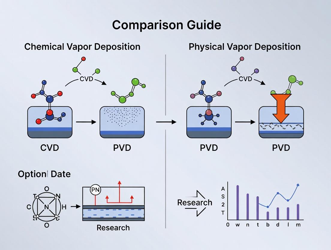
CVD vs PVD Fundamentals: Core Principles, Mechanisms, and Material Science for Researchers
Within the context of a comprehensive CVD vs PVD comparison guide for advanced manufacturing, this technical guide deconstructs the fundamental atomic-level process mechanisms of Chemical Vapor Deposition (CVD) and Physical Vapor Deposition (PVD). Aimed at researchers and development professionals in fields requiring precise thin-film coatings, this document provides an in-depth analysis of the reaction kinetics, transport phenomena, and nucleation events that define each technology. The mechanisms are framed by their implications for film properties critical to applications such as medical device coatings and semiconductor fabrication.
Atomic-Level Mechanisms of Chemical Vapor Deposition (CVD)
CVD is a process where a solid thin film is deposited onto a substrate via the chemical reaction of vapor-phase precursors. The mechanism occurs through a sequential, surface-mediated pathway.
Core Process Steps & Mechanisms
The deposition process follows a series of interdependent steps, each governed by specific physical and chemical principles.
Diagram 1: Sequential atomic-level steps in a generic CVD process.
1. Gas Phase Transport & Precursor Delivery: Precursor molecules (e.g., SiH₄, TiCl₄) are transported in a carrier gas (H₂, Ar) to the substrate surface. This is a convective and diffusive process, often modeled by boundary layer theory.
2. Adsorption: Precursor molecules physically adsorb (physisorb) onto the heated substrate surface via weak van der Waals forces. This may be followed by chemisorption, where stronger chemical bonds form, dissociating the precursor (e.g., SiH₄ → SiH₂* + H₂, where * denotes a surface species).
3. Surface Diffusion & Reaction: The adsorbed species diffuse across the surface until they encounter reactive sites. Heterogeneous chemical reactions then occur, incorporating the film material (e.g., Si from SiH₄) into the growing lattice. Key reactions include pyrolysis, reduction, and hydrolysis.
4. Nucleation & Film Growth: Stable clusters (nuclei) form on the substrate. The growth mode (Frank-van der Merwe/layer-by-layer, Volmer-Weber/island, or Stranski-Krastanov) depends on the interfacial energies between substrate, film, and vapor.
5. Byproduct Desorption & Removal: Volatile reaction byproducts (e.g., HCl, H₂O, excess H₂) desorb from the surface and are transported away by the gas flow.
Experimental Protocol for Analyzing CVD Mechanisms (In Situ QCM)
Objective: To measure real-time adsorption and growth kinetics during a CVD process. Method: Quartz Crystal Microbalance (QCM) integrated into a CVD reactor.
- Setup: A gold-coated quartz crystal oscillator (sensor) is installed as the substrate in the reactor. It is connected to a frequency counter via electrical feedthroughs.
- Calibration: The fundamental resonance frequency (f₀ ~5 MHz) is established under vacuum or inert gas at the deposition temperature. The Sauerbrey equation (Δf = -Cf · Δm) is calibrated, where Cf is the mass sensitivity constant.
- Experiment: Precursor gases are introduced at controlled partial pressures. The frequency shift (Δf) is monitored in real-time.
- Data Analysis: The frequency decrease is directly proportional to mass increase. The derivative (d(Δf)/dt) provides the instantaneous deposition rate. Changes in slope indicate transitions between adsorption-limited and diffusion-limited regimes.
Key Quantitative Parameters for CVD
Table 1: Key Quantitative Parameters Governing Atomic-Level CVD Mechanisms
| Parameter | Typical Range/Value | Influence on Atomic Mechanism |
|---|---|---|
| Deposition Temperature | 200°C – 1200°C | Governs reaction kinetics, surface diffusion, and precursor decomposition. |
| Chamber Pressure | 0.1 Pa (LP-CVD) – 10⁵ Pa (AP-CVD) | Affects gas-phase reaction likelihood, mean free path, and boundary layer thickness. |
| Precursor Partial Pressure | 1 – 1000 Pa | Drives adsorption rate (often 1st order). |
| Activation Energy (Eₐ) | 0.5 – 3 eV | Determines temperature sensitivity of the surface reaction rate. |
| Sticking Coefficient (s) | 10⁻⁶ – 1 | Probability of adsorption per collision; indicates precursor reactivity. |
Atomic-Level Mechanisms of Physical Vapor Deposition (PVD)
PVD involves the physical ejection of atoms from a solid source (target) and their subsequent condensation onto a substrate. The mechanism is primarily physical rather than chemical.
Core Process Steps & Mechanisms
The primary PVD techniques are evaporation and sputtering, each with distinct atom-generation mechanisms but similar condensation physics.
Diagram 2: Atomic-level steps in a generic PVD (sputtering) process.
1. Target Erosion (Atom Generation): * Evaporation: The solid source is heated (resistively, by electron beam) above its melting point. Atoms gain sufficient kinetic energy to overcome the binding energy (enthalpy of sublimation, ΔH_sub) and enter the vapor phase. * Sputtering: A plasma of inert gas ions (Ar⁺) is accelerated into the target cathode. Momentum transfer from incident ions to target atoms ejects (sputters) target atoms if the transferred energy exceeds the surface binding energy (~3-5 eV).
2. Vapor/Plasma Transport: Ejected atoms travel through the vacuum or low-pressure plasma environment toward the substrate. In sputtering, the atoms may undergo gas-phase collisions (scattering), which is influenced by pressure and target-substrate distance.
3. Substrate Collision & Condensation: Atoms (now "adatoms") impinge on the substrate, transferring their kinetic energy. They may physisorb if they lose sufficient energy to the substrate lattice.
4. Adatom Surface Diffusion: Adatoms migrate across the surface with a diffusivity Ds ∝ exp(-Ediff / kT), where E_diff is the surface diffusion activation energy. This is a critical step for finding low-energy lattice sites.
5. Nucleation, Island Growth, and Coalescence: Adatoms meet to form stable nuclei. Islands grow three-dimensionally (Volmer-Weber mode is common for metals on insulators) until they impinge and coalesce to form a continuous film.
Experimental Protocol for Sputter Yield Measurement
Objective: To quantify the number of atoms ejected per incident ion, a fundamental parameter for sputtering mechanisms. Method: Weight loss measurement of a target in a calibrated sputtering system.
- Target Preparation: A high-purity target disc is precisely cleaned, dried, and weighed on a microbalance (accuracy ±0.001 mg).
- Sputtering: The target is installed as the cathode in a magnetron sputter system. The system is pumped to base pressure (<10^-4 Pa). High-purity Ar is introduced at a fixed pressure (e.g., 0.5 Pa). A constant current/power is applied for a precisely measured time.
- Collection (Optional): A collector plate can be positioned to capture ejected material for complementary analysis.
- Post-Experiment Analysis: The target is re-weighed. The mass loss (Δm) is converted to atoms lost using atomic weight and Avogadro's number. The total ion flux to the target is calculated from the measured current (I) and time (t): #Ions = (I * t) / (e * γ), where e is electron charge and γ is the secondary electron emission coefficient. Sputter Yield (Y) = (#Atoms Removed) / (#Incident Ions).
Key Quantitative Parameters for PVD
Table 2: Key Quantitative Parameters Governing Atomic-Level PVD Mechanisms
| Parameter | Typical Range/Value | Influence on Atomic Mechanism |
|---|---|---|
| Sputter Yield (Y) | 0.1 – 2 atoms/ion (for Ar⁺) | Determines erosion rate; depends on ion energy, mass, and target binding energy. |
| Adatom Surface Diffusion Energy (E_diff) | 0.1 – 1.0 eV | Controls island density and microstructure; higher E_diff leads to smaller grains. |
| Incident Particle Energy | 0.1 eV (evap.) – 10s eV (sputt.) | Affects film density and residual stress; higher energy promotes densification. |
| Substrate Temperature (Ts / Tm) | 0.2 – 0.5 (T_m in Kelvin) | Governs adatom mobility and recrystallization processes. |
| Working Pressure | 10^-4 Pa (evap.) – 1 Pa (sputt.) | Controls mean free path and scattering during transport. |
The Scientist's Toolkit: Essential Research Reagent Solutions
Table 3: Key Materials and Reagents for Investigating CVD/PVD Mechanisms
| Item | Function & Relevance |
|---|---|
| High-Purity Precursor Gases (e.g., SiH₄, TiCl₄, WF₆) | Source of depositing material in CVD; purity dictates reaction pathways and impurity levels in the film. |
| Inert Carrier/Plasma Gases (e.g., 99.999% Ar, N₂, H₂) | Transport medium (CVD) or sputtering agent (PVD). H₂ can act as a reducing agent in CVD. |
| Single-Crystal Substrates (e.g., Si(100), SiO₂, Al₂O₃) | Well-defined surfaces for fundamental studies of nucleation, growth modes, and epitaxy. |
| Calibrated Mass Flow Controllers (MFCs) | Precisely regulate precursor and gas flows, enabling kinetic studies and reproducible conditions. |
| In Situ Diagnostics (QCM, Ellipsometer, RGA) | Quartz Crystal Microbalance (mass), Spectroscopic Ellipsometry (thickness/optics), Residual Gas Analyzer (gas species) for real-time mechanism analysis. |
| High-Purity Sputtering Targets (e.g., Ti, Al, Pt, SiO₂) | Source material for PVD; purity and microstructure affect ejection mechanism and film properties. |
| Surface Analysis Reagents (e.g., XPS calibration standards, TEM grid substrates) | Materials needed to prepare and analyze samples post-deposition to deduce growth history and chemistry. |
Table 4: Atomic-Level Comparison of CVD vs. PVD Core Mechanisms
| Feature | Chemical Vapor Deposition (CVD) | Physical Vapor Deposition (PVD) |
|---|---|---|
| Driving Force | Chemical potential gradient & reaction thermodynamics. | Supersaturation of vapor phase. |
| Primary Energy Input | Thermal (substrate heating). | Kinetic (evaporation heat or ion bombardment). |
| Growth Species | Reactant molecules, radicals, and adatom complexes. | Atomic or ionic species. |
| Reaction Locus | Primarily on substrate surface (heterogeneous). | At target (erosion) and substrate (condensation). |
| Conformal Coverage | Excellent, due to surface-mediated reactions and gas-phase diffusion. | Line-of-sight limited; poor step coverage without substrate rotation/plasma. |
| Typical Deposition Rate | 1 – 1000 nm/min (highly variable). | 1 – 100 nm/min. |
| Film Density & Stress | Can be tailored; often tensile. | Can be very dense; often compressive due to peening effect (sputtering). |
| Key Controlling Parameter | Temperature (activates reactions). | Pressure & Power (control flux and energy). |
The selection between CVD and PVD for advanced applications is fundamentally rooted in their divergent atomic-level mechanisms. CVD, governed by thermally activated surface chemistry, excels at producing uniform, conformal films with complex stoichiometries. PVD, driven by physical ejection and condensation, offers precise control over the energy and flux of depositing species, leading to dense, high-purity metallic or simple compound films. This mechanistic understanding provides the essential framework for researchers to rationally select, optimize, and innovate deposition processes for specific technological needs in drug delivery systems, implantable devices, and microelectronics.
Within the comprehensive evaluation of Chemical Vapor Deposition (CVD) versus Physical Vapor Deposition (PVD) for advanced material synthesis, a critical analysis of material inputs and their resultant outputs is paramount. This guide details the core precursors, target materials, and the direct causal relationships to final thin-film properties, providing a framework for researchers and development professionals to optimize deposition processes for specific applications, including specialized coatings for biomedical devices and sensor platforms.
Core Material Inputs: Precursors and Targets
The choice of input material defines the fundamental chemistry and physics of the deposition process, creating a divergence between CVD and PVD methodologies.
Chemical Vapor Deposition (CVD) Precursors
CVD relies on volatile precursors that undergo chemical reactions on the substrate surface. Key classes include:
- Metalorganics: (e.g., Trimethylaluminum [TMA], Tetraethylorthosilicate [TEOS]) for oxides.
- Hydrides: (e.g., Silane [SiH₄], Ammonia [NH₃]) for semiconductors and nitrides.
- Metal Halides: (e.g., Tungsten Hexafluoride [WF₆], Titanium Tetrachloride [TiCl₄]) for refractory metals and ceramics.
- Metal-organic Complexes: For advanced Atomic Layer Deposition (ALD) processes.
Physical Vapor Deposition (PVD) Targets
PVD utilizes solid-source targets that are physically dislodged via kinetic energy.
- Elemental Targets: High-purity (99.95-99.999%) metals (e.g., Ti, Al, Cu, Ag) or non-metals (e.g., C, Si).
- Alloy Targets: Pre-alloyed materials (e.g., Ti6Al4V, CoCrMo) for specific stoichiometries.
- Compound/Ceramic Targets: Sintered compounds (e.g., TiO₂, SiO₂, ITO, Al₂O₃).
Quantitative Input-Output Relationships
The following tables summarize the direct influence of key inputs and process parameters on critical thin-film properties, based on current literature and experimental data.
Table 1: CVD Process: Key Precursors and Resultant Film Properties
| Precursor (Input) | Co-reactant | Process Type | Primary Film Output | Key Film Properties & Influencing Parameters |
|---|---|---|---|---|
| Trimethylaluminum (TMA) | H₂O, O₂, NH₃ | Thermal/Plasma-ALD/PE-CVD | Al₂O₃, AlN | Dielectric Constant (~9), Breakdown Strength (>10 MV/cm). Growth per cycle (GPC) ~1.1 Å (TMA/H₂O ALD). Stress tunable by temp. and plasma power. |
| Tetraethylorthosilicate (TEOS) | O₂, O₃ | LPCVD, PECVD | SiO₂ | Conformality >95% (excellent step coverage). Refractive Index (~1.46). Wet etch rate controlled by density/carbon content. |
| Tungsten Hexafluoride (WF₆) | H₂, SiH₄ | LPCVD | Tungsten (W) | Resistivity (9-15 μΩ·cm). Step coverage highly dependent on nucleation and deposition regime (reaction vs. diffusion limited). |
| Ammonia (NH₃) | TMA, TiCl₄ | PECVD, Thermal CVD | AlN, TiN | AlN: Piezoelectric Coefficients (d₃₃ ~5.5 pC/N). Crystallinity and stress heavily dependent on substrate temp. and plasma conditions. |
Table 2: PVD Process: Target Materials and Resultant Film Properties
| Target Material (Input) | Deposition Technique | Primary Film Output | Key Film Properties & Influencing Parameters |
|---|---|---|---|
| Titanium (Ti) | DC Magnetron Sputtering | Metallic Ti, TiN (with N₂ gas) | Ti Adhesion Layer: Stress (>1 GPa compressive typical). Microstructure (columnar). TiN: Hardness (~25 GPa), Resistivity (~100 μΩ·cm). |
| Silver (Ag) | DC Magnetron Sputtering | Ag, Ag-alloys | Low Resistivity (~2 μΩ·cm). Surface roughness and grain size critical for optical/conductive performance. Susceptible to oxidation. |
| Indium Tin Oxide (ITO) | RF Magnetron Sputtering | ITO (Transparent Conductor) | Optical Transparency (>85% vis), Resistivity (low 10⁻⁴ Ω·cm). Properties highly sensitive to O₂ partial pressure and substrate temperature during deposition. |
| Titanium Dioxide (TiO₂) | Reactive Sputtering (Ti target + O₂) | TiO₂ (Anatase, Rutile) | Refractive Index (~2.4-2.7), Photocatalytic Activity. Phase and crystallinity controlled by substrate bias, temperature, and post-annealing. |
Experimental Protocols for Key Characterizations
To establish the relationships in Tables 1 & 2, standardized experimental protocols are essential.
Protocol: Measuring Thin-Film Stress via Wafer Curvature (Stoney's Formula)
Objective: Determine intrinsic stress of a deposited film. Materials: Single-side polished Si wafer, deposition system, surface profilometer or interferometer. Method:
- Measure the radius of curvature (R_sub) of the bare substrate using a profilometer scan across its diameter.
- Deposit the thin film uniformly on the substrate.
- Measure the new radius of curvature (R_film+sub).
- Calculate the film stress (σf) using Stoney's equation:
σ_f = (E_s / (6(1-ν_s))) * (t_s² / t_f) * ((1/R_film+sub) - (1/R_sub))where Es is substrate Young's modulus, νs is substrate Poisson's ratio, ts is substrate thickness, t_f is film thickness.
Protocol: Four-Point Probe Resistivity Measurement
Objective: Determine the sheet resistance and resistivity of a conductive film. Materials: Four-point probe head with linear, equidistant tips, current source, voltmeter, film on insulating substrate. Method:
- Place the probe tips in direct, colinear contact with the film surface.
- Apply a known constant current (I) between the outer two probes.
- Measure the voltage drop (V) between the inner two probes.
- Calculate sheet resistance (R_s): For a thin film much thinner than the probe spacing (s), and on an insulating substrate:
R_s = (π/ln2) * (V/I) ≈ 4.532 * (V/I). - Calculate resistivity (ρ):
ρ = R_s * t_f, where t_f is the film thickness.
Process and Property Relationship Visualizations
CVD: Precursor Chemistry to Film Properties
PVD: Energetics Determine Microstructure & Properties
The Scientist's Toolkit: Essential Research Reagent Solutions
Table 3: Key Reagents and Materials for Thin-Film Research & Analysis
| Item | Function/Application | Key Consideration |
|---|---|---|
| High-Purity Precursors (e.g., TMA, DEZ in CVD/ALD bubbler) | Source material for film growth. Dictates final film composition and purity. | Must be ultra-high purity (>99.999%), moisture/oxygen-free handling to prevent pre-reaction. Delivery rate controlled by bubbler temp. & carrier gas flow. |
| Sputtering Targets (4", 6" dia., planar or rotary) | Solid source material for PVD. Composition defines film stoichiometry directly. | Purity (typically 99.95-99.999%), density (>95% theoretical), bonding integrity to backing plate. Alloy targets require uniform composition. |
| Process Gases (Ar, N₂, O₂, H₂, NF₃) | Carrier, reactive, or plasma generation gases. Critical for film chemistry and deposition kinetics. | Must be research grade (99.999%+) with dedicated, clean plumbing. Reactive gases require precise mass flow control and safety systems. |
| Standard Reference Substrates (Si wafers, SiO₂/Si, glass slides) | Provides a consistent, well-characterized surface for deposition and subsequent analysis. | Surface finish (polished, roughness), crystallographic orientation, cleanness (RCA clean standard), and thermal properties. |
| Ellipsometry Reference Samples (SiO₂ on Si, known thickness) | Used to calibrate and validate thickness and optical constant measurement tools. | Certified thickness and refractive index from a standards body (e.g., NIST) or reliable supplier. |
| Etchants & Diluents (BOE, HF, AZ 400K developer, solvents) | For patterning, lift-off, post-deposition etching, and equipment cleaning. | Solution purity, concentration stability, and compatibility with film/substrate. Requires strict safety protocols (HF especially). |
The Role of Thermodynamics and Kinetics in CVD and PVD Deposition
Within the ongoing research on Chemical Vapor Deposition (CVD) versus Physical Vapor Deposition (PVD) for advanced material synthesis, a fundamental understanding of the governing principles is essential. This whitepaper provides an in-depth technical analysis of the roles of thermodynamics and kinetics in these two dominant thin-film deposition technologies. While both aim to produce high-quality coatings, their operational principles, dictated by these core scientific disciplines, diverge significantly, influencing their applicability in fields ranging from semiconductor manufacturing to biomedical device coating.
Thermodynamic Foundations
Thermodynamics determines the feasibility, direction, and equilibrium state of a deposition process. It answers whether a reaction can happen.
Thermodynamics in CVD
CVD is a chemically driven process where gaseous precursors react or decompose on a heated substrate to form a solid film. Thermodynamics is paramount.
- Gibbs Free Energy (ΔG): The primary driver. For deposition to be spontaneous, ΔG must be negative (ΔG < 0). ΔG = ΔH - TΔS, where ΔH is enthalpy change, T is temperature, and ΔS is entropy change. Deposition typically results in a decrease in entropy (ΔS < 0), making high temperature necessary to achieve a negative ΔG for many reactions.
- Equilibrium Constants: Govern the partial pressures of reactants and products at the substrate surface. The process is often operated in a regime controlled by chemical equilibrium.
- Phase Stability: Thermodynamic phase diagrams predict which phase (e.g., diamond vs. graphite in carbon CVD) will be deposited under given temperature and pressure conditions.
Thermodynamics in PVD
PVD is a physical process involving the transition of material from a condensed phase (solid or liquid source) to a vapor phase and back to a condensed phase (film) on the substrate. Thermodynamics plays a different role.
- Vapor Pressure: The key thermodynamic property. The source material must be heated (or sputtered) to achieve a sufficient vapor pressure for effective transfer. The Clausius-Clapeyron equation describes this relationship.
- Surface Energy: Thermodynamics of film nucleation and growth are influenced by the surface and interfacial energies between the film, substrate, and any ambient gas. This affects adhesion and film morphology.
- Heats of Sublimation/Vaporization: The energy required for the phase change from solid/liquid to vapor dictates the energy input needed at the source.
Table 1: Thermodynamic Parameters Comparison
| Parameter | Role in CVD | Role in PVD | Typical Values/Considerations |
|---|---|---|---|
| Gibbs Free Energy (ΔG) | Primary driver for reaction feasibility. Must be <0. | Indirect role; relates to surface diffusion & nucleation. | CVD: ΔG can range from -50 to -300 kJ/mol for common reactions. |
| Enthalpy (ΔH) | Heat of reaction; exothermic reactions are common. | Heat of vaporization/sublimation for source material. | PVD (Evap.): ΔH_sub for Ti ~425 kJ/mol. |
| Entropy (ΔS) | Usually negative; gas → solid transition. Order increases. | Negative for condensation; positive for vaporization. | CVD: ΔS typically -100 to -200 J/(mol·K). |
| Equilibrium Constant (K) | Directly controls gas-phase composition at substrate. | Not applicable in the same sense; process is far from equilibrium. | CVD: K > 1 for feasible deposition. |
| Vapor Pressure | Influences precursor delivery and by-product removal. | Critical: Determines source evaporation/sputtering rate. | PVD: Must reach ~10⁻² Torr for usable evaporation rate. |
Kinetic Principles
Kinetics describes the rate and pathway of the deposition process. It determines how fast the thermodynamically feasible process occurs and often controls the final film's microstructure.
Kinetics in CVD
CVD involves multiple sequential and parallel kinetic steps:
- Gas-Phase Transport: Reactants diffuse through a boundary layer to the substrate.
- Adsorption: Reactants adsorb onto the substrate surface.
- Surface Reactions: Chemical reactions occur (decomposition, reaction, reduction).
- Desorption: Gaseous by-products desorb.
- Diffusion of By-Products: By-products diffuse away from the substrate.
The slowest of these steps is the rate-limiting step. At high temperatures, surface reaction kinetics are fast, and the process is often mass-transport limited. At lower temperatures, it becomes surface-reaction-rate limited.
Kinetics in PVD
PVD kinetics are governed by physical processes:
- Vapor Generation: Rate of atom ejection from the target (via thermal evaporation or plasma sputtering).
- Transport: Line-of-sight or collision-dominated travel of vapor to the substrate.
- Condensation & Nucleation: Atoms impinge, diffuse, and nucleate on the substrate surface.
- Film Growth: Nuclei coalesce and film thickens via continued atom deposition and surface diffusion.
The energy of the arriving species (a few tenths of an eV in evaporation to tens of eV in sputtering) critically influences surface diffusion, nucleation density, and film density.
Table 2: Kinetic Rate-Limiting Steps & Controlling Parameters
| Process | Common Rate-Limiting Step | Key Kinetic Control Parameters | Effect on Film Properties |
|---|---|---|---|
| Atmospheric-Pressure CVD | Mass transport of precursors through boundary layer. | Gas flow hydrodynamics, reactor geometry, total pressure. | Conformal coverage, growth rate uniformity. |
| Low-Pressure CVD (LPCVD) | Surface reaction kinetics. | Substrate temperature, precursor partial pressure. | High uniformity, excellent step coverage, columnar grain structure. |
| Plasma-Enhanced CVD (PECVD) | Radical generation & surface reactions. | Plasma power, frequency, precursor chemistry. | Low-temperature deposition, altered film stoichiometry/stress. |
| Thermal Evaporation | Vaporization rate at the source. | Source temperature (Boiling point), source-substrate distance. | High purity, porous/columnar structure if substrate is cold. |
| Magnetron Sputtering | Sputter yield at the target. | Argon pressure, applied power, magnetic field strength. | Dense films, good adhesion, controllable stress via bias. |
Experimental Protocols
Protocol: Determining Activation Energy for a CVD Process
Objective: To identify the surface-reaction-rate-limited regime and determine the activation energy (Eₐ) of deposition.
- Setup: Use a cold-wall, low-pressure CVD reactor with precise temperature control (±2°C) and mass flow controllers for precursors.
- Procedure: a. Set total pressure and precursor partial pressures to ensure operation in a surface-reaction-limited regime (typically low pressure, high dilution). b. Deposit films over a temperature range (e.g., 400-600°C) while keeping all other parameters constant. c. Measure film thickness using ellipsometry or profilometry after each run. d. Calculate growth rate (Rg) in nm/min.
- Analysis: Plot ln(Rg) vs. 1/T (Arrhenius plot). The slope of the linear region is -Eₐ/R, where R is the gas constant. A high Eₐ (>50 kJ/mol) indicates a strong temperature dependence characteristic of surface-reaction control.
Protocol: Measuring Deposition Rate & Stress in a DC Magnetron Sputtering System
Objective: To characterize the kinetic dependence of a PVD process on key parameters.
- Setup: DC magnetron sputtering system with a pure metal target (e.g., Ti), substrate holder with heating/cooling and bias capability.
- Procedure: a. Load substrates (e.g., Si wafers) and establish a base pressure (<5 x 10⁻⁶ Torr). b. Introduce Argon gas and stabilize pressure (e.g., 3 mTorr). c. For rate measurement: Deposit at a fixed power (e.g., 500W) for a set time (e.g., 30 min). Measure thickness. Vary power (200W, 500W, 800W) or pressure (2, 5, 10 mTorr) systematically. d. For stress measurement: Use a wafer curvature setup (Stoney's equation) or deposit on a thin cantilever substrate and measure deflection.
- Analysis: Plot deposition rate vs. power (typically linear) and vs. pressure (often peaks at an optimal pressure). Correlate compressive/tensile stress with parameters like pressure or applied substrate bias.
CVD Deposition Kinetic Steps
PVD Deposition Kinetic Steps
The Scientist's Toolkit: Research Reagent Solutions
Table 3: Essential Materials for CVD/PVD Research
| Item | Function | Typical Examples & Notes |
|---|---|---|
| High-Purity Precursor Gases/Solutions (CVD) | Source of depositing material. Determines film composition and purity. | Silane (SiH₄) for Si; Tetraethylorthosilicate (TEOS) for SiO₂; Trimethylaluminum (TMA) for Al₂O₃. Stored in bubblers or cylinders with mass flow controllers. |
| High-Purity Target Materials (PVD) | Solid source for vapor generation. Composition defines film material. | 4N-6N purity metals (Ti, Al, Cu), alloys, or bonded ceramic targets (Al₂O₃, SiO₂). |
| Carrier/Reactive Gases | Dilute and transport precursors (CVD) or sustain plasma/sputter (PVD). | High-purity N₂, H₂, Ar. For reactive processes: O₂, NH₃, CH₄. |
| Substrates & Surface Preparants | The surface upon which the film grows. Critical for nucleation and adhesion. | Si wafers, glass slides, polished metals. Cleaning solutions: Piranha (H₂SO₄:H₂O₂), RCA-1/2, solvents (acetone, IPA). |
| Etchants/Cleaning Chemicals | For pre-deposition surface cleaning and post-deposition patterning/analysis. | Buffered Oxide Etch (BOE), hydrofluoric acid (HF) dilutions, metal etchants. |
| CVD Reactor Chamber | Controlled environment for the chemical reaction. | Hot-wall or cold-wall, quartz or stainless steel, with temperature and pressure control. |
| PVD Vacuum Chamber | High-vacuum environment for physical vapor transport. | Stainless steel chamber with diffusion/turbo pumps, achieving <10⁻⁶ Torr base pressure. |
| Energy Source | Provides activation energy for reaction (CVD) or vaporization (PVD). | Resistive/heated substrate holder (CVD), RF/DC plasma generator (PECVD, Sputtering), e-beam or resistive heater for evaporation. |
The interplay of thermodynamics and kinetics defines the core distinction between CVD and PVD. CVD is fundamentally a thermochemically driven process, where thermodynamics dictates precursor selection and reaction feasibility, and complex multi-step kinetics control growth and morphology. This often results in conformal, high-purity films but requires high temperatures or plasma activation. PVD is primarily a physicokinetic process, where thermodynamics of phase change enable vapor generation, and kinetics of atom transport and surface diffusion govern growth. It offers dense films at lower substrate temperatures but with line-of-sight limitations.
The choice for a specific application in drug development (e.g., coating medical implants, creating biosensor surfaces) or advanced research hinges on which set of thermodynamic and kinetic constraints align with the requirements for film material, substrate compatibility, microstructure, and performance.
Within the comparative framework of Chemical Vapor Deposition (CVD) vs. Physical Vapor Deposition (PVD), the evaluation of deposited thin films hinges on four critical material properties: conformality, step coverage, purity, and density. These properties directly dictate the functional performance of coatings in advanced applications, from semiconductor interconnects to biomedical device interfaces. This guide provides a technical deep-dive into these properties, their measurement, and their dependence on deposition methodology, serving as a cornerstone for informed process selection in research and development.
Property Definitions and Significance in CVD vs. PVD
Conformality & Step Coverage: These interrelated properties describe a film's ability to uniformly coat non-planar, high-aspect-ratio features. Conformality refers to the uniformity of film thickness on all surfaces, while Step Coverage quantifies the ratio of film thickness at the bottom of a feature to that on the top surface. CVD, being a surface-reaction-limited process, typically achieves superior conformality (>95%) due to the gaseous precursor's ability to diffuse into deep features. PVD, a line-of-sight process, often struggles with shadowing effects, leading to poor sidewall coverage and lower step coverage (often <50% for high-aspect-ratio trenches without advanced techniques like ionization).
Purity: This denotes the absence of contaminants (e.g., oxygen, carbon, unwanted metals) within the film. High purity is critical for electrical performance, chemical stability, and biocompatibility. CVD purity can be compromised by incomplete precursor decomposition or incorporation of ligand byproducts. PVD, sourcing material from a pure solid target, generally yields higher purity films, though contamination from the chamber environment (e.g., residual gases) remains a risk.
Density: Film density (mass per unit volume) impacts mechanical strength, diffusion barrier performance, and corrosion resistance. Dense films have fewer voids or columnar microstructures. High-density PVD films (e.g., via sputtering) are common due to high particle energy. CVD films can vary from porous (at low temperature) to highly dense (at high temperature or using plasma enhancement), with density closely tied to deposition kinetics and precursor chemistry.
Table 1: Comparison of Typical Property Ranges for CVD vs. PVD Processes
| Property | Typical CVD Range | Typical PVD (Sputtering) Range | Key Influencing Deposition Parameters |
|---|---|---|---|
| Step Coverage | 80% - 100%+ (Excellent) | 10% - 50%* (Poor to Moderate) | CVD: Precursor pressure, reactivity, temp. PVD: Target-substrate geometry, bias, pressure. |
| Film Purity | 95% - 99.999% (Precursor-dependent) | 99.9% - 99.999% (Target-dependent) | CVD: Precursor purity, decomposition temp., carrier gas. PVD: Base pressure, target purity, sputter gas purity. |
| Film Density | Moderate to Very High (1.5 - 19+ g/cm³) | High to Very High (2.7 - 19+ g/cm³) | CVD: Deposition temp., pressure, plasma assist. PVD: Sputter power, bias voltage, substrate temp. |
| Typical Deposition Rate | 1 - 1000 nm/min | 5 - 200 nm/min | CVD: Precursor flow, temp. PVD: Sputter yield, power. |
*Can be improved to >80% with techniques like Ionized PVD (I-PVD).
Table 2: Experimental Measurement Techniques for Critical Properties
| Property | Primary Measurement Technique | Brief Protocol Summary |
|---|---|---|
| Step Coverage | Cross-Sectional Scanning Electron Microscopy (SEM) | 1. Deposit film on patterned wafer with trenches/vias. 2. Cleave wafer to expose cross-section. 3. Image with SEM. 4. Measure film thickness at top, sidewall, and bottom. Calculate ratio: (Thicknessbottom / Thicknesstop) x 100%. |
| Purity | Secondary Ion Mass Spectrometry (SIMS) / X-ray Photoelectron Spectroscopy (XPS) | SIMS: 1. Mount sample in UHV chamber. 2. Erode surface with primary ion beam (e.g., Cs+, O2+). 3. Analyze ejected secondary ions via mass spectrometer. 4. Quantify elemental impurities using standard reference materials. |
| Density | X-ray Reflectivity (XRR) / Ellipsometric Porosimetry | XRR: 1. Direct a collimated X-ray beam at grazing incidence onto film. 2. Measure reflected intensity vs. incident angle (θ). 3. Model the critical angle and interference fringes (Kiessig fringes) to extract electron density profile, which correlates with mass density. |
Detailed Experimental Protocols
Protocol 4.1: Measuring Step Coverage via SEM
Objective: Quantify the step coverage of a SiO2 film deposited via Plasma-Enhanced CVD (PECVD) on a silicon trench structure.
Materials & Equipment:
- Patterned silicon wafer with trenches (e.g., 100 nm width, 200 nm depth).
- PECVD system.
- Cleaving tool and tweezers.
- Field-Emission Scanning Electron Microscope (FE-SEM).
- Conductive coating system (sputter coater for Au/Pd).
Methodology:
- Deposition: Load the patterned wafer into the PECVD chamber. Deposit 50 nm of SiO2 using silane (SiH4) and nitrous oxide (N2O) precursors at 300°C.
- Sample Preparation: Using a diamond scribe and cleaving tool, carefully cleave the wafer to create a clean cross-section through the trenches. Handle samples with tweezers at the edges only.
- SEM Preparation: Mount the cleaved sample on an SEM stub with conductive tape. Sputter-coat with a 5 nm layer of Au/Pd to prevent charging.
- Imaging & Measurement: Insert the stub into the FE-SEM. Image the cross-section at 100,000-200,000x magnification. Use the SEM's measurement software to record:
- T: Film thickness on the planar top surface.
- B: Film thickness at the bottom of the trench.
- S: Film thickness on the sidewall (midpoint).
- Calculation: Step Coverage (%) = (B / T) * 100%. Conformality can be assessed by comparing S to T.
Protocol 4.2: Determining Film Density via X-Ray Reflectivity (XRR)
Objective: Determine the density and thickness of a titanium nitride (TiN) film deposited by reactive sputtering (PVD).
Materials & Equipment:
- TiN film on a smooth silicon substrate.
- X-ray diffractometer equipped with reflectometry stage.
- Modeling software (e.g., REFS, Leptos).
Methodology:
- Sample Loading: Place the sample on the XRR stage, ensuring it is level.
- Alignment: Align the sample surface to intersect the X-ray beam (Cu Kα, λ=1.5406 Å) at near-zero angle.
- Data Acquisition: Perform a θ-2θ scan from 0° to 5° or higher (depending on film thickness) with a very small step size (e.g., 0.005°). Measure the reflected X-ray intensity.
- Modeling & Fitting:
- Import the experimental data (angle vs. intensity) into modeling software.
- Construct a model layer stack: Si substrate / native SiO2 interface / TiN film / surface roughness layer.
- Input initial guesses for layer thickness, density, and roughness.
- Run a fitting algorithm to minimize the difference between the simulated and experimental curves by adjusting parameters.
- Analysis: The critical angle (θ_c) is directly related to the film's electron density. The fitted density (in g/cm³) and thickness (in nm) are the primary outputs. The periodicity of the Kiessig fringes provides thickness validation.
Visualizations
Diagram 1: Deposition Process Influence on Step Coverage
Diagram 2: Workflow for Characterizing Film Purity & Density
The Scientist's Toolkit: Research Reagent Solutions
Table 3: Essential Materials for Thin Film Deposition & Characterization
| Item / Reagent | Primary Function in Experiments | Key Considerations for CVD/PVD Research |
|---|---|---|
| High-Purity Solid Targets (PVD) | Source material for sputtering or evaporation (e.g., Ti, Al, Pt, SiO2). | Purity (99.99%-99.9999%), bonding quality to backing plate, grain structure. |
| Metalorganic/Precursor Gases (CVD) | Chemical source for film constituents (e.g., TEOS for SiO2, TMA for Al2O3). | Vapor pressure, decomposition temperature, reactivity/stability, impurity levels. |
| High-Purity Process Gases | Carrier gas (Ar, N2), reactive gas (O2, N2, NH3), or purge gas. | Moisture and oxygen levels (<1 ppm), consistent flow control via Mass Flow Controllers (MFCs). |
| Patterned Test Wafers | Substrates with trenches, vias, or planar areas for step coverage and film property evaluation. | Feature dimensions (width, depth, aspect ratio), surface chemistry (Si, SiO2, etc.). |
| Standard Reference Materials (SRM) | Certified thin films (e.g., SiO2 on Si of known thickness/density) for instrument calibration. | Traceability to NIST or other standards, certified property values (thickness, density). |
| Conductive Coatings (Au/Pd, C) | Applied to insulating samples prior to SEM imaging to prevent charging artifacts. | Thickness control (too thick masks details), uniformity, choice of coating material. |
The selection of coating deposition technology—Chemical Vapor Deposition (CVD) or Physical Vapor Deposition (PVD)—is fundamental to the performance of advanced biomedical devices. CVD involves the chemical reaction of gaseous precursors on a substrate, typically producing highly conformal, uniform coatings well-suited for complex geometries. PVD involves the physical transfer of material from a target to a substrate via sputtering or evaporation, offering precise control over composition, density, and crystallinity at lower temperatures. This whitepaper details how each technique is optimized for three critical applications, with performance data directly attributable to the deposition method.
Drug-Eluting Stents (DES)
DES combine a metallic stent scaffold with a polymeric coating that elutes a therapeutic drug to inhibit neointimal hyperplasia and restenosis.
Coating Technologies & Performance
The coating architecture—typically a drug-polymer matrix on a primer layer—demands exceptional adhesion, biocompatibility, and controlled release kinetics.
Table 1: CVD vs. PVD for DES Primer/Barrier Layers
| Parameter | CVD (e.g., parylene-C) | PVD (e.g., SiOx, TaOx) |
|---|---|---|
| Conformality | Excellent (>95% step coverage) | Moderate to Good (line-of-sight) |
| Coating Density | Moderate | High, Dense |
| Deposition Temp. | Low to Moderate (~25-150°C) | Low (<100°C possible) |
| Primary Function | Biostable barrier, corrosion protection | Hemocompatible layer, drug diffusion barrier |
| Adhesion to Metal | Good (mechanical interlocking) | Excellent (metallurgical bonding) |
| Key Advantage | Uniform coating on intricate struts | Precise control of stoichiometry & crystallinity |
Experimental Protocol: In-Vitro Drug Release Kinetics
- Objective: Quantify drug (e.g., sirolimus, paclitaxel) elution profile from a PVD-coated vs. CVD-coated DES.
- Materials: DES samples (n=5 per group), phosphate-buffered saline (PBS) with 0.05% Tween 80 (sink condition), HPLC vials.
- Method:
- Each DES is placed in a sealed container with 10 mL of release medium at 37°C.
- At predetermined intervals (1h, 6h, 1, 2, 4, 7, 14, 28 days), the entire medium is withdrawn and replaced with fresh pre-warmed medium.
- The collected medium is analyzed via High-Performance Liquid Chromatography (HPLC) to determine drug concentration.
- Cumulative drug release is plotted vs. time. The release rate constant (k) is calculated by fitting to mathematical models (e.g., Higuchi).
- Outcome: PVD-generated ceramic layers often demonstrate more linear, sustained release profiles compared to polymer-based CVD coatings due to differences in diffusion pathways.
Diagram Title: In-Vitro Drug Release Assay Workflow
Implant Coatings
Coatings on orthopedic (hips, knees) and dental implants enhance osseointegration and provide antibacterial properties.
Hydroxyapatite (HA) & Antimicrobial Coatings
Hydroxyapatite (Ca10(PO4)6(OH)2) coatings promote bone ingrowth. Silver or zinc-containing coatings provide antimicrobial activity.
Table 2: Deposition of HA & Antimicrobial Coatings
| Coating Type | Preferred Method | Key Process Notes | Critical Performance Metric |
|---|---|---|---|
| Crystalline HA | RF Magnetron Sputtering (PVD) | Sintering post-deposition required for crystallinity. | Crystallinity % (via XRD); Shear Adhesion Strength (>20 MPa) |
| Amorphous HA | Plasma Spray (a form of PVD) | High temperature, line-of-sight process. | Ca/P Ratio (1.67 ideal); Cohesion Integrity |
| Ag/Zn-Doped HA | Co-Sputtering (PVD) | Multiple targets (HA, Ag) allow precise dopant control. | Ion Release Profile (ICP-MS); Zone of Inhibition (vs. S. aureus) |
| Diamond-Like Carbon (DLC) | Plasma-Enhanced CVD (PECVD) | Hydrocarbon gas precursor (e.g., CH4) forms biocompatible, wear-resistant layer. | Coefficient of Friction (<0.1); Surface Energy |
Experimental Protocol: Assessment of Osteoblast Adhesion & Proliferation
- Objective: Evaluate the biocompatibility and osteoconductivity of a PVD-sputtered HA coating vs. a CVD-DLC coating.
- Materials: Coated Ti-alloy discs, MC3T3-E1 osteoblast cell line, alpha-MEM growth medium, calcein-AM live stain, fluorescence microscope.
- Method:
- Sterilize coated samples (UV light, 30 min per side).
- Seed cells at 10,000 cells/cm² onto samples in 24-well plates.
- Incubate (37°C, 5% CO2) for 1, 3, and 7 days.
- At each time point, rinse with PBS and incubate with 2 µM calcein-AM for 30 min.
- Image using fluorescence microscopy (ex/em ~495/515 nm).
- Quantify cell coverage area using image analysis software (e.g., ImageJ).
- Outcome: HA coatings typically show significantly faster and more extensive cell coverage by day 3 compared to DLC or bare titanium, indicating superior early osteoconduction.
Diagram Title: Osteoblast Adhesion and Proliferation Assay
Biosensors
Coatings functionalize sensor surfaces for the specific detection of analytes (glucose, proteins, pathogens).
Functionalization & Immobilization Layers
The sensing interface requires a thin, precise layer that immobilizes biorecognition elements (enzymes, antibodies, DNA).
Table 3: Surface Functionalization for Biosensors
| Layer Function | CVD Approach | PVD Approach | Advantage for Sensing |
|---|---|---|---|
| Reactive Primer | Silane films (e.g., APTES) via iCVD. | Sputtered Gold or Platinum thin films. | PVD provides ultra-clean, conductive surfaces for thiol-based chemistry. |
| Anti-Fouling | PEG-like coatings via parylene derivatization. | Sputtered TiO2 nanotopographies. | CVD offers uniform, pin-hole free barriers against non-specific protein adsorption. |
| Bioreceptor Attach. | Plasma polymerized acrylic acid for covalent bonding. | Not typically used for direct immobilization. | CVD creates a high-density of carboxyl groups for EDC-NHS chemistry. |
Experimental Protocol: Fabrication of a Glucose Sensor via Enzyme Immobilization
- Objective: Create a working electrode for an amperometric glucose sensor.
- Materials: Gold working electrode (PVD-sputtered), glucose oxidase (GOx) enzyme, 1-Ethyl-3-(3-dimethylaminopropyl)carbodiimide (EDC), N-Hydroxysuccinimide (NHS), 11-Mercaptoundecanoic acid (11-MUA), phosphate buffer.
- Method:
- Self-Assembled Monolayer (SAM): Immerse PVD gold electrode in 10 mM 11-MUA in ethanol for 24h to form a carboxyl-terminated SAM.
- Activation: Rinse and immerse electrode in a solution of 75 mM EDC and 15 mM NHS in water for 1 hour to activate carboxyl groups to NHS esters.
- Immobilization: Transfer electrode to a solution of 2 mg/mL GOx in phosphate buffer (pH 7.4) for 2 hours. The enzyme amine groups covalently attach to the activated esters.
- Quenching & Storage: Rinse thoroughly and store in buffer at 4°C.
- Validation: Test in glucose solutions using amperometry (+0.6V vs. Ag/AgCl); current response is proportional to glucose concentration.
- Outcome: The PVD-sputtered gold provides an atomically smooth, pure surface essential for forming a defect-free, ordered SAM, which is critical for stable enzyme loading and sensor reproducibility.
Diagram Title: Biosensor Electrode Functionalization Steps
The Scientist's Toolkit: Key Research Reagent Solutions
Table 4: Essential Materials for Coating Development & Testing
| Item | Function & Relevance |
|---|---|
| Sirolimus (Rapamycin) | Model anti-proliferative drug for DES release studies. Standard for validating coating release kinetics. |
| 11-Mercaptoundecanoic Acid (11-MUA) | Thiolated alkane chain forms ordered SAMs on PVD gold surfaces for biosensor functionalization. |
| EDC & NHS Crosslinkers | Zero-length crosslinkers for covalent immobilization of biomolecules (antibodies, enzymes) to carboxylated surfaces (common on CVD polymers). |
| Calcein-AM | Cell-permeant fluorescent dye used as a live-cell stain for quantifying adhesion and proliferation on implant coatings. |
| Simulated Body Fluid (SBF) | Ion solution mimicking human blood plasma. Used for in-vitro bioactivity testing of osteoconductive coatings (e.g., HA). |
| Phosphate Buffered Saline (PBS) with Tween 80 | Standard in-vitro release medium for hydrophobic drugs from DES, maintaining sink conditions. |
| Hydroxyapatite Sputtering Target | High-purity ceramic target for RF magnetron sputtering (PVD) of bone-integrative coatings. |
| Parylene-C Dimer | Precursor for CVD polymerization of a conformal, biostable, and barrier coating used in DES and implantable electronics. |
Advanced CVD & PVD Techniques: Method Selection and Protocol Design for Specific Applications
Within the broader paradigm of thin-film deposition for biomedical engineering, Chemical Vapor Deposition (CVD) stands as a critical counterpart to Physical Vapor Deposition (PVD). This guide provides an in-depth technical analysis of five principal CVD methodologies—APCVD, LPCVD, PECVD, ALD, and MOCVD—with a dedicated focus on their application to biomedical surfaces. The unique ability of CVD to coat complex geometries with conformal, high-purity, and functionally tailored films makes it indispensable for creating bioactive coatings, corrosion-resistant barriers, and controlled-release matrices on implants, stents, and diagnostic devices.
Fundamental Principles & Comparative Framework
All CVD techniques share a common principle: volatile precursors are transported to a substrate surface where they undergo chemical reactions to form a solid, non-volatile film. The primary differentiating factors are the energy source for the reaction (thermal, plasma) and the operational pressure regime. The choice of CVD method directly influences key film properties critical for biomedical performance: biocompatibility, adhesion, mechanical integrity, surface chemistry, and release kinetics of therapeutic agents.
The following table summarizes the core operational parameters and resultant film characteristics relevant to biomedical applications.
Table 1: Comparative Overview of CVD Methodologies for Biomedical Coatings
| Method | Pressure Range | Temperature Range (°C) | Energy Source | Key Biomedical Film Properties | Typical Biomedical Materials |
|---|---|---|---|---|---|
| APCVD | Atmospheric | 300 - 900 | Thermal | High growth rate, moderate purity & conformity. | SiO₂ (encapsulation), doped oxides. |
| LPCVD | 0.1 - 10 Torr | 500 - 900 | Thermal | Excellent uniformity, high purity, good conformity. | Poly-Si (MEMS), Si₃N₄ (barriers), stoichiometric oxides. |
| PECVD | 0.1 - 5 Torr | 100 - 400 | Plasma (RF) | Low temp., good adhesion, tunable stress & chemistry. | a-C:H (DLC), SiNₓ, SiO₂, fluorocarbon polymers. |
| ALD | < 10 Torr | 50 - 400 | Thermal/Plasma | Ultimate conformity, atomic-scale thickness control, pinhole-free. | Al₂O₃, TiO₂, ZnO (biocoatings), drug encapsulation layers. |
| MOCVD | 50 - 760 Torr | 500 - 1200 | Thermal | High-quality crystalline films, doping control. | Hydroxyapatite, GaN (biosensors), II-VI semiconductors. |
Detailed Methodologies & Biomedical Applications
Atmospheric Pressure CVD (APCVD)
Protocol: Precursor gases (e.g., SiH₄ + O₂ for SiO₂) are mixed at atmospheric pressure and passed over heated substrates in a horizontal flow reactor. Reaction is thermally driven. Biomedical Application: Primarily for rapid deposition of thick, protective silica layers on metallic substrates for preliminary corrosion barrier studies. Its simplicity is offset by lower film quality and particle contamination risks.
Low Pressure CVD (LPCVD)
Protocol: Conducted in hot-wall, vacuum-sealed tube furnaces (~1 Torr). Precursors (e.g., dichlorosilane for poly-Si) diffuse to uniformly heated substrates. Key parameters: temperature gradient, gas flow ratio, and pump-down sequence. Biomedical Application: Fabrication of micro-electro-mechanical systems (MEMS) for biosensors and implantable microdevices. LPCVD silicon nitride provides excellent, stable diffusion barriers for implant encapsulation.
Plasma-Enhanced CVD (PECVD)
Protocol: A radio-frequency (RF, typically 13.56 MHz) plasma is generated within a vacuum chamber, creating reactive radicals and ions from precursor gases (e.g., SiH₄ + NH₃ for SiNₓ). Substrate heating is minimal. Experimental Workflow: 1) Load substrate; 2) Pump to base pressure (<10 mTorr); 3) Heat to setpoint (200-350°C); 4) Introduce precursors; 5) Ignite RF plasma; 6) Deposit for timed cycle; 7) Post-deposition N₂ purge. Biomedical Application: Dominant for coating temperature-sensitive polymers and biomedical alloys. Diamond-like carbon (DLC) coatings for wear-resistant joint implants; amine-rich plasma polymers for cell adhesion.
Diagram Title: PECVD Experimental Workflow
Atomic Layer Deposition (ALD)
Protocol: A sequential, self-limiting surface reaction process. Two or more precursors are introduced in separate, alternating pulses, separated by inert gas purges (e.g., TMA + H₂O for Al₂O₃). Each cycle deposits one atomic layer. Experimental Protocol for Al₂O₃ on a Biomedical Alloy: 1) Substrate in vacuum chamber at 150°C; 2) Pulse 1: Trimethylaluminum (TMA) for 0.1s; 3) Purge: N₂ for 10s; 4) Pulse 2: H₂O vapor for 0.1s; 5) Purge: N₂ for 10s. Repeat cycle 100-200 times for desired thickness. Biomedical Application: Ultra-thin, conformal biocompatible coatings (Al₂O₃, TiO₂, ZnO) on nanoporous materials and scaffolds for controlled drug elution. Perfect barrier layers on biodegradable magnesium implants to modulate degradation.
Metalorganic CVD (MOCVD)
Protocol: Uses metalorganic precursors (e.g., trimethylgallium) and hydrides (e.g., NH₃) transported by carrier gas (H₂ or N₂) to a heated substrate where pyrolysis and reaction occur. Biomedical Application: Growth of high-quality crystalline hydroxyapatite for bone implants. Deposition of III-V (e.g., GaN) and II-VI semiconductor films for optical biosensors and bioelectronics.
The Scientist's Toolkit: Research Reagent Solutions
Table 2: Essential Materials & Reagents for CVD of Biomedical Coatings
| Item / Reagent | Function & Relevance |
|---|---|
| Silane (SiH₄) | Core precursor for silicon-based films (SiO₂, Si₃N₄, a-Si) in PECVD/LPCVD. Enables biocompatible barriers and dielectrics. |
| Ammonia (NH₃) | Nitrogen source for silicon nitride (SiNₓ) deposition. SiNₓ is a superb bio-inert diffusion barrier. |
| Acetylene (C₂H₂) | Common carbon source for PECVD deposition of Diamond-Like Carbon (DLC) coatings, providing extreme hardness and wear resistance. |
| Trimethylaluminum (TMA) | Standard aluminum precursor for ALD of Al₂O₃. Yields pinhole-free, corrosion-protective nanolayers on implants. |
| Tetraethylorthosilicate (TEOS) | Liquid precursor for LPCVD/PECVD SiO₂. Offers safer handling and smooth, conformal oxide films. |
| Calcium & Phosphorus Precursors(e.g., Ca(tmhd)₂, TMP) | Used in MOCVD for stoichiometric hydroxyapatite (Ca₁₀(PO₄)₆(OH)₂) coatings to promote osseointegration. |
| Titanium Tetrachloride (TiCl₄) | Halide precursor for ALD/PECVD of TiO₂, a photocatalytic and biocompatible oxide. |
| Hydrogen (H₂) / Nitrogen (N₂) | Carrier and purge gases. H₂ is essential for MOCVD; N₂ is a standard purge/pump-down gas for most systems. |
CVD vs. PVD in the Biomedical Context
Within the thesis of comparing vapor deposition techniques, CVD offers distinct advantages for biomedical surfaces over PVD (sputtering, evaporation):
- Superior Conformality: CVD coats complex, 3D geometries (e.g., porous scaffolds, stents) uniformly—a limitation for line-of-sight PVD.
- Versatile Chemistry: Enables deposition of complex stoichiometric compounds (e.g., hydroxyapatite) and polymer-like films.
- High-Purity & Dense Films: LPCVD and ALD produce films with excellent barrier properties against ion diffusion.
- Disadvantages: Typically involves higher temperatures (except PECVD/ALD) and hazardous precursor gases compared to PVD's solid targets.
Table 3: Quantitative Film Property Comparison: CVD vs. PVD for Biomedical Coatings
| Property | PECVD (CVD) | ALD (CVD) | Magnetron Sputtering (PVD) | Evaporation (PVD) |
|---|---|---|---|---|
| Deposition Rate (nm/min) | 10 - 500 | 1 - 10 (per cycle) | 20 - 200 | 50 - 1000 |
| Typical Coating Uniformity | Good | Excellent (atomic level) | Moderate (requires rotation) | Poor (line-of-sight) |
| Step Coverage | Conformal | Perfectly Conformal | Poor (<50% on high aspect ratio) | Very Poor |
| Film Density | Moderate to High | Very High | High | Low to Moderate |
| Adhesion to Polymers | Very Good | Good (with plasma pretreatment) | Good (with bias) | Poor |
| Operational Temperature | Low (<400°C) | Low (<400°C) | Low (can be RT) | Low (can be RT) |
Diagram Title: CVD vs PVD Selection Logic for Biomedical Coatings
The selection of a CVD methodology—APCVD, LPCVD, PECVD, ALD, or MOCVD—for biomedical surfaces is dictated by a matrix of requirements: substrate thermal stability, geometric complexity, desired film chemistry, and necessary functional performance. While PVD techniques offer advantages in low-temperature deposition of pure metals and simple compounds, the superior conformality, compositional control, and versatility of CVD make it the dominant force for advanced bioactive and protective coatings in modern biomedical device engineering. The ongoing development of novel, biocompatible precursors and hybrid CVD/PVD systems promises further innovation in this critical field.
Within the broader thesis comparing Chemical Vapor Deposition (CVD) and Physical Vapor Deposition (PVD), this guide provides an in-depth technical analysis of four principal PVD methodologies. While CVD relies on chemical reactions in the vapor phase, PVD techniques are characterized by the physical ejection of material from a source and its subsequent condensation as a thin film on a substrate. This fundamental distinction underpins differences in film purity, deposition energy, and applicability to heat-sensitive materials. The following sections detail the operational principles, quantitative performance metrics, and specific protocols for Thermal Evaporation, Sputtering, Pulsed Laser Deposition, and Cathodic Arc deposition.
Core Methodologies & Quantitative Comparison
Thermal Evaporation
Principle: Material is heated in a high vacuum until its vapor pressure is sufficient to cause sublimation or evaporation. The vapor then travels ballistically to the substrate, forming a thin film. Key Parameters: Low chamber pressure (10^-5 to 10^-7 Torr), low deposition energy (~0.1-0.5 eV). Protocol:
- Load high-purity source material (e.g., Al, Au, Ag) into a resistive boat or crucible.
- Pump chamber to base pressure of ≤ 5 x 10^-6 Torr.
- Gradually increase current through the boat to melt and then evaporate the source.
- Open the shutter to begin deposition. Monitor film thickness with a quartz crystal microbalance (QCM).
- Close shutter and cool substrate before venting chamber.
Sputtering
Principle: A plasma (typically Ar) is generated. Positive ions from the plasma are accelerated into a target (cathode), ejecting atoms via momentum transfer. These atoms condense on the substrate. Key Parameters: Higher pressure (1-100 mTorr), medium deposition energy (1-10 eV). Protocol (DC Magnetron Sputtering):
- Mount conductive target on magnetron cathode. Place substrate on anode/heater stage.
- Pump to base pressure (~10^-6 Torr). Backfill with high-purity Ar to 3-5 mTorr.
- Apply DC power (100-500 W) to ignite plasma. Pre-sputter target with shutter closed for 5-10 minutes to clean surface.
- Open shutter to deposit. Use QCM for rate control. Maintain constant pressure via a throttle valve.
Pulsed Laser Deposition (PLD)
Principle: A high-power pulsed laser ablates material from a target, creating a transient, highly energetic plasma plume that expands toward the substrate. Key Parameters: Ultra-high vacuum compatible, very high deposition energy (10-100 eV). Protocol:
- Place rotating target and substrate in vacuum chamber. Align focusing lens to illuminate target at 45°.
- Pump to base pressure (<10^-6 Torr). For oxide films, backfill with O2 to 10-200 mTorr.
- Set laser parameters (e.g., KrF excimer: 248 nm, 1-10 J/cm² fluence, 10-50 Hz repetition rate).
- Fire laser onto target. Use a rotating target to avoid pit formation. Heat substrate (often 400-800°C for complex oxides).
Cathodic Arc Deposition
Principle: A high-current, low-voltage arc is struck on a cathode target, creating small, highly ionized plasma spots. Material is ejected as mostly ions with high kinetic energy. Key Parameters: Vacuum, very high ionization fraction (~30-100%), very high energy (10-100 eV). Protocol (Filtered Cathodic Vacuum Arc - FCVA):
- Install cathode target (e.g., Ti, C) and substrate. Align magnetic filter coil.
- Pump to ~10^-5 Torr.
- Strike arc with a mechanical trigger or laser pulse, initiating a cathode spot. Maintain arc current at 50-200 A.
- Ions are guided by magnetic fields through a curved filter to remove macrodroplets. Apply substrate bias (-50 to -200 V) to control film stress and density.
Table 1: Comparative Performance Metrics of PVD Techniques
| Parameter | Thermal Evaporation | Sputtering (DC Mag.) | Pulsed Laser Deposition | Cathodic Arc |
|---|---|---|---|---|
| Typical Pressure (Torr) | 10⁻⁷ - 10⁻⁵ | 10⁻³ - 10⁻² | 10⁻⁶ - 10⁻¹ (reactive) | 10⁻⁶ - 10⁻⁴ |
| Deposition Rate (nm/min) | 10 - 1000 | 5 - 200 | 0.1 - 10 (per pulse) | 10 - 500 |
| Particle Energy (eV) | 0.1 - 1 | 1 - 10 | 10 - 100 | 10 - 100 |
| Ionization Fraction | Very Low (<1%) | Low (1-5%) | High (10-100%) | Very High (30-100%) |
| Typical Film Density | Low to Moderate | High | High | Very High |
| Step Coverage | Poor (Line-of-Sight) | Moderate (Conformal) | Poor (Line-of-Sight) | Poor (Line-of-Sight) |
| Primary Applications | Optical coatings, simple metallization | Microelectronics, decorative coatings | Complex oxides, superconductors | Hard coatings (TiN, DLC), tribological films |
The Scientist's Toolkit: Essential Research Reagents & Materials
Table 2: Key Materials for PVD Experimentation
| Item | Function | Common Examples |
|---|---|---|
| High-Purity Target/ Source | The material to be deposited as a film. | Al (4N), ITO, SiO₂, YBCO, Ti, Graphite |
| Substrate | The surface upon which the film is grown. | Si wafers, SiO₂ wafers, glass slides, MgO, LAO |
| Sputtering Gas | Inert gas to create plasma and sputter target; reactive gas to form compounds. | Argon (5N), Krypton; Oxygen (5N), Nitrogen (5N) |
| Crucible/ Boat | Holds evaporation source; must withstand high T and not react with source. | Tungsten, Molybdenum, Boron Nitride, Al₂O₃ |
| Quartz Crystal Monitor (QCM) | In-situ measurement and control of deposition rate and thickness. | 6 MHz gold-coated sensor crystal |
| Substrate Heater | Heats substrate to desired temperature to enhance adhesion and film structure. | Resistive (Ta wire), IR lamp, ceramic heater |
| Rotation & Planetary Fixtures | Ensures uniform film thickness and composition across the substrate. | Motor-driven substrate holders |
Process Visualization
Decision Logic for PVD Method Selection
Pulsed Laser Deposition Experimental Workflow
This analysis of four core PVD methodologies highlights the distinct physical mechanisms and operational envelopes that differentiate them from CVD techniques. The choice between Thermal Evaporation, Sputtering, PLD, and Cathodic Arc is governed by specific requirements for film energy, stoichiometry, density, and substrate compatibility. The quantitative data and protocols provided serve as a foundation for researchers and development professionals to select the optimal PVD technique for advanced materials synthesis, particularly in fields requiring precise control over film structure and composition without the chemical byproducts or high thermal budgets often associated with CVD.
Within the ongoing research comparing Chemical Vapor Deposition (CVD) and Physical Vapor Deposition (PVD) for advanced pharmaceutical coating applications, precise control of process parameters is paramount. This technical guide provides an in-depth analysis of the core parameters—temperature, pressure, power, and gas flow—that dictate thin-film properties, reproducibility, and ultimately, drug delivery performance. Optimization of these interdependent variables is critical for tailoring film crystallinity, adhesion, stoichiometry, and release kinetics in drug-eluting implants and nano-encapsulation.
Core Parameter Interdependence and Impact
The quality of deposited thin films in both CVD and PVD is governed by a complex interplay of physical and chemical parameters. Their optimization cannot be performed in isolation.
Quantitative Parameter Ranges and Film Effects
The following tables summarize typical operational ranges and their primary effects on film characteristics relevant to pharmaceutical coatings.
Table 1: Core Parameter Ranges for PVD (Magnetron Sputtering)
| Parameter | Typical Range | Primary Effect on Film | Relevance to Drug Coatings |
|---|---|---|---|
| Substrate Temperature | 25°C - 400°C | Adhesion, density, stress, crystallinity. | High temp can degrade heat-sensitive APIs; low temp yields porous films. |
| Chamber Pressure | 1 - 10 mTorr (Ar) | Grain size, step coverage, deposition rate. | Lower pressure yields denser, smoother barrier films for controlled release. |
| DC/RF Power | 100 - 1000 W | Deposition rate, target erosion, plasma density. | Controls coating thickness uniformity and residual film stress on implants. |
| Gas Flow (Ar) | 10 - 50 sccm | Plasma stability, sputter rate. | Primary driver of deposition kinetics; reactive gases (O₂, N₂) alter film chemistry. |
Table 2: Core Parameter Ranges for CVD (Plasma-Enhanced CVD)
| Parameter | Typical Range | Primary Effect on Film | Relevance to Drug Coatings |
|---|---|---|---|
| Substrate Temperature | 100°C - 350°C | Film conformality, chemical decomposition, residual impurities. | Enables lower temp processing for polymer/API compatibility. |
| Chamber Pressure | 0.1 - 10 Torr | Precursor mean free path, film uniformity, deposition rate. | Higher pressure improves step coverage on complex implant geometries. |
| RF Plasma Power | 50 - 500 W | Precursor dissociation, film density, ion bombardment energy. | Controls cross-linking in polymer-like films, affecting degradation rate. |
| Gas/Precursor Flow | 50 - 1000 sccm | Stoichiometry, deposition rate, precursor utilization efficiency. | Precise ratios of SiH₄/N₂O for silica barrier layers; C₂H₄ for polymer films. |
Experimental Protocols for Parameter Optimization
Protocol 1: Design of Experiments (DoE) for PVD Sputtering of TiO₂ Biocompatible Coatings
Objective: To determine the optimal combination of pressure and power for maximizing the adhesion and hydrophilicity of TiO₂ coatings on stainless steel stent substrates.
- Substrate Preparation: Clean 316L stainless steel coupons (10mm x 10mm) sequentially in ultrasonic baths of acetone, isopropanol, and deionized water for 15 minutes each. Dry under N₂ stream.
- Tool Setup: Load substrates into a magnetron sputtering chamber with a high-purity Ti target (99.99%). Evacuate base pressure to ≤ 5 x 10⁻⁶ Torr.
- DoE Matrix: Execute a full factorial design with two factors:
- RF Power: 150W, 300W, 450W.
- Working Pressure (Ar/O₂: 80/20 sccm): 3 mTorr, 6 mTorr, 9 mTorr.
- Constant parameters: Substrate temperature = 100°C, deposition time = 30 min, target-substrate distance = 60 mm.
- Deposition: Introduce Ar/O₂ gas mixture, ignite plasma, and deposit films according to the matrix.
- Characterization: Measure film adhesion via ASTM F1044 scratch test, thickness via profilometry, and contact angle using a goniometer.
- Analysis: Use response surface methodology to identify the parameter set (e.g., 300W, 6 mTorr) yielding highest adhesion strength and lowest water contact angle.
Protocol 2: Pressure-Temperature Ramp Study for PE-CVD of Silica Barrier Layers
Objective: To investigate the effect of simultaneous pressure and temperature ramping on the conformality and pinhole density of SiO₂ films on drug-loaded polymer microparticles.
- Substrate Preparation: Disperse poly(lactide-co-glycolide) (PLGA) microparticles loaded with model API (e.g., docetaxel) onto a silicon wafer carrier.
- Tool Setup: Load carrier into parallel-plate PE-CVD reactor. Evacuate to base pressure ≤ 20 mTorr.
- Process Gases: Set constant flows of SiH₄ (10 sccm) and N₂O (100 sccm).
- Ramp Procedure: Initiate a synchronized ramp profile:
- Stage 1 (0-5 min): Stabilize at 150°C and 0.5 Torr. Ignite RF plasma at 30W.
- Stage 2 (5-25 min): Ramp temperature linearly to 250°C while simultaneously ramping pressure linearly to 2.0 Torr. Maintain RF power at 30W.
- Stage 3 (25-30 min): Hold at 250°C and 2.0 Torr.
- Termination: Shut off SiH₄ flow, plasma, and heaters. Cool under continuous N₂O flow.
- Characterization: Analyze film conformality using SEM on cross-sectioned particles. Evaluate barrier property by measuring API release rate in phosphate buffer saline (PBS) vs. uncoated control using HPLC.
Visualizing Parameter Interactions and Workflows
Title: Interaction of Core Parameters in Thin Film Deposition
Title: Process Parameter Optimization Workflow
The Scientist's Toolkit: Research Reagent Solutions
Table 3: Essential Materials for CVD/PVD Pharmaceutical Coating Research
| Item | Function | Example/Specification |
|---|---|---|
| High-Purity Sputtering Targets | Source material for PVD deposition. Determines film composition. | Ti (99.995%), SiO₂, Tantalum, for biocompatible and barrier layers. |
| CVD Precursor Gases | Reactant gases or vapors that decompose to form the desired film. | SiH₄ (silane), TEOS (tetraethylorthosilicate), C₂H₄ (ethylene) for polymer films. |
| Reactive Process Gases | Modify film chemistry and properties during deposition. | O₂ (oxide formation), N₂ (nitride formation), CF₄ (for fluorocarbon films). |
| Inert Carrier/Sputter Gases | Generate plasma in PVD or carry precursor in CVD. | Argon (Ar, 99.9999%), Nitrogen (N₂, 99.999%). |
| Biocompatible Substrates | Base materials for coating deposition and testing. | 316L Stainless Steel coupons, Nitinol wires, Silicon wafers, PLGA microparticles. |
| Model Active Pharmaceutical Ingredients (APIs) | Representative drugs for release studies. | Docetaxel, Sirolimus, Fluorescein sodium (hydrophilic model). |
| Analytical Standards | For quantitative characterization of film performance. | HPLC-grade API standards, ISO 10993 biocompatibility test kits. |
| Cleaning Solvents | For critical substrate preparation to ensure adhesion. | ACS Grade Acetone, Isopropanol, and Deionized Water (18.2 MΩ·cm). |
In the context of selecting between CVD and PVD for pharmaceutical applications, optimization of temperature, pressure, power, and gas flow is not merely a procedural step but a fundamental research endeavor. CVD often offers superior conformality at lower temperatures, favorable for sensitive APIs, but requires meticulous control of gas-phase chemistry. PVD provides dense, high-purity films with excellent control over mechanical properties via energy-driven parameters. The systematic, data-driven optimization protocols outlined here provide a framework for researchers to reproducibly engineer thin-film coatings that meet the exacting demands of modern drug delivery systems, directly informing the core thesis on the comparative merits of these advanced deposition technologies.
Substrate Preparation and Surface Engineering for Enhanced Film Adhesion
Thesis Context: This whitepaper details the critical role of substrate preparation and surface engineering in thin-film deposition processes, forming a foundational technical component for a broader comparative research thesis on Chemical Vapor Deposition (CVD) versus Physical Vapor Deposition (PVD). Optimal adhesion, a prerequisite for functional performance in applications ranging from semiconductor devices to biomedical coatings, is fundamentally determined by pre-deposition surface conditions.
Core Principles of Adhesion and Surface Interactions
Film adhesion is governed by the interplay of mechanical interlocking, chemical bonding, and interfacial diffusion. The primary goal of substrate preparation is to modify surface properties to maximize these interactions. Key surface parameters include:
- Surface Energy & Wettability: A high-surface-energy substrate promotes better spreading and adhesion of the depositing film material.
- Surface Roughness: Optimal roughness increases surface area for mechanical interlocking but must be balanced against defect formation.
- Chemical State & Cleanliness: Removal of contaminants (organic, ionic, particulate) and activation of surface functional groups are essential for strong chemical bonds (e.g., covalent, ionic).
Standardized Substrate Preparation Methodologies
The following protocols are critical pre-treatments for both CVD and PVD processes.
Ultrasonic Solvent Cleaning Protocol
Objective: Remove gross organic contaminants and particulate matter.
- Materials: Substrate, beaker, ultrasonic bath, solvents (acetone, isopropanol), deionized (DI) water, nitrogen gun.
- Procedure: a. Immerse substrate in acetone, sonicate for 10 minutes at 40 kHz. b. Transfer substrate to isopropanol, sonicate for 10 minutes. c. Rinse thoroughly with flowing DI water for 2 minutes. d. Dry substrate using a filtered nitrogen gun. e. Store in a clean, dry environment or proceed immediately to next step.
RCA Standard Clean (SC-1 & SC-2) Protocol
Objective: Remove organic and ionic/metallic contaminants from silicon and other semiconductor substrates.
- Materials: DI water, ammonium hydroxide (NH₄OH, 29%), hydrogen peroxide (H₂O₂, 30%), hydrochloric acid (HCl, 37%), Teflon tanks, fume hood, hot plate.
- Procedure (SC-1 - Organic & Particle Removal): a. Prepare solution at 5:1:1 volume ratio of H₂O : H₂O₂ : NH₄OH. b. Heat to 75±5°C on a hot plate. c. Immerse substrates for 10-15 minutes. d. Rinse with copious DI water.
- Procedure (SC-2 - Ionic/Metallic Contaminant Removal): a. Prepare solution at 6:1:1 volume ratio of H₂O : H₂O₂ : HCl. b. Heat to 75±5°C. c. Immerse substrates for 10-15 minutes. d. Perform final DI water rinse and dry with nitrogen.
Plasma Surface Activation Protocol
Objective: Increase surface energy and create reactive functional groups (e.g., -OH, -COOH) via low-pressure plasma.
- Materials: Plasma cleaner, oxygen or argon gas, vacuum system.
- Procedure: a. Place cleaned substrate in plasma chamber. b. Evacuate chamber to base pressure (< 100 mTorr). c. Introduce oxygen gas at 100-500 mTorr. d. Apply RF power (50-200 W) for 30 seconds to 5 minutes. e. Vent chamber and use substrate immediately (<15 minutes) to prevent hydrophobic recovery.
Surface Engineering Techniques for Specific Adhesion Mechanisms
Adhesion Promoter Layer Deposition
Application of a thin interfacial layer to enhance chemical compatibility.
- For Metal-on-Oxide (PVD/CVD): Deposit a 5-20 nm chromium or titanium "glue layer" to bond with both oxide and the subsequent noble metal film.
- For Polymer Substrates: Apply a silane coupling agent (e.g., (3-Aminopropyl)triethoxysilane, APTES) to create a bridge between organic and inorganic phases.
Surface Roughening via Ion Beam Etching
Objective: Enhance mechanical interlocking prior to film deposition.
- Protocol: a. Place substrate in ion beam system. b. Achieve high vacuum (< 5 x 10⁻⁶ Torr). c. Introduce argon gas. d. Direct a broad-beam, low-energy (200-500 eV) Ar⁺ ion flux at a grazing incidence angle (60-80°) onto the substrate surface for 30-120 seconds. e. Transfer directly to deposition chamber under vacuum.
The efficacy of preparation methods is quantitatively assessed via adhesion tests.
Table 1: Adhesion Strength of PVD Titanium Nitride (TiN) Films under Different Pre-treatments
| Substrate (Silicon) | Pre-treatment Protocol | Adhesion Strength (Measured by Scratch Test, Critical Load Lc) | Failure Mode |
|---|---|---|---|
| As-received | Solvent wipe only | 12 ± 3 N | Complete delamination |
| Standard Clean | RCA-1 & RCA-2 | 18 ± 2 N | Partial adhesive failure |
| Engineered Surface | Ar⁺ Etch (500 eV, 60s) + Ti Glue Layer (10 nm) | 45 ± 5 N | Cohesive failure within film |
Table 2: Impact of Plasma Activation on CVD Diamond-Like Carbon (DLC) Film Adhesion
| Polymer Substrate | Plasma Treatment (Gas, Time) | Water Contact Angle (°) | Film Adhesion (Tape Test - ASTM D3359) |
|---|---|---|---|
| Polyimide (Kapton) | None | 70-75 | 0B (≥65% detached) |
| Polyimide (Kapton) | O₂, 2 min | < 10 | 4B (<5% detached) |
| Polyetheretherketone (PEEK) | Ar, 1 min | 45 | 3B (5-15% detached) |
The Scientist's Toolkit: Key Research Reagent Solutions
Table 3: Essential Materials for Substrate Preparation
| Item / Reagent | Primary Function | Technical Note |
|---|---|---|
| Piranha Solution (H₂SO₄ : H₂O₂) | Extremely powerful oxidizer for removing organics; renders surface hydrophilic. | CAUTION: Highly exothermic and explosive with organics. Use only with appropriate PPE and training. |
| Buffered Oxide Etch (BOE) (NH₄F : HF) | Selective etching of silicon dioxide to expose fresh silicon or create micro-roughness. | Controls HF activity for safer, more consistent etching rates. |
| (3-Aminopropyl)triethoxysilane (APTES) | Silane coupling agent; forms -NH₂ terminated monolayer on hydroxylated surfaces for covalent bonding. | Requires anhydrous conditions during application for monolayer control. |
| Chromium or Titanium Target (99.95+% purity) | Source material for PVD-sputtered adhesion "glue" layers. | Thin layers (5-20 nm) sufficient; thicker layers can induce stress. |
| High-Purity Argon & Oxygen Gases (99.999%) | Inert sputtering gas (Ar) and reactive gas for plasma activation/cleaning (O₂). | High purity is critical to prevent incorporation of impurities into films or interfaces. |
Process Integration & Comparative Workflow
The following diagram illustrates the decision-making workflow for surface engineering based on the deposition method (CVD vs. PVD) and substrate type.
Workflow for Surface Preparation Based on Deposition and Substrate
The following diagram contrasts the interfacial bond formation mechanisms in idealized PVD versus CVD scenarios.
Interfacial Bonding: PVD vs CVD Mechanisms
Within the broader thesis comparing Chemical Vapor Deposition (CVD) and Physical Vapor Deposition (PVD), a critical evaluation emerges through practical applications. This technical guide presents three case studies—hydrophilic coatings, antimicrobial layers, and controlled-release matrices—to elucidate the selection criteria, operational parameters, and performance outcomes of these advanced thin-film deposition techniques. The analysis provides researchers and drug development professionals with a data-driven framework for technology selection based on specific functional requirements.
Case Study 1: Hydrophilic Coatings for Medical Devices
Hydrophilic coatings reduce friction on catheters and guidewires, enhancing patient comfort and procedural success. Both CVD and PVD offer distinct pathways to achieve this.
CVD Approach: Plasma-Enhanced CVD (PECVD) is used to deposit thin, uniform films of silicon dioxide (SiO₂) or plasma-polymerized coatings rich in polar functional groups (e.g., -OH, -COOH). The reactive plasma environment enables excellent conformality on complex geometries.
PVD Approach: Reactive sputtering is employed to deposit titanium dioxide (TiO₂) thin films. Under UV light, TiO₂ exhibits photocatalytic superhydrophilicity. While line-of-sight limited, modern magnetron sputtering provides good uniformity on rotating substrates.
Comparative Data:
Table 1: Performance Metrics of Hydrophilic Coatings via CVD vs. PVD
| Parameter | PECVD SiO₂ | Reactive Sputtering (TiO₂) |
|---|---|---|
| Water Contact Angle | 10° - 20° | < 5° (after UV activation) |
| Coating Thickness | 50 - 200 nm | 20 - 100 nm |
| Adhesion (Tape Test) | Excellent (5B) | Good to Very Good (4B-5B) |
| Deposition Rate | 5 - 20 nm/min | 1 - 10 nm/min |
| Conformality | Excellent (Step coverage >90%) | Moderate (Requires substrate rotation) |
Experimental Protocol: PECVD for Hydrophilic SiO₂
- Substrate Preparation: Clean polymeric catheter segments in successive ultrasonic baths of isopropanol and deionized water. Dry under nitrogen.
- PECVD Chamber Setup: Load samples. Set base pressure to <10⁻⁶ Torr.
- Process Parameters: Introduce precursor gases: hexamethyldisiloxane (HMDSO, 10 sccm) and oxygen (50 sccm). Set RF power to 100 W, substrate temperature to 80°C, and working pressure to 200 mTorr.
- Deposition: Initiate plasma and deposit for 10 minutes to achieve ~100 nm film.
- Characterization: Measure water contact angle using a goniometer. Assess adhesion per ASTM D3359.
Case Study 2: Antimicrobial Layers
Antimicrobial coatings combat device-associated infections. Silver (Ag) and copper (Cu) are common active agents.
CVD Approach: Metal-organic CVD (MOCVD) can deposit Ag or ZnO films. It allows for controlled, conformal deposition but often requires precise thermal control and post-deposition annealing to achieve crystallinity and antimicrobial activity.
PVD Approach: Magnetron sputtering is the predominant method for depositing pure Ag, Cu, or their alloy nanostructured films. It offers superior control over film density, morphology, and metallic purity, directly influencing ion release kinetics.
Comparative Data:
Table 2: Antimicrobial Efficacy of CVD vs. PVD Coatings (vs. S. aureus)
| Parameter | MOCVD Ag/ZnO Nanocomposite | Magnetron Sputtered Ag Nanoclusters |
|---|---|---|
| Log Reduction (24h) | >3.5 | >4.9 |
| Ag+ Release Rate (ng/cm²/day) | ~25 | ~50 - 100 (tunable) |
| Coating Durability | Moderate | Excellent |
| Process Temperature | 300 - 500°C | < 80°C (enabling polymer compatibility) |
| Crystallinity Control | Requires annealing | As-deposited |
Experimental Protocol: Ag Sputtering for Antimicrobial Surface
- Target & Substrate: Use a 99.99% pure Ag target (2-inch diameter). Prepare silicon or medical-grade stainless-steel coupons.
- Sputtering System: Pump chamber to base pressure of 5x10⁻⁷ Torr.
- Process: Introduce Argon gas at 3.0 sccm, maintaining pressure at 3 mTorr. Apply DC power of 50 W to the target.
- Deposition: Sputter for 120 seconds with substrate rotation to obtain a ~30 nm Ag film with nanocluster morphology.
- Assay: Perform ISO 22196 antimicrobial activity test against Staphylococcus aureus and Escherichia coli.
Case Study 3: Controlled Release Matrices for Drug Delivery
Creating thin-film matrices for sustained drug release is an emerging frontier. The technique dictates carrier morphology and release profile.
CVD Approach: Initiated CVD (iCVD) and related polymer CVD methods can directly synthesize organic polymer matrices (e.g., poly(glycidyl methacrylate)) with drugs or functional groups incorporated via co-deposition or post-infusion. It offers exceptional retention of drug bioactivity.
PVD Approach: Matrix-Assisted Pulsed Laser Evaporation (MAPLE) is a specialized PVD variant. A frozen target of drug+polymer in solvent is ablated with a pulsed laser, gently transferring the composite material to the substrate with minimal degradation.
Comparative Data:
Table 3: Characteristics of Thin-Film Controlled Release Matrices
| Parameter | iCVD Polymer Matrix | MAPLE-Deposited Composite |
|---|---|---|
| Drug Loading Capacity | Moderate (5-15 wt%) | High (up to 30 wt%) |
| Activity Retention | >95% | 85 - 95% |
| Release Kinetics | Zero-order (surface eroding) | Burst release followed by sustained |
| Film Conformality | Excellent | Good |
| Process Scalability | Good | Challenging for large areas |
Experimental Protocol: iCVD for Polymer Drug Reservoir
- Monomer & Initiator: Use tert-butyl acrylate (tBA) as monomer and tert-butyl peroxide (TBPO) as initiator. The drug (e.g., vancomycin) is placed in a heated crucible.
- Reactor Setup: Suspend substrates over a cooled stage (15°C). Set stage pressure to 300 mTorr.
- Vapor Introduction: Feed monomer and initiator vapors at controlled ratios (tBA:TBPO ~ 2:1).
- Filament Array: Heat filament array to 280°C to crack the initiator.
- Polymerization: Run process for 60 min to grow a 500 nm cross-linked p(tBA) film, simultaneously incorporating drug vapors.
- Release Test: Immerse coated substrate in PBS at 37°C and measure drug concentration via HPLC at timed intervals.
The Scientist's Toolkit: Research Reagent Solutions
Table 4: Essential Materials for CVD/PVD Biomedical Coating Research
| Item | Function / Role |
|---|---|
| HMDSO (for PECVD) | Common organosilicon precursor for depositing SiO₂-like hydrophilic or barrier films. |
| Silver Target (4N purity) | High-purity sputtering target for depositing antimicrobial Ag nanocluster films. |
| MOCVD Ag Precursor (e.g., (hfac)Ag(COD)) | Volatile silver compound for low-temperature CVD of metallic silver films. |
| tBA & TBPO for iCVD | Monomer and initiator pair for low-temperature, solvent-free polymer film synthesis. |
| Frozen Target Solvent (DMSO for MAPLE) | Creates a volatile matrix for laser-based gentle transfer of drug-polymer composites. |
| Plasma Cleaner | Essential for substrate activation and cleaning prior to deposition to ensure adhesion. |
| Quartz Crystal Microbalance (QCM) | In-situ tool for real-time monitoring and calibration of thin-film deposition rates. |
Visualizations
Workflow for CVD/PVD Hydrophilic Coating
Antimicrobial Coating Mechanism of Action
Logic for Controlled Release Matrix Design
Solving Common CVD and PVD Challenges: Contamination, Defects, and Process Optimization
The choice between Chemical Vapor Deposition (CVD) and Physical Vapor Deposition (PVD) is pivotal in advanced manufacturing, impacting sectors from semiconductors to biomedical device coatings. A core determinant in this selection is the propensity and nature of thin-film defects, which directly influence performance, reliability, and yield. This guide examines the genesis, identification, and mitigation of three critical defects—pinholes, stress cracking, and delamination—within the comparative framework of CVD and PVD methodologies. Understanding these defects is essential for researchers and development professionals to optimize coating processes for specific applications, such as drug-eluting implants or barrier layers.
Defect Origins: A CVD vs. PVD Comparison
The inherent mechanisms of CVD and PVD lead to distinct film growth dynamics and defect profiles.
- CVD involves chemical reactions of precursor gases on a heated substrate, resulting in conformal, dense films. Defects often originate from chemical inhomogeneities: incomplete precursor decomposition, contamination, or gas-phase particle formation ("snow").
- PVD (e.g., sputtering, evaporation) involves the physical transfer of material from a target to the substrate. Defects frequently stem from physical/geometric factors: shadowing effects, line-of-sight deposition, and atomic peening-induced stress.
Table 1: Primary Defect Origins in CVD vs. PVD
| Defect Type | Common Causes in CVD | Common Causes in PVD |
|---|---|---|
| Pinholes | Particulate contamination on substrate, gas-phase nucleation, insufficient surface coverage. | Shadowing from substrate roughness or particulate, low adatom mobility, insufficient thickness. |
| Stress Cracking | Intrinsic stress from high thermal expansion mismatch during cooling; high deposition temp. | High intrinsic (compressive/tensile) stress from energetic particle bombardment; low deposition temp. |
| Delamination | Poor adhesion due to substrate surface contamination or inadequate nucleation sites. | Poor adhesion due to insufficient kinetic energy for interfacial mixing; high compressive stress. |
Quantitative Defect Analysis & Characterization Protocols
Accurate identification is the first step toward mitigation. The following table summarizes key quantitative techniques.
Table 2: Characterization Techniques for Thin-Film Defects
| Technique | Defect Type Analyzed | Key Metrics/Output | Detection Limit (Typical) |
|---|---|---|---|
| Optical Microscopy | Pinholes, Macroscopic Cracks | Defect density (#/cm²), average size | ~1 µm |
| Scanning Electron Microscopy (SEM) | All three, cross-sectional view | High-resolution morphology, film thickness, adhesion quality | ~10 nm |
| Atomic Force Microscopy (AFM) | Pinholes (surface), Nanocracks | 3D topography, surface roughness (Ra, Rq) | Sub-nm vertical resolution |
| X-Ray Diffraction (XRD) | Stress Cracking (indirect) | Residual stress (via sin²ψ method), crystallinity | Stress sensitivity ~10 MPa |
| Scratch/Adhesion Test | Delamination | Critical load (Lc) for delamination, adhesion energy | Lc from 1 mN to >100 N |
| Electrochemical Impedance Spectroscopy (EIS) | Pinholes (in barrier layers) | Pore resistance, Coating capacitance | Can detect sub-micron pores |
Detailed Experimental Protocol: Pinhole Density Assessment via Copper Decoration
This electrochemical method is a sensitive test for detecting through-film pinholes in insulating barrier coatings.
- Sample Preparation: Deposit the thin film (e.g., Al₂O₃ via ALD, SiN via PECVD, or metal oxide via sputtering) onto a conductive substrate (e.g., copper sheet, silicon with Cr/Au layer).
- Electrochemical Cell Setup: Mount the sample as the working electrode in a standard three-electrode cell with a platinum counter electrode and a Ag/AgCl reference electrode. The electrolyte is a 0.1M CuSO₄ + 0.1M H₂SO₄ solution.
- Potentiostatic Deposition: Apply a cathodic potential (-0.3V vs. Ag/AgCl) to the sample for 30-120 seconds. Copper ions (Cu²⁺) are reduced to metallic Cu only at exposed conductive substrate sites (i.e., at the bottom of pinholes).
- Rinsing and Imaging: Thoroughly rinse the sample with deionized water and dry under nitrogen. Analyze the surface using optical microscopy or SEM. The number of copper particles per unit area equals the pinhole density.
- Data Analysis: Report pinhole density (cm⁻²) as a function of deposition technique, parameters, and film thickness.
Mitigation Strategies: Process-Optimization Pathways
Mitigation requires a holistic approach targeting substrate preparation, deposition parameters, and post-treatment.
Diagram 1: Defect Mitigation Decision Pathway
The Scientist's Toolkit: Key Research Reagent Solutions
Table 3: Essential Materials for Thin-Film Defect Research
| Item/Reagent | Function in Research | Example Application/Specification |
|---|---|---|
| Piranha Solution (H₂SO₄:H₂O₂) | Extreme substrate cleaning to remove organics and enhance adhesion. | Pre-deposition clean of silicon wafers (Caution: Highly exothermic). |
| Buffered Oxide Etch (BOE) | Selective etching of silicon dioxide for adhesion testing or defect revelation. | Delamination studies at film interfaces. |
| Copper(II) Sulfate Pentahydrate | Electrolyte for copper decoration pinhole test. | 0.1M solution in dilute sulfuric acid for electrochemical detection. |
| Tetraethylorthosilicate (TEOS) | Common liquid precursor for SiO₂ CVD. | Studying conformality and pinhole formation in oxide films. |
| High-Purity Sputtering Targets (e.g., Ti, Cr, Al, Pt) | Source material for PVD deposition. | 99.99% (4N) purity or higher to minimize impurity-driven defects. |
| Adhesion Promoter (e.g., HMDS, Silane-based) | Forms hydrophobic monolayer to improve film nucleation. | Priming substrates before photoresist or certain CVD films. |
| Standardized Scratch Test Calibrant | Calibration of scratch testers for reproducible adhesion measurement. | Certified reference material (e.g., on fused silica). |
Within the CVD vs. PVD paradigm, defect profiles are not merely process artifacts but direct consequences of deposition physics and chemistry. Pinholes are best mitigated in CVD through gas-phase cleanliness and in PVD through enhanced surface mobility. Stress cracking demands careful control of energetic bombardment in PVD and thermal budgets in CVD. Delamination is addressed at the interface, requiring meticulous surface engineering regardless of technique. A systematic, analytical approach to identifying and quantifying these defects enables researchers to not only select the optimal deposition method for their application but also to push the performance boundaries of both.
In the broader comparative analysis of Chemical Vapor Deposition (CVD) versus Physical Vapor Deposition (PVD) for advanced materials research, contamination control emerges as the paramount factor determining film performance, device yield, and experimental reproducibility. This guide details the core strategies for mitigating particulates and unwanted dopants, which are critical for high-purity applications in semiconductor fabrication, optical coatings, and specialized drug delivery system development.
Contamination originates from environmental, process, and human sources. In CVD vs. PVD processes, the inherent mechanisms present distinct contamination profiles.
Table 1: Primary Contamination Sources in CVD vs. PVD
| Contamination Source | CVD Process Risk | PVD Process Risk | Typical Particle Size Range | Key Impact |
|---|---|---|---|---|
| Precursor/Gas Purity | High (Incorporation of metallic impurities, C, O) | Low | Atomic to molecular | Unwanted doping, altered stoichiometry |
| Chamber Wall Flaking | Moderate (Due to reactive chemistry) | High (Due to arcing, thermal cycling) | 0.1 - 10 µm | Film defects, electrical shorts |
| Target/ Source Material | Low (Gaseous precursors) | Very High (Erosion of sputter target, evaporation charge) | 0.05 - 5 µm | Inclusion of target dopants/alloys |
| Vacuum System Backstreaming | Moderate | High (Higher base vacuum required) | Molecular | Oxygen, water vapor, hydrocarbons |
| Human-Generated (Skin, clothing) | High (During wafer loading) | High (During wafer loading) | 0.3 - 10 µm | Organic residues, sodium |
Experimental Protocols for Contamination Assessment
Protocol 2.1: Total Quantitative Particle Measurement on Deposited Films
Objective: To quantify particulate density and elemental composition on films deposited via CVD and PVD under controlled conditions.
- Sample Preparation: Deposit 100 nm of SiO₂ via PECVD and sputter PVD on identical 200mm Si wafers in a Class 100 cleanroom.
- Particle Counting: Use a laser surface scanner (e.g., KLA-Tencor Surfscan) with a 0.2 µm sensitivity threshold. Perform five scans per wafer at the center and four quadrants.
- Elemental Analysis: Transfer flagged particulate sites to a Scanning Electron Microscope (SEM) with Energy-Dispersive X-ray Spectroscopy (EDS). Use a 15 kV accelerating voltage and 60s acquisition time per defect.
- Data Analysis: Correlate particle count density (PCD in #/cm²) with EDS signatures (e.g., Al, Fe, C, Na) to identify source.
Protocol 2.2: Depth-Resolved Dopant Profiling by SIMS
Objective: To measure unintended dopant incorporation in a high-purity epitaxial layer.
- Film Growth: Grow a 1 µm Si epitaxial layer via low-pressure CVD (LP-CVD) using silane. Concurrently, deposit 1 µm Si via electron-beam PVD.
- Analysis: Use Secondary Ion Mass Spectrometry (SIMS) with a Cs⁺ primary ion beam at 1 keV for depth profiling.
- Calibration: Use ion-implanted standards for B, O, C, and heavy metals (Fe, Cu).
- Measurement: Profile from surface to substrate, recording counts per second for each mass of interest versus sputter time, converted to depth and concentration.
Table 2: Typical SIMS Results for Unwanted Dopants (Atoms/cm³)
| Element | Background in LP-CVD Si (Atoms/cm³) | Background in E-Beam PVD Si (Atoms/cm³) | Primary Suspected Source |
|---|---|---|---|
| Oxygen | 5 x 10¹⁷ | 2 x 10¹⁹ | Chamber base pressure (H₂O, O₂) |
| Carbon | 1 x 10¹⁷ | 5 x 10¹⁸ | Residual pump oils, hydrocarbons |
| Heavy Metals (Fe) | < 1 x 10¹³ | 1 x 10¹⁶ | Chamber fixturing, target impurity |
Core Mitigation Strategies
Gas/Precursor Filtration
- Point-of-Use Filters: Install 0.01 µm sintered metal or ceramic filters for all process gas lines. For CVD, use heated lines and filters to prevent precursor condensation.
- Protocol: Validate filter integrity via bubble-point testing quarterly. Monitor pressure drop across filters; a 15% increase triggers replacement.
Target and Source Purification
- For PVD: Use 99.9995% (5N5) or higher purity sputtering targets. Implement pre-sputtering ("target conditioning") for >30 minutes with a closed shutter.
- For CVD: Employ in-situ precursor purification via cold traps or getter filters. Use liquid precursor micro-dosing systems to minimize vapor phase exposure.
Chamber Conditioning and Wall Coating
- A standardized chamber conditioning protocol is critical for baseline reproducibility in any deposition tool.
- Experimental Workflow: Chamber Conditioning for High-Purity Deposition
Advanced Pumping and Vacuum Integrity
- Dry Pumping Systems: Use completely oil-free turbomolecular and dry scroll pumps to eliminate hydrocarbon backstreaming.
- Leak Checking: Implement helium mass spectrometer leak checking monthly. Acceptable leak rate: < 1 x 10⁻⁹ atm-cc/sec.
The Scientist's Toolkit: Key Research Reagent Solutions
Table 3: Essential Materials for High-Purity Thin Film Research
| Item | Function | Critical Specification for Contamination Control |
|---|---|---|
| High-Purity Sputtering Target | Source material for PVD deposition. | ≥99.995% (4N5) purity; certified elemental analysis for key dopants (e.g., Fe, Cu, U < 1 ppb). |
| ULSI or VLSI Grade Process Gases | Feedstock for CVD and sputter plasma. | Moisture < 0.1 ppm, Oxygen < 0.1 ppm, Particulate < 0.01 µm filtered. |
| High-Purity Liquid Precursors (e.g., TEOS, TMA) | Source for metal-organic CVD (MOCVD). | Metal impurity < 50 ppb, particulate filtered through 0.005 µm membrane. |
| Electropolished Stainless Steel Gas Lines | Transport of process gases and precursors. | Internal surface roughness Ra < 0.4 µm; passivated per ASTM A967. |
| Ultra-Low Particulate Wafers/Substrates | Deposition substrate. | Prime grade, P-type or N-type as required; surface particles >0.2 µm < 30 per 200mm wafer. |
| Cleanroom-Compatible Wipers & Swabs | Manual cleaning of fixtures and chambers. | Non-linting, sealed edge polyester; IPA-compatible; particle release < 100 per wipe per IEST standard. |
| In-situ Plasma Cleaner (e.g., RF/O₂) | Remote plasma source for chamber cleaning. | Capable of generating atomic oxygen for photoresist/ hydrocarbon removal without chamber disassembly. |
Pathway: Decision Logic for Contamination Root Cause Analysis
When a contamination event is detected, a systematic analysis is required to identify the root cause, which differs significantly between CVD and PVD tool sets.
Effective contamination control is not a generic practice but must be tailored to the specific deposition technology. CVD processes demand extreme vigilance in gas-phase and precursor chemistry purity to control stoichiometric dopants. PVD processes require superior control of solid-source purity and physical generation of particulates. For researchers comparing film properties between these techniques, implementing the protocols and strategies outlined above is essential to ensure that observed differences are intrinsic to the deposition physics and chemistry, rather than artifacts of uncontrolled contamination. This forms the foundational integrity of any rigorous CVD vs. PVD comparison.
Improving Film Adhesion and Mechanical Stability on Polymer and Metallic Substrates
Within the broader comparison of Chemical Vapor Deposition (CVD) and Physical Vapor Deposition (PVD) technologies, a critical performance metric is the adhesion and mechanical stability of deposited films on diverse substrates. This whitepaper provides an in-depth technical guide to the fundamental principles, surface engineering strategies, and experimental protocols essential for optimizing film-substrate interfaces. For researchers in materials science and drug development, where functional coatings on polymers (e.g., labware, implants) and metals (e.g., surgical tools, processing equipment) are crucial, mastering these techniques is paramount to ensuring device reliability and performance.
Fundamental Adhesion Mechanisms and Challenges
Adhesion is governed by a combination of mechanical interlocking, chemical bonding, and physical adsorption. Key challenges include:
- Surface Energy Mismatch: Low surface energy polymers (e.g., PP, PTFE) resist wetting.
- Thermal Expansion Coefficient Mismatch: Differential thermal stresses during deposition or service can cause delamination.
- Weak Boundary Layers: Contaminants (oils, oxides, moisture) prevent intimate contact.
- Intrinsic Film Stress: High compressive or tensile stress inherent to many PVD/CVD films promotes buckling or cracking.
Surface Pre-Treatment Methodologies
Effective pre-treatment is the cornerstone of robust adhesion.
For Polymer Substrates
- Plasma Treatment (Low-Pressure RF/Oxygen): Introduces polar functional groups (C=O, -OH) and increases surface roughness.
- Protocol: Place substrate in vacuum chamber (~100-500 mTorr). Introduce O₂ or Ar/O₂ mix (20 sccm). Apply RF power (50-200 W, 13.56 MHz) for 30-300 seconds. Characterize via Water Contact Angle (WCA) to confirm increased hydrophilicity.
- UV-Ozone Cleaning: Mild oxidative cleaning for sensitive polymers.
- Protocol: Expose substrate to UV light (~185 nm & 254 nm) in ambient or oxygen-rich environment for 10-60 minutes.
- Chemical Etching (e.g., for PTFE): Uses sodium naphthalenide solution to defluorinate and carboxylate the surface.
For Metallic Substrates
- In-situ Sputter Etching (Ion Bombardment): Removes native oxides just prior to deposition.
- Protocol: In PVD chamber, apply Ar⁺ bombardment (bias voltage: -200 to -500 V; pressure: 1-5 mTorr) for 1-5 minutes.
- Acid/Base Etching: Removes specific oxide layers and micro-roughens.
- Protocol for Stainless Steel: Immerse in 10% HNO₃ / 2% HF solution for 30-120 seconds, followed by DI water rinse and N₂ dry.
- Grit Blasting (Alumina/Silica): Creates macroscopic mechanical anchoring points.
Interlayer and Interface Engineering
The strategic use of interlayers can dramatically improve adhesion.
Table 1: Functional Interlayers for Adhesion Promotion
| Interlayer Material | Primary Function | Typical Deposition Method | Ideal Substrate Type |
|---|---|---|---|
| Chromium (Cr) | Forms strong carbides/oxides; graded interface. | PVD (Evaporation, Sputtering) | Metals, some polymers |
| Titanium (Ti) | Reactive bonding layer; forms oxides/nitrides. | PVD (Sputtering) | Metals, ceramics |
| Silicon (Si) or SiOₓ | Promotes chemical bonding to oxides; diffusion barrier. | PVD or PECVD | Polymers, metals |
| Organosilanes (e.g., APTES) | Forms covalent siloxane bonds with -OH groups. | Solution coating, CVD | Oxidized surfaces |
| Ion-Plated TiN | Provides a hard, chemically bonded transitional layer. | PVD (Ion Plating) | Tool steels |
Optimizing PVD & CVD Process Parameters
Process parameters directly influence film stress and adhesion.
Table 2: Parameter Impact on Adhesion for PVD vs. CVD
| Parameter | PVD (Magnetron Sputtering) Impact on Adhesion | CVD (PECVD) Impact on Adhesion |
|---|---|---|
| Substrate Temperature | Moderate increase improves mobility and bonding; too high damages polymers. | Critical for reaction kinetics and film density; optimized per precursor. |
| Bias Voltage / Ion Energy | Critical. Low-energy ion bombardment (<100 eV) enhances adhesion via sub-implantation. | Ion bombardment densifies film and strengthens interface (ion-enhanced CVD). |
| Deposition Rate | Very high rates can lead to porous, high-stress films with poor adhesion. | Moderate rates allow for ordered growth and lower intrinsic stress. |
| Chamber Pressure | Lower pressure (<5 mTorr) increases mean free path, improving directionality and density. | Pressure affects precursor concentration and plasma density, influencing film uniformity. |
| Precursor/Reactive Gas Flow | N₂, O₂, or CH₄ flow controls stoichiometry and stress in compound films (e.g., TiN, DLC). | Precursor ratio (e.g., SiH₄/N₂O) determines film chemistry and mechanical properties. |
Characterization and Testing Protocols
Quantitative adhesion measurement is essential for validation.
Tape Test (ASTM D3359)
- Protocol: Apply and burnish cross-hatch pattern through film. Apply pressure-sensitive tape (≥600 N/100mm adhesion) and remove rapidly at 180°. Compare to standards (0B-5B).
Scratch Test (ASTM C1624 - 22)
- Protocol: Use a Rockwell C diamond stylus (200 µm radius). Under progressive or constant load, stylus drawn across coating. Critical load (Lc) for adhesive failure detected via acoustic emission, friction force, or optical microscopy.
Nanoindentation for Mechanical Properties
- Protocol: Use a Berkovich tip. Perform a matrix of indents (e.g., 5x5 grid). Analyze load-displacement curves (Oliver-Pharr method) to extract hardness (H) and reduced modulus (Er). Mapping reveals uniformity and detects weak interfaces.
The Scientist's Toolkit: Research Reagent Solutions
Table 3: Essential Materials for Adhesion Research
| Item | Function | Example/Supplier |
|---|---|---|
| O₂, Ar, N₂ Plasma Gases | For surface activation, cleaning, and reactive deposition. | High-purity grade (99.999%), standard cylinder supply. |
| Organosilane Coupling Agents | Forms molecular bridge between inorganic film and organic polymer. | (3-Aminopropyl)triethoxysilane (APTES), Gelest Inc. |
| Chromium / Titanium Targets | High-purity sources for PVD adhesion interlayers. | 99.95% purity, 2" or 3" diameter, Kurt J. Lesker Company. |
| Diamond-like Carbon (DLC) Precursor | For depositing hard, biocompatible, low-friction coatings. | Acetylene (C₂H₂) gas for PECVD or PVD. |
| Surface Energy Test Kit | Quantifies wettability and surface energy pre/post treatment. | DI water, diiodomethane droplets, automated dosing system. |
| Calibrated Scratch Test Tips | Standardized geometry for reproducible adhesion measurement. | Rockwell C diamond, 200 µm radius tip, Anton Paar. |
| Reference Substrate Set | For process calibration and comparison. | Si wafers, 316L stainless steel coupons, PET, PMMA sheets. |
Visualizing Workflows and Relationships
Diagram 1: Film Deposition & Optimization Workflow (97 chars)
Diagram 2: Adhesion Failure Analysis Decision Tree (95 chars)
Diagram 3: CVD vs PVD Adhesion Factor Comparison (98 chars)
This guide examines the fundamental trade-off between deposition rate and film quality, a critical consideration when selecting and optimizing a physical vapor deposition (PVD) or chemical vapor deposition (CVD) process. The choice between CVD and PVD often centers on balancing throughput (dictated by rate) with material properties (quality) for applications ranging from pharmaceutical coating development to semiconductor fabrication. This document provides a technical framework for making data-driven decisions during R&D and scale-up.
Quantitative Comparison: Deposition Rate and Film Quality Metrics for PVD & CVD
The following tables summarize key quantitative data from recent literature and industrial specifications, highlighting the inherent trade-offs.
Table 1: Representative Deposition Rates and Correlated Film Properties for Common Techniques
| Technique | Typical Rate Range (nm/min) | Key Quality Metrics Influenced by Rate | Optimal Rate for High Quality* |
|---|---|---|---|
| Magnetron Sputtering (PVD) | 10 - 500 | Density, Stress, Crystallinity, Adhesion | 50-100 nm/min |
| Thermal Evaporation (PVD) | 50 - 1000 | Purity, Uniformity, Step Coverage | 100-200 nm/min |
| Pulsed Laser Deposition (PVD) | 1 - 100 | Stoichiometry, Roughness, Defect Density | 10-30 nm/min |
| ALD (CVD variant) | 1 - 10 | Conformality, Thickness Control, Defects | 1-2 nm/cycle |
| LPCVD | 10 - 100 | Step Coverage, Uniformity, Stress | 20-50 nm/min |
| PECVD | 20 - 500 | Density, Stress, Hydrogen Content, Roughness | 50-150 nm/min |
*Generalized range where properties are optimized; specific optimal points are material and application-dependent.
Table 2: Impact of Increased Deposition Rate on Critical Film Quality Parameters
| Quality Parameter | Typical Trend with Increased Rate (PVD) | Typical Trend with Increased Rate (CVD) | Primary Mechanism |
|---|---|---|---|
| Density / Void Content | Decreases (more porous) | Decreases (more porous) | Reduced adatom mobility, shadowing effects. |
| Surface Roughness | Increases | Increases | 3D island growth favored over layer-by-layer. |
| Step Coverage | Worsens significantly | Worsens (less severe than PVD) | Reduced surface diffusion and gas-phase scattering. |
| Crystallinity / Grain Size | Smaller grains, more defects | Smaller grains, more amorphous | Reduced time for atomic arrangement. |
| Impurity Incorporation | Often increases (e.g., gas inclusion) | Can increase (unreacted precursors) | Reduced time for precursor desorption/ligand removal. |
| Intrinsic Stress | Tends to become more tensile | Can shift compressive to tensile | Energetic particle bombardment, quenched-in defects. |
Experimental Protocols for Characterizing the Trade-Off
To systematically map the rate-quality landscape for a specific material and process, the following experimental methodology is recommended.
Protocol 1: Establishing the Rate-Quality Curve for a Sputtered Coating
- Substrate Preparation: Clean 4-inch Si wafers and glass slides in sequential acetone, isopropanol, and DI water baths. Dry with N₂.
- Deposition Matrix: Fix all other parameters (power, pressure, gas flow, target-substrate distance). Vary only the deposition time to create a thickness series (e.g., 50, 100, 200, 400 nm) at a fixed rate. Then, vary the sputtering power (e.g., 100W, 200W, 300W, 500W) to change the deposition rate, depositing to a fixed thickness (e.g., 200 nm) for each power setting.
- Rate Calculation: Measure film thickness per run using a profilometer on a masked edge. Calculate rate as thickness/time.
- Quality Characterization Suite:
- Density: X-ray reflectivity (XRR).
- Roughness: Atomic force microscopy (AFM) on a 5x5 µm area.
- Stress: Measure substrate curvature (Stoney's equation) using a profilometer or laser scanner.
- Crystallinity: X-ray diffraction (XRD).
- Composition: X-ray photoelectron spectroscopy (XPS) for surface, RBS/ERDA for bulk impurities.
- Data Correlation: Plot each quality metric (Y-axis) against the deposition rate (X-axis) to generate the characteristic trade-off curves.
Protocol 2: Evaluating Conformality vs. Rate in a PE-CVD Process
- Trench Test Structure: Use substrates with high-aspect-ratio trenches (e.g., 1:10, width 100nm).
- Process Variation: For a fixed precursor chemistry (e.g., SiH₄ + N₂O for SiO₂), vary the RF plasma power and substrate temperature in a designed experiment (DoE) to achieve different deposition rates.
- Step Coverage Measurement: Perform focused ion beam (FIB) cross-sectioning of a trench from each run. Image with SEM.
- Quantification: Calculate step coverage as (film thickness at trench bottom / film thickness at top) x 100%. Plot step coverage vs. deposition rate.
Visualizing the Optimization Workflow and Relationships
Process Optimization Workflow for Deposition
Mechanisms Linking High Rate to Lower Quality
The Scientist's Toolkit: Key Research Reagent Solutions & Materials
Table 3: Essential Materials for Deposition Rate-Quality Experiments
| Item | Function / Description | Example Product/Catalog Number (Representative) |
|---|---|---|
| Standard Test Substrates | Provides consistent, characterized surfaces for deposition and analysis. | Prime Grade Silicon Wafers (100), 4-inch, P-type. Glass microscope slides, pre-cleaned. |
| Trench/Patterned Wafers | For evaluating step coverage and conformality of deposited films. | SEMATECH-style patterned wafers with varying aspect ratios. |
| High-Purity Targets (PVD) | Source material for sputtering or evaporation. Determines film purity. | 99.99% (4N) Pure Titanium Sputtering Target, 3-inch diameter. |
| High-Purity Precursor Gases (CVD) | Source of film-forming material in vapor phase. Purity is critical. | Electronic Grade Silane (SiH₄), 99.999% purity. Tetramethylorthosilicate (TMOS) liquid precursor. |
| Inert/Reactive Process Gases | Sputtering atmosphere or reactive component for compound films. | Research Grade Argon (Ar), 99.9999%. Research Grade Nitrogen (N₂) and Oxygen (O₂). |
| Ellipsometry Reference Standards | Calibrate thickness measurement tools for accurate rate calculation. | SiO₂ on Si Certified Thickness Standards (e.g., 100nm ± 1nm). |
| Stress Measurement Reference Samples | Validate substrate curvature measurement systems. | Bare Si wafer with certified bow/stress measurement. |
| XPS Depth Profiling Sputter Source | For characterizing film composition and interface quality. | Argon Gas Cluster Ion Beam (GCIB) source for organic/soft materials. |
Within the context of thin-film deposition for advanced materials research, including applications in drug development and biomedical device fabrication, the choice between Chemical Vapor Deposition (CVD) and Physical Vapor Deposition (PVD) is critical. While a broader thesis compares the fundamental principles, scalability, and film properties of these techniques, operational reliability is a paramount practical concern. This guide provides an in-depth technical framework for diagnosing and resolving three core equipment issues that plague both CVD and PVD systems: plasma instability, precursor delivery failure, and vacuum system failures. Effective troubleshooting in these areas ensures reproducible, high-quality thin films essential for research integrity.
Plasma Instability in CVD and PVD Systems
Plasma instability manifests as erratic optical emission, fluctuating plasma impedance, non-uniform film deposition, and, in severe cases, process shutdown. It is common in Plasma-Enhanced CVD (PECVD), reactive sputtering (PVD), and etch processes.
Key Diagnostic Protocols & Data
Experimental Protocol for Diagnosing Plasma Instability:
- Optical Emission Spectroscopy (OES) Monitoring: Mount an OES probe on a viewport. Record the emission intensity of a key species (e.g., Ar I line at 750.4 nm for sputtering, or Si* at 288.1 nm for silicon deposition) at 100 ms intervals for 5 minutes during stable and unstable operation.
- VI Probe Analysis: Install a voltage-current (VI) probe between the RF generator and matching network. Log forward and reflected power, DC bias voltage (for RF systems), and phase angle at 1 kHz sampling rate.
- Pressure-Ramp Experiment: For a fixed gas flow and power, incrementally adjust the process pressure (e.g., from 5 mTorr to 50 mTorr in 5 mTorr steps). Hold each step for 2 minutes while recording OES and VI probe data. Note the onset of instability modes.
Quantitative Data Summary: Table 1: Common Plasma Instability Root Causes & Diagnostic Signatures
| Root Cause | Diagnostic Signature (OES) | Diagnostic Signature (VI Probe) | Typical Pressure Regime |
|---|---|---|---|
| Incorrect Pressure/Flow Ratio | Drifting intensity of reactant peaks; new spectral lines appear. | Increased reflected power (>5% of forward), erratic DC bias. | All, but critical in 10-100 mTorr. |
| Target Poisoning (PVD) | Sudden drops in metal emission lines; rise in reactive gas lines. | Step-change in DC bias voltage; arcing spikes. | Near transition zone of reactive process. |
| Contaminated Chamber | Appearance of impurity lines (e.g., Na, H₂O⁺). | Gradual increase in reflected power baseline. | All. |
| Failing RF Matching Network | Broadband noise across spectrum. | Inability to tune; high reflected power at all settings. | All. |
| Unstable Precursor Delivery (CVD) | Cyclic oscillation of reactant peak intensities. | Correlated oscillations in plasma impedance. | Low-pressure CVD (<10 Torr). |
Plasma Instability Diagnostic Decision Tree
Precursor Delivery Failures in CVD Systems
Precise, repeatable delivery of liquid or solid precursors is fundamental to CVD film stoichiometry and growth rate.
Experimental Protocol for Validating Precursor Delivery:
- Bubbler Mass Depletion Rate: Weigh the precursor bubbler vessel on a analytical balance (0.01 g resolution) before and after a standard 60-minute deposition run using an inert carrier gas. Calculate the mass depletion rate (g/min). Compare to the theoretical rate based on saturation vapor pressure and carrier gas flow.
- In-line Mass Flow Verification: For gas-phase precursors, install a calibrated in-line mass flow meter (MFM) downstream of the source and controller. Compare the MFM reading to the controller setpoint across the operational range (e.g., 10-500 sccm in 50 sccm steps). Discrepancy >5% indicates failure.
- Line Heating Stability Test: For heated delivery lines, log temperature at multiple points (vaporizer, line, manifold) using thermocouples at 10-second intervals. Precursor condensation is indicated by temperature deviations >10°C from setpoint or significant gradients along the line.
Quantitative Data Summary: Table 2: Precursor Delivery Issues & Corrective Actions
| Failure Mode | Direct Symptom | Diagnostic Test Result | Corrective Action |
|---|---|---|---|
| Bubbler Depletion | Gradual, monotonic decrease in growth rate. | Mass depletion >50% of initial charge. | Refill bubbler; implement automated mass tracking. |
| Bubbler Temp. Drift | Cyclic or drifting growth rate. | Bubbler temperature varies >±2°C from setpoint. | Calibrate TC; check bath fluid level/heater. |
| Line Condensation | Sudden drop in growth rate; particle generation. | Line temp. at outlet is >15°C below inlet temp. | Increase line heater setpoint; ensure insulation. |
| MFM/Controller Drift | Incorrect stoichiometry despite correct setpoints. | In-line MFM reading deviates >5% from setpoint. | Re-calibrate or replace MFM/MFC. |
| Vaporizer Clogging | Increasing pressure drop; eventual zero flow. | Upstream pressure rises, downstream flow drops. | Isolate and clean vaporizer; filter precursor. |
Vacuum System Failures
Vacuum integrity and pumping speed are foundational to both CVD and PVD processes, affecting contamination levels, mean free path, and gas-phase chemistry.
Experimental Protocol for Leak Checking & Pump Performance:
- Standard Leak-Up Rate Test: Pump chamber to base pressure (e.g., <1e-6 Torr). Isolate from pumps using a gate valve. Record pressure rise (mTorr/min) over 10 minutes using a calibrated ion gauge. A rate >10 µTorr/min suggests a gross leak; <1 µTorr/min is acceptable.
- Helium Mass Spectrometry Leak Check: Connect a helium leak detector to the system port. Spray 100% helium around all flanges, feedthroughs, viewports, and welds. A rise in the detector signal (>1e-9 atm-cc/sec He) pinpoints the leak location.
- Pumping Speed Test: For a known volume chamber (V), open the gate valve to the pump at a known pressure (P1). Isolate the chamber and introduce a small gas burst to raise pressure to P2. Open the valve and record the time (t) for pressure to drop from P2 to P1. Pumping Speed S ≈ (V/t) * ln(P2/P1).
Quantitative Data Summary: Table 3: Vacuum Fault Symptoms & Diagnostics
| System Component | Common Failure | Observable Symptom | Diagnostic Result |
|---|---|---|---|
| Turbomolecular Pump | Bearing wear; rotor damage. | High vibration/noise; elevated base pressure. | Slow spin-down time; low turning frequency. |
| Dry Scroll/Cryo Pump | Regeneration failure; seal wear. | Inability to reach base pressure; high water peaks in RGA. | Low holding time; RGA shows H₂O, N₂, O₂ dominant. |
| Backing/Roughing Pump | Oil contamination; vane wear. | Low ultimate pressure; oil mist at exhaust. | Low pumping speed test result; noisy operation. |
| Gate Valve | Seal failure. | Poor base pressure in chamber; fine leak. | Failed leak-up rate test; He signal at valve perimeter. |
| Pressure Gauge | Filament burn-out; contamination. | Erratic or zero reading. | Inconsistent reading with a calibrated gauge. |
Vacuum System Fault Isolation Pathway
The Scientist's Toolkit: Key Research Reagent Solutions
Table 4: Essential Materials & Reagents for Deposition Troubleshooting
| Item | Function/Application | Technical Specification Note |
|---|---|---|
| Helium Leak Detector | Pinpointing vacuum leaks to 1e-12 atm-cc/sec sensitivity. | Required for UHV/CV system maintenance; use with 99.999% He. |
| Optical Emission Spectrometer | Real-time plasma diagnostics for species identification and instability detection. | Fiber-coupled with 200-1000 nm range; intensity-calibrated for quantification. |
| Residual Gas Analyzer (RGA) | Identifying vacuum contaminants (H₂O, hydrocarbons, air) and process by-products. | 100-200 amu range; essential for diagnosing outgassing and leaks. |
| VI Probe (RF Impedance Analyzer) | Measuring forward/reflected power, voltage, current, and phase in plasma systems. | Critical for tuning network diagnostics and detecting plasma impedance shifts. |
| Calibrated Mass Flow Meter (MFM) | Independent verification of gas delivery system accuracy. | Range must match process flows (e.g., 0-1000 sccm); N₂ calibrated. |
| High-Temperature Stable O-Rings | Replacing seals on heated precursor lines and manifolds. | Perfluoroelastomer (e.g., Kalrez) or Fluorosilicone, rated for >150°C. |
| In-situ Ellipsometry/Interferometry | Real-time monitoring of film growth rate and uniformity. | Detects process drift immediately; key for precursor delivery validation. |
| Standard Reference Sample | Witness wafer for baseline film property comparison. | Si wafer with known thermal oxide; used to verify process health after maintenance. |
CVD vs PVD: Head-to-Head Comparison for Biomedical Research and Drug Development
Within the comprehensive research framework comparing Chemical Vapor Deposition (CVD) and Physical Vapor Deposition (PVD), three performance parameters are critical for selecting a coating technology for advanced applications in drug delivery systems, implantable medical devices, and diagnostic tools: coating uniformity, thickness control, and material compatibility. This guide provides a technical, data-driven analysis of these core parameters.
Coating Uniformity
Uniformity refers to the consistency of film thickness and composition across the substrate surface, including complex geometries.
Experimental Protocol for Measuring Uniformity:
- Sample Preparation: Silicon wafers or polished stainless-steel coupons are cleaned via ultrasonic agitation in acetone, isopropanol, and deionized water, followed by nitrogen drying.
- Coating Deposition: Substrates are coated using standardized CVD (e.g., Plasma-Enhanced CVD) and PVD (e.g., Magnetron Sputtering) processes with identical target materials (e.g., Titanium Nitride, Silicon Dioxide).
- Metrology: Film thickness is measured at 49 pre-defined points across each substrate using spectroscopic ellipsometry or a profilometer. The measurement pattern includes center, edge, and corner positions.
- Calculation: Uniformity is calculated as:
(1 - (Thickness_max - Thickness_min) / (2 * Thickness_average)) * 100%.
Comparative Data:
Table 1: Coating Uniformity Comparison (Recent Data)
| Parameter | PVD (Sputtering) | CVD (LPCVD) | Measurement Method |
|---|---|---|---|
| Planar Uniformity | >95% (Excellent) | 85-92% (Good) | Spectroscopic Ellipsometry |
| Step Coverage | Poor (Shadowing effects) | Excellent (Conformal) | Cross-Section SEM |
| 3D Part Uniformity | Moderate (Requires rotation) | High (Gas-phase diffusion) | Profilometry mapping |
Thickness Control
Thickness control encompasses the precision in achieving a target thickness and the achievable range of film thicknesses.
Experimental Protocol for Thickness Calibration:
- Process Parameter Isolation: For PVD, primary variables are power and time. For CVD, variables are precursor flow rate, pressure, and time.
- Deposition Series: A series of depositions are run, varying only the deposition time while keeping other parameters constant.
- Growth Rate Determination: Thickness is plotted versus time. The slope of the linear fit provides the growth rate (Å/min or nm/min).
- Control Precision Test: The target thickness (e.g., 100 nm) is attempted in 10 consecutive runs. The standard deviation of the results determines precision.
Comparative Data:
Table 2: Thickness Control Performance
| Parameter | PVD (Evaporation) | CVD (APCVD) | Notes |
|---|---|---|---|
| Typical Growth Rate | 1-10 nm/sec | 1-10 nm/min | PVD is generally faster |
| Precision (1σ) | ± 2-5% | ± 5-10% | For 100 nm target |
| Practical Range | 10 nm - 10+ µm | 20 nm - several µm | Very thin films favor PVD |
| In-situ Monitoring | Quartz Crystal Microbalance | Laser Interferometry | Common real-time methods |
Material Compatibility
This assesses the range of materials that can be deposited and the substrate temperature/tolerance requirements.
Experimental Protocol for Compatibility Testing:
- Substrate Array: An array of relevant substrates is prepared: Silicon, Glass, Polyimide, Polystyrene (for cell culture), 316L Stainless Steel, PEEK.
- Deposition: A standard coating (e.g., amorphous Alumina for biocompatibility) is attempted on all substrates using both PVD and CVD under their respective optimal conditions.
- Post-Deposition Analysis: Adhesion is tested via ASTM D3359 tape test. Substrate integrity is examined via optical microscopy for distortion, melting, or degradation. Film composition is verified by EDS.
- Biocompatibility Assay: For drug-device applications, coated samples undergo ISO 10993-5 cytotoxicity testing using L929 fibroblasts.
Comparative Data:
Table 3: Material Compatibility & Process Conditions
| Aspect | PVD | CVD |
|---|---|---|
| Depositable Materials | Metals, Alloys, Simple Oxides/Nitrides | Very broad: Metals, Ceramics, Polymers, Diamond, Doped Films |
| Typical Substrate Temp. | 25-300°C (Can be lower) | 300-1000°C (Plasma CVD can be <300°C) |
| Sensitive Substrate Risk | Low (Kinetic energy, low temp) | Moderate to High (Thermal, chemical exposure) |
| Adhesion to Polymers | Good (with plasma pre-treatment) | Poor to Fair (due to temperature/chemistry) |
The Scientist's Toolkit: Key Research Reagent Solutions
Table 4: Essential Materials for Coating Research & Development
| Item | Function | Example Vendor/Product |
|---|---|---|
| Standardized Substrates | Provide consistent, contaminant-free surfaces for reproducibility. | University Wafer (Silicon wafers), Goodfellow (metal coupons) |
| High-Purity Targets/Precursors | Source material for deposition determines final film purity and properties. | Kurt J. Lesker (PVD targets), Sigma-Aldrich (CVD precursors like TEOS, TMA) |
| Spectroscopic Ellipsometry | Non-contact, precise measurement of film thickness and optical constants. | J.A. Woollam M-2000, Horiba Scientific |
| Profilometer | Measures step height and surface topography for thickness. | Bruker Dektak XT, KLA Tencor P-7 |
| Adhesion Test Kit | Quantifies film-substrate bond strength per ASTM standards. | Elcometer 99 Cross Hatch Cutter Kit |
| Sputter Coater (Bench-top) | For quick, small-scale PVD coating of samples for SEM or prototypes. | Quorum Q150R S |
| Tube Furnace System | For thermal CVD experiments and process development. | MTI Corporation, Thermo Scientific |
| Plasma Cleaner | For critical substrate surface activation and cleaning pre-deposition. | Harrick Plasma, Femto Science |
Decision Workflow and Technical Pathways
CVD vs. PVD Coating Formation Mechanism
This technical guide presents a structured cost-benefit framework for evaluating capital equipment decisions within thin-film fabrication, specifically framed within our ongoing research comparing Chemical Vapor Deposition (CVD) and Physical Vapor Deposition (PVD). For researchers and drug development professionals, the selection between CVD and PVD for applications like coated medical devices or lab-on-a-chip sensors extends beyond technical performance to encompass total cost of ownership, operational complexity, and scalability to Good Manufacturing Practice (GMP) production. This analysis provides the quantitative models and experimental protocols necessary to inform these critical capital investment decisions.
Core Cost-Benefit Framework: CapEx vs. OpEx
The total cost of ownership (TCO) for deposition equipment is a function of capital expenditure (CapEx) and operational expenditure (OpEx). Scalability to manufacturing introduces additional factors of throughput, yield, and compliance.
Quantitative TCO Model:
TCO = CapEx + Σ (Annual OpEx * Present Value Factor) + Cost of Scaling
Where scaling costs include facility modifications, qualification/validation, and increased maintenance.
Table 1: CapEx Breakdown for Standard Laboratory-Scale Systems
| Component / Factor | CVD System (Typical APCVD) | PVD System (Typical Magnetron Sputtering) | Notes |
|---|---|---|---|
| Base Equipment Cost | $250,000 - $400,000 | $150,000 - $300,000 | Varies with chamber size, automation. |
| Installation & Facility Prep | $50,000 - $100,000 | $30,000 - $60,000 | CVD often requires enhanced gas handling & exhaust. |
| Safety Systems (Gas detection, scrubbers) | $20,000 - $50,000 | $5,000 - $15,000 | Higher for toxic/flammable precursor gases in CVD. |
| Initial Qualification / Calibration | $10,000 - $25,000 | $8,000 - $20,000 | Process baseline establishment. |
| Estimated Total CapEx | $330,000 - $575,000 | $193,000 - $395,000 | PVD generally has lower initial capital outlay. |
Table 2: Operational Expense (OpEx) Comparison (Annual Estimate for 2-Shift Research Operation)
| Expense Category | CVD Process (SiO₂ from TEOS) | PVD Process (Au Sputtering) | Scaling Impact on Unit Cost |
|---|---|---|---|
| Precursor / Target Material | $15,000 - $30,000 (TEOS gas) | $8,000 - $20,000 (Au target) | CVD: Bulk precursor cost drops; PVD: Target utilization optimization. |
| Carrier/Process Gases (Ar, N₂, O₂) | $5,000 - $12,000 | $3,000 - $8,000 (Ar sputter gas) | Scale increases volume, lowering per-unit gas cost. |
| Power Consumption | $18,000 - $40,000 (High temp. & RF) | $10,000 - $25,000 (DC/RF power) | Becomes major factor at 24/7 manufacturing scale. |
| Maintenance & Service Contract | $25,000 - $45,000 | $15,000 - $35,000 | CVD: More frequent chamber cleans; PVD: Target replacement. |
| Waste Disposal / Effluent Treatment | $10,000 - $25,000 | $2,000 - $5,000 (Solid waste) | CVD often requires specialized chemical waste handling. |
| Estimated Annual OpEx | $73,000 - $152,000 | $38,000 - $93,000 | PVD typically offers lower operational complexity and cost. |
Table 3: Scalability and Manufacturing Suitability Metrics
| Metric | CVD Advantages for Scale | PVD Advantages for Scale | Critical GMP Consideration |
|---|---|---|---|
| Throughput (Batch vs. In-line) | Excellent for uniform batch coating of high surface-area substrates. | Superior for in-line, high-speed coating of flat substrates. | Process validation requirements differ (batch vs. continuous). |
| Coating Conformality & Uniformity | Superior step coverage on complex geometries (e.g., implants). | Line-of-sight limitation; requires fixturing/rotation for uniformity. | Coating uniformity is a critical quality attribute (CQA). |
| Process Control & Monitoring | In-situ monitoring (FTIR, SE) is complex but possible. | Simpler (rate, thickness monitors); easier real-time control. | Must demonstrate control over critical process parameters (CPPs). |
| Environmental / Safety | Hazardous precursors require engineering controls. Documentation heavy. | Generally simpler material safety profile. | Operator safety and environmental impact assessments are mandatory. |
| Changeover & Flexibility | Precursor changeover can be slow (line purging). | Faster target changeover for different materials. | Changeover procedures must be validated to prevent cross-contamination. |
Experimental Protocols for Cost-Performance Validation
To generate the data for a meaningful cost-benefit analysis, researchers must conduct standardized experiments that link process parameters to both cost drivers and functional outcomes.
Protocol 1: Determining Cost-Per-Device for Complex Geometries
- Objective: Quantify material utilization efficiency and coating uniformity on a representative device (e.g., a coronary stent or microneedle array).
- Methodology:
- Substrate Preparation: Clean and weigh 10 identical test devices. Mount in both CVD and PVD chambers using standard production fixturing.
- Process Calibration: Deposit a standard film (e.g., 100 nm SiO₂ or TiN) using each technology's optimized recipe. Measure thickness on a flat witness sample via ellipsometry.
- Experimental Run: Process the batch of devices. Record exact process time, precursor flow/amount (CVD), or target power/time (PVD).
- Post-Process Analysis:
- Weigh devices to determine total mass of coating deposited.
- Use SEM to measure coating thickness at 3-5 critical locations on each device (e.g., top, sidewall, recess).
- Calculate Material Utilization: (Total Coating Mass / (Precursor Mass Used or Target Erosion Mass)) * 100%.
- Cost Calculation: Apply Table 2 OpEx rates to the recorded resource consumption (power, gas, target, time) to calculate a cost-per-device for the batch.
Protocol 2: Scalability Stress Test - From Single Wafer to Batch Load
- Objective: Evaluate the impact of scaling substrate load on coating uniformity and per-unit cost.
- Methodology:
- Baseline: Run a deposition on a single 100mm wafer. Map thickness uniformity using a 9-point ellipsometry scan. Record resource use and time (T_single).
- Scaled Run: Repeat the process with a full batch load (e.g., 5 wafers for PVD, a fully loaded boat for CVD). Maintain all other parameters.
- Analysis:
- Measure uniformity across all wafers/substrates. Calculate standard deviation.
- Record total process time (Tbatch) and any increase in precursor flow or power needed to maintain rate.
- Calculate Throughput Gain: (Number of Substrates in Batch / Tbatch) / (1 / Tsingle).
- Calculate Cost per Substrate Reduction: (Costsingle - (Costbatch / N)) / Costsingle.
Visualization of Decision Pathways
Title: CVD vs PVD Equipment Decision Pathway
Title: Scalability Link: Process Parameters to Product CQAs
The Scientist's Toolkit: Essential Research Reagents & Materials
Table 4: Key Research Reagent Solutions for CVD/PVD Cost-Benefit Experiments
| Item | Function in Analysis | Specific Example & Notes |
|---|---|---|
| Standardized Test Substrates | Provide consistent surface for thickness, adhesion, and uniformity measurements across both technologies. | 100mm P-type Si wafers; medical-grade 316L stainless steel coupons. |
| Witness Samples | Small, flat samples placed alongside complex devices to enable non-destructive film characterization. | Silicon chips for ellipsometry; glass slides for optical inspection. |
| High-Purity Precursors | For CVD: Ensure reproducible film properties and accurate calculation of material utilization efficiency. | Tetraethylorthosilicate (TEOS) for SiO₂; TiCl₄ for TiO₂. Handle with appropriate SDS protocols. |
| High-Purity Sputtering Targets | For PVD: Determine deposition rate, target life, and cost-per-run. | 99.99% Au, Ti, or Stainless Steel targets, 2" or 3" diameter for R&D systems. |
| Calibration Gases & Mass Flow Controllers (MFCs) | Critical for controlling and measuring process gas consumption, a major OpEx variable. | Electronic grade Ar, N₂, O₂ with calibrated MFCs. Regular MFC calibration is essential. |
| Thin Film Characterization Suite | Quantify the results (CQAs) that justify the process cost. | Ellipsometer (thickness, n/k), SEM/EDS (morphology, composition), Scratch Tester (adhesion). |
| In-situ Monitoring Tools | Link process parameters (CPPs) to film growth in real-time, optimizing for efficiency. | Optical Emission Spectroscopy (OES) for PVD plasma; in-situ ellipsometry for CVD. |
| Resource Monitoring Log | A standardized digital or physical log to track all consumables, power time, and chamber usage per run. | Essential for building accurate OpEx models. |
Within the broader thesis comparing Chemical Vapor Deposition (CVD) and Physical Vapor Deposition (PVD), this guide provides a detailed technical analysis of their suitability for depositing films across four critical material classes: metals, ceramics, polymers, and composites. The selection between CVD and PVD is fundamental for researchers and engineers in fields ranging from microelectronics to biomedical device development, as it dictates film properties, performance, and applicability.
Fundamental Process Comparison
Diagram Title: PVD vs CVD Basic Process Flow
Material Suitability: Quantitative Comparison Tables
Table 1: Suitability for Metal Film Deposition
| Metal | Preferred Method (CVD/PVD) | Typical Deposition Temperature (°C) | Achievable Purity (%) | Step Coverage (Conformality) | Key Applications | Notes |
|---|---|---|---|---|---|---|
| Aluminum | CVD (e.g., using TMA) | 150-400 | >99 | Excellent | Interconnects, Mirrors | CVD provides superior via/trench filling. |
| Titanium | PVD (Sputtering) | 25-500 | >99.5 | Moderate (Line-of-sight) | Adhesion layers, Biocompatible coatings | PVD offers high-purity, dense films. |
| Tungsten | CVD (WF₆ reduction) | 300-500 | >99.9 | Excellent | Contacts, Vias, Barrier Layers | Selective CVD is possible. |
| Copper | Both | PVD: 25-300; CVD: 150-300 | PVD: >99.9; CVD: >99 | PVD: Poor; CVD: Good | Interconnects, RFI Shielding | CVD for advanced nodes; PVD for simpler layers. |
| Gold | PVD (Evaporation) | 25-300 | >99.99 | Poor | Electrodes, Bio-sensors, Optical | Low-temperature PVD preserves substrate. |
Table 2: Suitability for Ceramic Film Deposition
| Ceramic | Preferred Method | Typical Temperature (°C) | Film Density & Quality | Conformality | Key Applications |
|---|---|---|---|---|---|
| Al₂O₃ (Alumina) | ALD (CVD variant) | 100-300 | Excellent, pinhole-free | Excellent | Barrier layers, Gate dielectrics |
| SiO₂ (Silicon Dioxide) | CVD (PECVD, LPCVD) | 200-900 | Good, tunable stress | Excellent | Insulation, Passivation, Waveguides |
| TiN (Titanium Nitride) | Both | PVD: 300-500; CVD: 400-700 | PVD: Denser; CVD: More conformal | PVD: Moderate; CVD: Excellent | Hard coatings, Diffusion barriers, Electrodes |
| Si₃N₄ (Silicon Nitride) | CVD (LPCVD, PECVD) | 300-800 | Excellent, stoichiometric | Excellent | Etch stops, Encapsulation |
| Diamond-like Carbon (DLC) | PVD (Filtered Cathodic Arc) | <100 | Very hard, adherent | Moderate | Wear-resistant coatings, Biomedical |
Table 3: Suitability for Polymer & Composite Film Deposition
| Material Class | Method | Process Variant | Key Advantage | Limitation | Example Application |
|---|---|---|---|---|---|
| Polymer Thin Films | CVD | iCVD, oCVD | Conformal, precise thickness, functional groups retained. | Limited monomer selection. | Hydrophilic/hydrophobic coatings, Sensors. |
| Polymer Thin Films | PVD | Matrix-Assisted Pulsed Laser Evap. (MAPLE) | Gentle, retains complex polymer structure. | Low deposition rate. | Drug-eluting coatings, Organic electronics. |
| Metal-Polymer Composite | PVD | Co-sputtering | Good dispersion, control over metal fraction. | Agglomeration risk. | Conductive composites, Antimicrobial surfaces. |
| Ceramic-Polymer Composite | CVD | Sequential or mixed precursor | Nanoscale blending, graded interfaces. | Complex chemistry. | Scratch-resistant optics, Barrier coatings. |
Experimental Protocols for Critical Comparisons
Protocol 1: Evaluating Step Coverage for Microscale Features
Objective: Quantify the conformality of CVD vs. PVD TiN on high-aspect-ratio silicon trenches.
- Substrate Preparation: Pattern a silicon wafer with trenches of aspect ratios 5:1, 10:1, and 20:1 using deep reactive ion etching (DRIE). Clean with standard RCA protocol.
- PVD Deposition: Load wafer into magnetron sputtering system. Achieve base pressure <5e-7 Torr. Sputter Ti target in Ar/N₂ atmosphere (40/10 sccm) at 3 mTorr, 500W DC power. Deposit for 20 min (target thickness ~100nm on planar surface). Substrate is not actively heated.
- CVD Deposition: Load a separate identical wafer into an LPCVD reactor. Heat substrate to 450°C. Introduce TiCl₄ (0.2 sccm) and NH₃ (50 sccm) precursors with Ar carrier gas. Deposit for 60 min to achieve comparable mass thickness.
- Analysis: Cleave wafers and image trench cross-sections using Field Emission Scanning Electron Microscopy (FE-SEM). Measure film thickness at the top, sidewall (mid-depth), and bottom of each trench. Calculate step coverage as (sidewall thickness / top thickness) * 100%.
Protocol 2: Assessing Adhesion and Mechanical Properties
Objective: Compare adhesion strength and hardness of Al₂O₃ films deposited via PVD sputtering and CVD (ALD).
- Deposition: Deposit 200nm Al₂O₃ on identical steel coupons.
- PVD: RF magnetron sputter from Al₂O₃ target in pure Ar.
- CVD: Use thermal ALD with TMA and H₂O as precursors at 200°C.
- Scratch Adhesion Test: Use a progressive load scratch tester (e.g., Rockwell C diamond stylus). Load increased from 0 to 30N over 5mm length. Acoustic emission and friction force monitored. Critical load (Lc) for cohesive/adhesive failure is determined via optical microscopy post-scratch.
- Nanoindentation: Perform using a Berkovich tip. Execute a minimum of 25 indents per sample to a depth of 50nm. Analyze load-displacement curves to extract hardness (H) and reduced modulus (Er).
The Scientist's Toolkit: Essential Research Reagents & Materials
| Item/Category | Function in CVD/PVD Research | Example Product/Specification |
|---|---|---|
| High-Purity Targets (PVD) | Source material for sputtering or evaporation. Determines film composition. | 4N (99.99%) Ti, W, Al, or ceramic (e.g., SiO₂) targets, 2" or 3" diameter. |
| Metalorganic Precursors (CVD) | Volatile source compounds for delivering metal species to the substrate. | Trimethylaluminum (TMA), Tetrakis(dimethylamido)titanium (TDMAT), Tungsten hexafluoride (WF₆). |
| High-Purity Process Gases | Create plasma (PVD) or act as reactant/carrier (CVD). | Argon (Ar, 99.9999%), Nitrogen (N₂, 99.999%), Ammonia (NH₃, 99.99%), Hydrogen (H₂, 99.999%). |
| Monomers for Polymer CVD | Source for synthesizing polymer films directly on substrate via vapor phase. | Divinylbenzene, Acrylic acid, 2-Hydroxyethyl methacrylate (HEMA). |
| Standardized Test Substrates | Provide consistent surface for deposition and subsequent analysis. | Prime-grade Si wafers, SiO₂/Si wafers, glass slides (e.g., Eagle XG), polished steel coupons. |
| Adhesion Promoter Layers | Improve film adhesion on challenging substrates (e.g., polymers). | Silane coupling agents (e.g., (3-Aminopropyl)triethoxysilane - APTES) applied prior to deposition. |
| Etchants for Pattern Analysis | Selectively remove film to create cross-sections or analyze step coverage. | Buffered Oxide Etch (BOE) for SiO₂, Dilute HF for metal oxides, Specific metal etchants (e.g., Al etchant). |
Diagram Title: Material Deposition Method Decision Tree
The choice between CVD and PVD is not universal but highly material- and application-specific. CVD generally dominates where extreme conformality, specific stoichiometry in compounds, or lower-temperature processing of complex ceramics is required. PVD excels in depositing high-purity, dense metallic and some ceramic films, especially on temperature-sensitive substrates, and offers better compatibility with polymer composite formation. For advanced composite and functional polymer films, specialized variants of both techniques (iCVD, MAPLE) are pushing the boundaries. This analysis, as part of the comprehensive CVD vs. PVD thesis, provides a structured framework for researchers to make an informed initial selection, which must be validated with empirical studies following the outlined experimental protocols.
This whitepaper, framed within a broader thesis comparing Chemical Vapor Deposition (CVD) and Physical Vapor Deposition (PVD) technologies, provides an in-depth analysis of their performance in biomedical applications. The core focus is on how these coating techniques influence the biocompatibility and sterilization resilience of medical implants and devices in physiological environments.
Fundamental Coating Characteristics
Table 1: Fundamental Characteristics of CVD vs PVD Coatings
| Characteristic | CVD Coating | PVD Coating |
|---|---|---|
| Typical Coating Materials | TiN, DLC, SiO₂, Al₂O₃, Hydroxyapatite (HA) | TiN, CrN, ZrN, Ta, DLC, HA |
| Process Temperature | High (400°C – 1000°C) | Low (200°C – 500°C) |
| Coating Thickness Range | 0.5 – 100 µm | 0.1 – 5 µm |
| Deposition Rate | 1 – 20 µm/hour | 0.1 – 5 µm/hour |
| Coating Structure | Conformal, excellent step coverage | Line-of-sight, shadowing effects |
| Adhesion Strength | Excellent (often diffusive bond) | Very Good (mechanical interlock) |
| Surface Roughness (Ra) | Generally higher (can be >0.5 µm) | Generally lower (can be <0.1 µm) |
| Residual Stress | Often tensile | Often compressive |
Biocompatibility Assessment in Physiological Environments
Biocompatibility is evaluated through cytotoxicity, hemocompatibility, osseointegration, and inflammatory response.
Experimental Protocol 1: In Vitro Cytotoxicity (ISO 10993-5)
- Sample Preparation: Sterilize CVD (e.g., TiN) and PVD (e.g., DLC) coated substrates (e.g., Ti-6Al-4V discs, 10mm diameter).
- Eluate Preparation: Incubate samples in cell culture medium (e.g., DMEM + 10% FBS) at a surface area to volume ratio of 3 cm²/mL for 24h at 37°C.
- Cell Culture: Seed L929 fibroblast cells in 96-well plates at 1x10⁴ cells/well and culture for 24h.
- Exposure: Replace medium with sample eluates (100 µL/well). Use fresh medium as negative control and 5% DMSO as positive control.
- Viability Assay: After 24h exposure, add MTT reagent (0.5 mg/mL) and incubate for 4h. Solubilize formazan crystals with DMSO.
- Analysis: Measure absorbance at 570nm. Cell viability (%) = (Abssample/Absnegative control) x 100%.
Experimental Protocol 2: Hemocompatibility Assessment (ASTM F756)
- Blood Collection: Collect fresh human whole blood with sodium citrate anticoagulant.
- Sample Contact: Place coated substrates in tubes. Add 1 mL of whole blood per cm² of sample surface.
- Incubation: Incubate for 1h at 37°C with gentle agitation.
- Centrifugation: Centrifuge at 1500 x g for 15 minutes to obtain plasma.
- Hemolysis Analysis: Measure free hemoglobin in plasma via spectrophotometry at 540nm.
- Calculation: Hemolysis (%) = [(Abssample - Absnegative)/(Abspositive - Absnegative)] x 100. Negative control: saline. Positive control: distilled water.
Table 2: Biocompatibility Performance Data
| Test Metric | CVD (TiN) Coating Result | PVD (DLC) Coating Result | Acceptable Limit (Typical) |
|---|---|---|---|
| Cytotoxicity (Cell Viability %) | >90% | >95% | >70% (ISO 10993-5) |
| Hemolysis Rate (%) | <1.5% | <0.5% | <5% (ISO 10993-4) |
| Platelet Adhesion (relative count) | Moderate | Low | N/A |
| Protein Adsorption (Fibrinogen, ng/cm²) | ~250 | ~150 | Lower is better |
| Inflammatory Cytokine Release (IL-6, pg/mL) | ~120 | ~80 | Lower is better |
| Osseointegration (Bone-to-Implant Contact % in vivo, 4 weeks) | ~45% | ~35% | Higher is better |
Diagram Title: Cellular Response Pathway to Implant Coatings
Sterilization Resilience and Surface Stability
Medical device sterilization (e.g., autoclaving, gamma irradiation, ethylene oxide) can degrade coatings, affecting performance.
Experimental Protocol 3: Post-Sterilization Coating Integrity Test
- Sterilization Methods:
- Autoclave (Steam): 121°C, 2 bar, 20 minutes.
- Gamma Irradiation: 25 kGy standard dose.
- Ethylene Oxide (EtO): 55°C, 60% humidity, 600 mg/L, 4 hours.
- Surface Characterization (Pre- and Post-Sterilization):
- SEM/EDS: For morphology and composition.
- AFM: For surface roughness (Ra) quantification.
- Contact Angle Goniometry: For wettability changes.
- XPS: For surface chemistry (oxide layer formation).
- Adhesion Test (ASTM C1624): Scratch test to measure critical load (Lc) for coating delamination.
Table 3: Sterilization Impact on Coating Properties
| Sterilization Method & Coating Property | CVD Al₂O₃ Coating | PVD CrN Coating |
|---|---|---|
| Autoclave: Δ in Contact Angle (°) | +15 (more hydrophilic) | +5 |
| Autoclave: Δ in Roughness Ra (%) | +5% | +1% |
| Autoclave: Adhesion Critical Load Δ (%) | -3% | -8% |
| Gamma (25 kGy): Δ in Contact Angle (°) | -8 (more hydrophobic) | -12 |
| Gamma (25 kGy): Adhesion Critical Load Δ (%) | -1% | -5% |
| EtO: Δ in Surface Carbon (XPS at. %) | +2% | +5% |
| EtO: Cytotoxicity Post-Sterilization (Viability %) | 92% | 88% |
Diagram Title: Sterilization Impact Workflow on Coatings
The Scientist's Toolkit: Research Reagent Solutions
Table 4: Essential Materials for Coating Biocompatibility Testing
| Item / Reagent | Function / Application | Key Consideration |
|---|---|---|
| L929 Fibroblast Cell Line | Standardized model for cytotoxicity testing (ISO 10993-5). | Maintain below passage 20 for consistency. |
| Human Umbilical Vein Endothelial Cells (HUVECs) | Assess hemocompatibility and endothelialization potential. | Use early passages (P3-P8) and characterize von Willebrand Factor. |
| MC3T3-E1 Osteoblast Precursor Cells | Evaluate osseointegration potential (alkaline phosphatase activity, mineralization). | Differentiation medium requires ascorbic acid & β-glycerophosphate. |
| Dulbecco's Modified Eagle Medium (DMEM) + 10% FBS | Standard cell culture medium for eluate preparation and direct contact tests. | Use heat-inactivated FBS to inactivate complement proteins. |
| MTT (3-(4,5-Dimethylthiazol-2-yl)-2,5-Diphenyltetrazolium Bromide) | Colorimetric assay to measure cell metabolic activity/viability. | Protect from light; filter sterilize stock solution. |
| Citrated Human Whole Blood | For hemolysis and platelet adhesion tests. | Use within 4 hours of draw; avoid mechanical hemolysis. |
| Fibrinogen, Alexa Fluor 488 Conjugate | Fluorescently label protein to quantify and visualize adsorption on coatings. | Optimize concentration (typically 0.1 mg/mL) and incubation time. |
| ELISA Kits (e.g., Human IL-6, TNF-α) | Quantify inflammatory cytokine release from immune cells (e.g., THP-1) exposed to coatings. | Include a lipopolysaccharide (LPS) positive control. |
| Simulated Body Fluid (SBF) | Assess bioactivity and apatite-forming ability of coatings (Kokubo protocol). | Ionic concentration must match human blood plasma; filter sterilize. |
| Phosphate Buffered Saline (PBS), pH 7.4 | Washing agent and negative control for biological assays. | Must be calcium/magnesium-free for cell detachment steps. |
Performance in Specific Physiological Milieus
Table 5: Environment-Specific Coating Performance
| Physiological Environment | Key Challenge | CVD Coating (e.g., HA) Response | PVD Coating (e.g., TiN) Response |
|---|---|---|---|
| Bone (Osseous) | Mechanically demanding, requires osteoconduction. | Excellent osteointegration; may degrade over long term. | High hardness & wear resistance; osteoconduction can be moderate. |
| Cardiovascular | Thrombogenicity, hemolysis, cyclic stress. | Limited use; potential for platelet activation. | Excellent hemocompatibility (DLC); low thrombogenicity. |
| Oral | Biofilm formation, acidic/ enzymatic attack. | Good biocompatibility; surface roughness may aid bacterial adhesion. | Extremely smooth, corrosion-resistant surfaces inhibit biofilm. |
| Soft Tissue | Fibrous capsule formation, chronic inflammation. | Can elicit mild foreign body reaction. | Smooth, inert surfaces minimize fibroblast overgrowth. |
The choice between CVD and PVD coatings for biomedical devices is application-dependent. CVD coatings, with their conformality and strong adhesion, are advantageous for complex geometries and where enhanced bioactivity (e.g., hydroxyapatite) is desired. PVD coatings offer superior control over surface finish and residual stress, providing exceptional wear resistance and hemocompatibility in less conformal applications. Both must be rigorously validated against specific sterilization protocols, as their surface chemistry and stability respond differently. A holistic evaluation covering material properties, intended physiological environment, and sterilization method is critical for successful implementation.
Within the broader scope of a comprehensive Chemical Vapor Deposition (CVD) versus Physical Vapor Deposition (PVD) comparison guide for advanced materials research, this framework provides a systematic methodology for selecting the appropriate thin-film deposition technique. For researchers in drug development, materials science, and nanotechnology, this choice is critical for fabricating coatings for lab-on-a-chip devices, biosensor surfaces, implantable medical device coatings, and controlled-release drug delivery matrices. The decision impacts film purity, adhesion, conformality, mechanical properties, and ultimately, experimental reproducibility and device performance.
Core Technology Comparison: CVD vs. PVD
Fundamental Principles
Chemical Vapor Deposition (CVD): A process where a substrate is exposed to volatile precursors, which react and/or decompose on the substrate surface to produce the desired deposit. It is a chemical process. Physical Vapor Deposition (PVD): A process where a solid material is vaporized in a vacuum environment and then condensed as a thin film on a substrate. It is a physical process, primarily involving line-of-sight transfer.
Quantitative Performance Comparison
The following table summarizes key quantitative metrics derived from recent literature and technical specifications.
Table 1: Core Performance & Capability Metrics
| Parameter | Chemical Vapor Deposition (CVD) | Physical Vapor Deposition (PVD) |
|---|---|---|
| Typical Deposition Rate | 1-10 µm/hr (LPCVD), up to 100+ µm/hr (APCVD) | 0.1-10 µm/hr (Sputtering), 1-100 µm/hr (Evaporation) |
| Typical Process Temperature | 300°C - 1200°C (varies by type) | 50°C - 500°C (often lower with magnetron sputtering) |
| Base Pressure Range | 10^-3 Torr (LPCVD) to Atmospheric (APCVD) | 10^-6 to 10^-9 Torr (High Vacuum required) |
| Film Conformality | Excellent (can coat complex 3D structures uniformly) | Poor to Moderate (line-of-sight limitation) |
| Film Density & Purity | High density; purity depends on precursor quality | Very high density and purity (high-purity target source) |
| Typical Film Stress | Can be tensile or compressive, often high | Usually compressive, controllable |
| Capital Equipment Cost | High to Very High ($200k - $1M+) | Moderate to High ($100k - $500k) |
| Operational Cost/Complexity | High (precursor gases, gas handling, scrubbers) | Moderate (target consumption, high vacuum pumps) |
Table 2: Material & Application Suitability
| Feature | CVD | PVD (Magnetron Sputtering) |
|---|---|---|
| Common Materials | DLC, SiO2, Si3N4, TiN, graphene, polymers (iCVD) | Metals (Au, Ti, Pt), alloys, nitrides, oxides (reactive sputtering) |
| Max. Coating Thickness | Very thick coatings possible (mm range) | Typically thin films (nanometers to microns) |
| Adhesion to Substrate | Very good (chemical bonding) | Excellent (with ion cleaning pre-treatment) |
| Environmental Control | Precise stoichiometry possible via gas flow | Good for compounds with reactive sputtering |
| Scalability & Uniformity | Excellent for batch processing | Excellent for planar substrates; limited by fixture rotation |
Decision Framework Logic
The selection process follows a hierarchical decision tree based on primary application requirements, followed by budget and throughput constraints.
Experimental Protocols for Key Characterization
Protocol: Assessing Film Conformality (Step Coverage)
Objective: Quantify the uniformity of film deposition on non-planar, high-aspect-ratio structures. Materials: Trenched silicon substrate (pre-defined aspect ratio), deposition system (CVD or PVD), Field Emission Scanning Electron Microscope (FESEM). Methodology:
- Pre-cleaning: Clean trenched substrate with standard RCA clean, followed by dehydration bake.
- Deposition: Deposit a film of target material (e.g., SiO2 via PECVD or Ti via sputtering) using standardized parameters.
- Cross-sectioning: Cleave the coated substrate to expose a cross-section of the trenches.
- Imaging: Image the cross-section using FESEM at high magnification.
- Measurement: Measure film thickness at three points: top of the feature (T), sidewall (S), and bottom (B).
- Calculation: Calculate Step Coverage (%) = (Minimum of S or B) / T * 100.
Protocol: Evaluating Film Adhesion (Micro-Scratch Test)
Objective: Determine the adhesive strength of the deposited film to the substrate. Materials: Coated sample, micro-scratch tester with Rockwell diamond stylus (tip radius 20-100 µm), optical microscope. Methodology:
- Calibration: Calibrate the tester for loading force and acoustic emission (AE) sensor.
- Scratch: Perform a progressive load scratch (e.g., 0-30 N) over a 5 mm length. The stylus moves at a constant speed.
- Monitoring: Simultaneously record friction force, AE signal, and depth penetration.
- Post-Scratch Analysis: Use optical microscopy to identify the first point of cohesive/adhesive failure (Lc1) and complete delamination (Lc2).
- Data Interpretation: Higher critical load (Lc) values indicate better adhesion. Compare Lc values for films deposited under different conditions or by CVD vs PVD.
The Scientist's Toolkit: Key Research Reagent Solutions
Table 3: Essential Materials for CVD/PVD Research & Characterization
| Item | Primary Function | Example/Notes |
|---|---|---|
| High-Purity Precursor Gases | Source material for CVD film growth. | Silane (SiH4) for Si, Tetraethylorthosilicate (TEOS) for SiO2. Must be ultra-high purity (>99.999%) for reproducible film properties. |
| Sputtering Targets | Source material for PVD film growth. | 2-inch to 8-inch diameter discs of metals (Ti, Au), oxides (Al2O3), or alloys. Bonding integrity to backing plate is critical. |
| Patterned Test Wafers | Substrates for evaluating conformality, adhesion, and stress. | Silicon wafers with etched trenches/vias of varying aspect ratios. Standardizes performance comparison. |
| Ellipsometry Standards | Calibration of thin-film thickness and refractive index measurements. | Silicon wafers with thermally grown SiO2 of certified thickness (e.g., 100 nm ± 1 nm). |
| XPS Reference Samples | Calibration of surface chemistry analysis equipment. | Clean, polished gold foil (for Au 4f peak calibration) and sputter-cleaned silver. |
| Adhesion Promoter / Primer | Improves film adhesion on challenging substrates (e.g., polymers). | Organosilanes (e.g., (3-Aminopropyl)triethoxysilane, APTES) for promoting metal adhesion to glass/silicon. |
| In-situ Monitoring Equipment | Real-time process control and diagnostics. | Optical Emission Spectrometer (OES) for plasma CVD/PVD; Laser Interferometry for endpoint detection in etching/deposition. |
Advanced Considerations: Hybrid and Emerging Techniques
For applications requiring the combined benefits of both techniques, a hybrid approach is often optimal. A common workflow involves using PVD to deposit an ultra-thin, high-purity adhesion seed layer, followed by CVD to build up a thick, conformal functional coating. This leverages PVD's excellent adhesion and low-temperature capability with CVD's high growth rate and conformality.
Selecting between CVD and PVD is not a matter of identifying a universally superior technology, but of matching technical capabilities to specific application demands. This decision framework, rooted in a systematic comparison of quantitative performance metrics, provides a clear pathway for researchers. For drug development applications—ranging from creating biocompatible coatings on micro-needles (favoring low-temperature, high-purity PVD) to depositing conformal polymer films on porous scaffolds for drug elution (favoring iCVD)—a rigorous assessment using this guide will lead to more informed, successful, and reproducible research outcomes.
Conclusion
The choice between CVD and PVD is not a matter of superiority but of application-specific suitability. CVD excels in producing highly conformal, pure films at high temperatures for complex geometries, making it ideal for advanced barrier coatings and intricate device architectures. PVD offers superior control over stoichiometry and microstructure at lower temperatures, advantageous for temperature-sensitive substrates and precise metallic or ceramic layers. For researchers in drug development, the integration of both techniques—hybrid processes—represents a promising frontier for creating next-generation smart coatings with combined functionalities. Future directions point toward AI-driven process optimization, novel low-temperature plasma techniques, and the development of green chemistry precursors, all aimed at creating more effective, reliable, and scalable thin-film solutions for advanced therapeutics and diagnostic platforms.