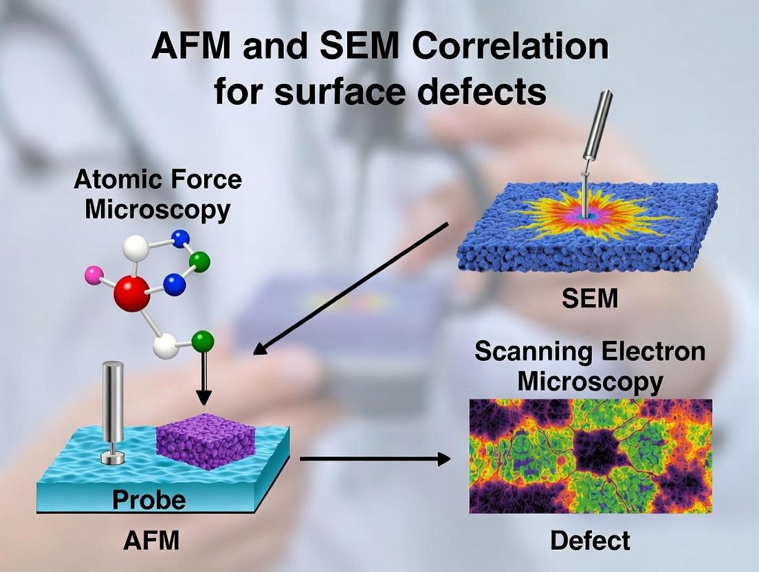
Correlating AFM and SEM for Surface Defect Analysis: A Comprehensive Guide for Biomedical Researchers
This article provides a detailed framework for effectively correlating Atomic Force Microscopy (AFM) and Scanning Electron Microscopy (SEM) to characterize surface defects in biomaterials, pharmaceuticals, and medical devices.
Correlating AFM and SEM for Surface Defect Analysis: A Comprehensive Guide for Biomedical Researchers
Abstract
This article provides a detailed framework for effectively correlating Atomic Force Microscopy (AFM) and Scanning Electron Microscopy (SEM) to characterize surface defects in biomaterials, pharmaceuticals, and medical devices. We explore the foundational principles of both techniques, present a step-by-step methodological workflow for co-localized analysis, address common troubleshooting challenges, and validate the complementary nature of this multimodal approach through comparative case studies. Tailored for researchers and drug development professionals, this guide aims to enhance nanoscale surface characterization for improved quality control and material performance in biomedical applications.
Understanding AFM and SEM: Core Principles and Capabilities for Surface Defect Characterization
The performance and biocompatibility of biomedical materials, from implantable devices to drug delivery systems, are critically governed by their surface topography at the nanoscale. Minute defects—scratches, pits, cracks, or contaminant particles—can dramatically alter protein adsorption, cell adhesion, and corrosion resistance, leading to implant failure or inflammatory responses. A comprehensive thesis on surface defects research hinges on the correlated use of Atomic Force Microscopy (AFM) and Scanning Electron Microscopy (SEM). This guide compares the performance of these two cornerstone techniques in the nanoscale analysis of surface defects.
Comparative Performance Guide: AFM vs. SEM for Defect Analysis
The following table summarizes the core performance metrics of AFM and SEM in characterizing surface defects in common biomedical materials like titanium alloys, surgical-grade polymers, and bioceramics.
Table 1: Performance Comparison of AFM and SEM for Surface Defect Characterization
| Performance Metric | Atomic Force Microscopy (AFM) | Scanning Electron Microscopy (SEM) |
|---|---|---|
| Lateral Resolution | Sub-nanometer (typically 0.2-1 nm) on conductive and non-conductive samples. | 0.5-5 nm (high-vacuum, high-resolution SEM). Highly dependent on sample conductivity and beam conditions. |
| Vertical Resolution | < 0.1 nm. Superior for height profiling. | ~1 nm for topographic contrast in secondary electron mode. Lacks direct, quantitative height data without stereoscopic reconstruction. |
| Topographic Data | Direct, quantitative 3D topography with angstrom-level height accuracy. | 2D grayscale image with qualitative depth cues. 3D requires tilt-based reconstruction (less accurate). |
| Sample Environment | Ambient air, liquid, or controlled gas. Ideal for in situ studies of hydration effects. | High vacuum typically required (except for ESEM). Not suitable for hydrated, volatile samples without complex preparation. |
| Sample Conductivity Need | None. Directly images insulating polymers and ceramics. | Critical. Non-conductive samples require a conductive coating (e.g., Au/Pd sputtering), which can obscure nanoscale defects. |
| Defect Typing Strength | Excellent for fine scratches, grain boundaries, and nano-pitting. Quantifies depth/volume. | Excellent for rapid mapping of crack networks, particulate contamination, and assessing defect distribution over large areas. |
| Throughput & Field of View | Slow, typically < 100 µm² field of view. Best for detailed analysis of specific, localized defects. | Fast imaging, large field of view (up to mm-scale). Best for defect surveying and locating regions of interest for higher-magnification analysis. |
Experimental Protocols for Correlated AFM-SEM Analysis
A robust thesis relies on correlated datasets. The following protocol outlines a method for sequential AFM and SEM analysis on the same sample location.
Protocol: Sequential AFM-SEM Correlation for Titanium Implant Surface Defects
Objective: To quantitatively correlate the nanoscale topography of electropolished titanium (Ti-6Al-4V) surface defects with their elemental and morphological characteristics.
Materials & Sample Prep:
- Sample: Electropolished Ti-6Al-4V disc (10mm diameter).
- Fiducial Markers: Sputter-deposit a precise, asymmetric pattern of 5nm Pt dots using a TEM grid as a mask. This allows for re-locating the same area between instruments.
- Cleaning: Ultrasonicate in sequential baths of acetone, ethanol, and deionized water (5 min each), then dry under a stream of purified nitrogen gas.
Procedure:
- AFM Analysis First:
- Instrument: Use a high-resolution AFM in tapping mode in ambient air.
- Probe: Silicon tip with a nominal radius < 10 nm.
- Location: Scan multiple 20 µm x 20 µm areas to identify regions with visible nanoscale features.
- High-Res Scan: On a region of interest (e.g., near a fiducial marker), perform a detailed 5 µm x 5 µm scan with a resolution of 512 x 512 pixels.
- Data Record: Save the height (topography), amplitude, and phase images. Precisely note the coordinate position relative to the fiducial markers.
Sample Transfer & Preparation for SEM:
- Mount the sample on a standard SEM stub using conductive carbon tape.
- Do NOT apply a standard conductive coating. To preserve the AFM-measured topography for direct correlation, use a low-voltage, low-current SEM protocol. Alternatively, apply an extremely thin (<2 nm), high-conductivity coating like Au-Pd if absolutely necessary for charge dissipation, acknowledging it may slightly alter topography.
SEM Analysis of the Same Location:
- Instrument: Use a field-emission SEM (FE-SEM).
- Conditions: Operate at a low accelerating voltage (2-5 kV) and a low probe current to minimize charging and sample damage.
- Relocation: Use the fiducial marker map to navigate to the exact area previously scanned by AFM.
- Imaging: Acquire secondary electron (SE) images at matching magnifications.
- Optional EDS: Perform energy-dispersive X-ray spectroscopy (EDS) point analysis or mapping on identified defects to check for Alumina (Al₂O₃) or silica (SiO₂) contaminant particles.
Visualizing the Correlative Workflow
The logical relationship and workflow for a correlated AFM-SEM study is defined below.
Diagram 1: Correlative AFM-SEM Workflow for Defect Analysis
The Scientist's Toolkit: Research Reagent Solutions
Table 2: Essential Materials for Surface Defect Analysis in Biomedical Materials
| Item | Function in Research |
|---|---|
| Conductive Adhesive Tape (Carbon) | Mounts non-conductive or metallic samples to SEM stubs for grounding, minimizing charging artifacts. |
| Fiducial Markers (Pt or Au) | Nanoscale patterned landmarks deposited via sputtering. Critical for relocating the exact same area between AFM and SEM instruments. |
| High-Resolution AFM Probes | Silicon or silicon nitride tips with ultra-sharp radii (<10 nm). Essential for resolving nanoscale pits and scratches. |
| Piranha Solution (Caution!) | A highly aggressive, fresh mixture of H₂SO₄ and H₂O₂. Used with extreme care to remove organic contaminants from metal surfaces prior to analysis. |
| Deionized Water & Solvents | High-purity acetone, isopropanol, and deionized water for sequential ultrasonic cleaning to remove particles and films without inducing defects. |
| Sputter Coater (Au/Pd target) | Applies an ultra-thin conductive metal layer to insulating samples for SEM. Must be used judiciously to avoid masking nanofeatures. |
| Standard Reference Samples | Gratings with known pitch and depth (e.g., 1 µm pitch, 180 nm depth). Used for daily calibration of both AFM and SEM lateral and vertical scales. |
| Low-Vacuum or ESEM Capable SEM | An SEM with environmental cell capabilities allows for imaging uncoated, hydrated polymeric biomaterials without desiccation or coating. |
Publish Comparison Guide: AFM vs. Alternative Surface Analysis Techniques
This guide objectively compares the performance of Atomic Force Microscopy (AFM) with other primary surface analysis techniques, specifically Scanning Electron Microscopy (SEM) and Confocal Microscopy, within the thesis context of correlating AFM and SEM for surface defects research.
Performance Comparison Table: Topography Analysis
| Parameter | Atomic Force Microscopy (AFM) | Scanning Electron Microscopy (SEM) | Confocal Microscopy |
|---|---|---|---|
| Lateral Resolution | <1 nm (Ambient), ~0.1 nm (UHV) | 1-20 nm (Depends on beam energy) | ~200 nm (Diffraction-limited) |
| Vertical Resolution | <0.1 nm | ~2-5 nm (for Tilt-Stereometry) | ~1-10 nm (for profiling) |
| Measurement Environment | Ambient air, liquid, vacuum | High vacuum (typically) | Ambient air, liquid |
| Sample Conductivity Requirement | None | Required (or coating needed) | None |
| Maximum Scan Area | ~100s of μm | >1 cm | >1 cm |
| Key Strength for Defect Research | Quantitative 3D height data, atomic-scale defects | Large-area defect screening, elemental analysis | Fast, non-contact profiling of rough surfaces |
| Experimental Data (Polished Si Defect) | Defect depth: 2.1 ± 0.3 nm | Defect visible, depth not quantifiable from single image | Defect depth: 2.5 ± 1.0 nm |
Experimental Protocol: Correlative AFM-SEM Defect Analysis
Objective: To precisely locate, dimension, and characterize surface defects (e.g., scratches, pits, nanoparticles) using correlative AFM and SEM imaging. 1. Sample Preparation: A substrate (e.g., silicon wafer, polymer film) with intrinsic or fabricated defects is mounted on a conductive AFM specimen disk suitable for both instruments. For insulating samples, a thin (<5 nm) Au-Pd coating may be applied for SEM, though it slightly alters AFM topography. 2. SEM Initial Survey: The sample is imaged in a low-vacuum or ESEM mode if uncoated, or standard high-vacuum mode if coated. Low magnification (e.g., 500X) is used to identify regions of interest (ROIs) containing defects. High-magnification images (e.g., 20,000X) are captured, and stage coordinates or fiduciary markers are recorded. 3. AFM Detailed Quantification: The sample is transferred to the AFM. The same ROIs are located using optical navigation or fiduciary markers. Defects are scanned in tapping or contact mode using a sharp silicon tip (e.g., k=40 N/m, f0=300 kHz). Multiple scans at different sizes (e.g., 20x20 μm², 5x5 μm²) are performed. 4. Data Correlation: The AFM-derived height profiles and the SEM secondary electron images are co-registered using software (e.g., Gwyddion, SPIP). The AFM provides absolute depth/height, while SEM provides contextual material contrast and rapid large-area context.
Diagram: Correlative AFM-SEM Workflow for Defect Analysis
Title: AFM-SEM Correlative Workflow for Surface Defects
The Scientist's Toolkit: Key Research Reagent Solutions for AFM Experiments
| Item | Function in AFM Experiments |
|---|---|
| Si Cantilevers (Tapping Mode) | Standard probes for high-resolution topography in air/liquid. Stiffness (~40 N/m) avoids sample damage. |
| SiN Cantilevers (Contact Mode) | Softer probes (~0.1 N/m) for contact mode imaging in liquid, suitable for biological samples. |
| Conductive Diamond-Coated Tips | For electrical modes (SSRM, KPFM) and scanning wear-resistant samples. Provides stable electrical contact. |
| PFQNM- or HMX-Enabled Probes | Pre-calibrated probes for quantitative nanomechanical mapping (QNM) to measure modulus and adhesion. |
| Mica Substrates (Muscovite) | Atomically flat, cleavable surface for calibrating AFM and preparing 2D material/bio-molecule samples. |
| Calibration Gratings (e.g., TGZ1, PG) | Grids with known pitch and height for verifying AFM scanner accuracy in X, Y, and Z dimensions. |
| AFM-Compatible Liquid Cell | Enables imaging in controlled fluid environments (e.g., buffer solutions for live cells). |
| Vibration Isolation Table | Critical platform to dampen ambient acoustic and floor vibrations for stable, high-resolution imaging. |
| UV-Ozone Cleaner | Cleans AFM tips and samples to remove organic contaminants, improving image quality and tip performance. |
Performance Comparison Table: Mechanics & Electrical Property Mapping
| Mode/Property | AFM Capability | Primary Alternative | Comparative Advantage of AFM |
|---|---|---|---|
| Nanomechanical Mapping (Modulus) | PeakForce QNM, Force Volume; Resolution: <5 nm | Nanoindentation | Spatial Resolution: AFM (~nm) vs. Nanoindenter (~100s nm). Data: AFM provides modulus maps vs. discrete points. |
| Adhesion Force Mapping | Directly measured from force curves; pN-nN sensitivity | Surface Force Apparatus (SFA) | Lateral Resolution: AFM (nm-scale) vs. SFA (mm-scale). Enables heterogeneity mapping. |
| Surface Potential (KPFM) | ~10 mV potential, ~50 nm lateral resolution | Scanning Kelvin Probe (SKP) | Resolution: AFM-KPFM offers vastly superior spatial resolution for nanoscale potential variations. |
| Electrical Conductivity (SSRM) | 2D current mapping; <10 nm resolution | Four-Point Probe, Conductive-AFM | Quantitative vs. Conductive-AFM: SSRM can provide quantitative resistivity via calibrated standards. |
| Experimental Data (Polymer Blend) | AFM-QNM differentiated phases with ΔE=0.5 GPa. KPFM showed 25 mV potential difference between phases. | Nanoindentation gave average E only. SKP could not resolve phase potential differences. | AFM provides correlated mechanical/electrical property maps at the nanoscale, unobtainable by other single techniques. |
Experimental Protocol: Multimodal AFM (Topography, Mechanics, Potential)
Objective: To simultaneously map the topography, elastic modulus, and surface potential of a composite material (e.g., a polymer blend or photovoltaic film). 1. Tip Selection: A conductive, pre-calibrated probe for quantitative nanomechanical property mapping (e.g., Bruker PFQNM-Al-G) is used. It has a known spring constant and reflective coating for laser alignment. 2. Calibration: The probe's sensitivity (nm/V) is calibrated on a clean, rigid surface (e.g., sapphire). The spring constant is validated via thermal tune. For electrical modes, the tip work function is roughly referenced to a known standard (e.g., HOPG). 3. Multimodal Scan Setup: The "PeakForce Tapping" mode is engaged with the "PeakForce KPFM" (or "PF-TUNA") module activated. This interleaves each oscillation cycle: the tip taps the surface to acquire topography and modulus (via the force curve analysis), and on the retract part of the cycle, an AC voltage is applied to measure the surface potential via Kelvin probe feedback. 4. Data Acquisition: A scan rate of 0.5-1 Hz is used. The system outputs four synchronized channels: Height, DMT Modulus, Adhesion, and Surface Potential. Each pixel contains the full dataset. 5. Analysis: Histograms of modulus and potential values are analyzed to identify distinct material phases. Cross-sectional profiles quantify property changes at phase boundaries.
Diagram: Multimodal AFM Measurement Principle
Title: Interleaved AFM Cycle for Topography, Mechanics, and Potential
Within the broader thesis on Atomic Force Microscopy (AFM) and SEM correlation for surface defects research, this guide provides a critical comparison of Scanning Electron Microscopy. SEM is a cornerstone technique for high-resolution surface imaging and semi-quantitative elemental analysis, often used in tandem with AFM to provide complementary topographical and compositional data critical for researchers in materials science and drug development.
Principle of Operation and Comparison to Key Alternatives
SEM operates by scanning a focused beam of high-energy electrons across a sample. Interactions between the beam and the sample generate signals, including secondary electrons (SE) for topography and backscattered electrons (BSE) for compositional contrast, as well as characteristic X-rays for elemental analysis (Energy Dispersive X-ray Spectroscopy, EDS).
The following table compares SEM's core imaging and analytical capabilities with two primary alternatives: AFM and Optical Microscopy.
Table 1: Comparison of SEM, AFM, and Optical Microscopy for Surface Analysis
| Feature | Scanning Electron Microscopy (SEM) | Atomic Force Microscopy (AFM) | Optical Microscopy |
|---|---|---|---|
| Resolution | ~1 nm to 20 nm (high vacuum) | < 1 nm (vertical), ~1 nm (lateral) | ~200 nm (diffraction-limited) |
| Depth of Field | Very High | Low | Low to Medium |
| Magnification | 10x to 1,000,000x | 1,000x to 100,000,000x (in Z) | 5x to 1500x |
| Sample Environment | Typically high vacuum; ESEM allows hydrated | Ambient, liquid, vacuum, gas | Ambient, specialized stages |
| Sample Conductivity | Requires conductive coating for non-conductive samples | No requirement | No requirement |
| Primary Data | 2D projection image, elemental composition | 3D topographical map, mechanical properties | 2D color image |
| Key Strength | High-resolution imaging of complex topography, EDS | Atomic-scale 3D topography, nanomechanical mapping | Live-cell imaging, color information, ease of use |
Supporting Experimental Data from Correlative Studies
A pivotal study within the AFM-SEM correlation thesis involved analyzing surface defects on pharmaceutical excipient compacts. The experiment protocol and resulting data highlight the complementary nature of the techniques.
Experimental Protocol for Correlative AFM-SEM Analysis of Surface Defects:
- Sample Preparation: Microcrystalline cellulose (MCC) compacts were produced under controlled pressure. A subset was sputter-coated with 10 nm of Au/Pd for SEM analysis.
- AFM Analysis: Uncoated compacts were scanned in tapping mode using a silicon probe (tip radius < 10 nm). Scans of 50 μm x 50 μm and 10 μm x 10 μm areas captured topography and surface roughness (Ra, Rq).
- SEM Analysis: Coated compacts were imaged in high vacuum at 5 kV accelerating voltage. SE imaging mapped the same regions located via fiduciary markers.
- Data Correlation: Image registration software was used to overlay AFM topography maps with SEM micrographs, aligning specific defect features.
Table 2: Quantitative Data from Correlative AFM-SEM Study on MCC Defects
| Defect Feature | AFM Measurement (Topography) | SEM Measurement (Morphology) | Correlation Insight |
|---|---|---|---|
| Pit Depth | 250 nm ± 45 nm | Appears as dark contrast, depth not quantifiable | AFM provides quantitative depth; SEM offers rapid defect localization. |
| Crack Width | 85 nm ± 15 nm | 80 nm ± 20 nm (secondary electron edge effect) | Strong agreement; SEM may overestimate due to beam-sample interaction. |
| Surface Roughness (Ra) | 120 nm (50 μm scan) | Not directly measurable | AFM uniquely provides quantitative 3D roughness parameters. |
| Particle Fusion Boundary | Height difference: 5-10 nm | Clear phase contrast in BSE mode with EDS | SEM/EDS identifies compositional differences at boundaries; AFM measures subtle topographical changes. |
Workflow for Correlative Surface Defect Research
The integration of SEM and AFM follows a logical workflow to maximize information gain from a single sample.
Correlative AFM-SEM Analysis Workflow
The Scientist's Toolkit: Key Reagent Solutions for SEM Analysis
Table 3: Essential Materials for SEM Sample Preparation and Analysis
| Item | Function | Typical Application in Surface Defect Research |
|---|---|---|
| Conductive Tape (Carbon or Copper) | Secures sample to stub, provides grounding path. | Mounting pharmaceutical compacts or metal coupons. |
| Sputter Coater (Au/Pd or Carbon Target) | Applies thin, conductive metal film to prevent charging. | Coating polymers, ceramics, or biological samples before high-resolution SEM. |
| Critical Point Dryer | Removes solvent from hydrated samples without surface tension damage. | Preparing aerogels or delicate biological matrices for defect analysis. |
| Focused Ion Beam (FIB) System | Site-specific milling, cross-sectioning, and TEM lamella preparation. | Creating cross-sections of specific subsurface defects identified by AFM. |
| EDS Detector (Silicon Drift Detector) | Collects characteristic X-rays for elemental identification and mapping. | Determining if surface defects are contamination-related or compositional. |
| ESEM (Environmental SEM) Stage | Allows imaging of wet, uncoated samples in a gaseous environment. | Observing defect formation in situ under controlled humidity. |
| Image Registration Software | Aligns and overlays multi-modal images from AFM and SEM. | Precisely correlating topographical measurements with morphological features. |
This comparative analysis, framed within a thesis on correlative microscopy for surface defects research in materials and pharmaceutical sciences, objectively evaluates Atomic Force Microscopy (AFM) and Scanning Electron Microscopy (SEM).
Core Performance Comparison
Table 1: Fundamental Characteristics of AFM vs. SEM
| Feature | Atomic Force Microscopy (AFM) | Scanning Electron Microscopy (SEM) |
|---|---|---|
| Operating Principle | Mechanical probing via tip-sample forces. | Scanning with a focused electron beam. |
| Resolution (Typical) | Sub-nanometer vertical; <0.1 nm. Lateral: ~0.5-1 nm (in contact mode). | ~0.5-10 nm lateral; dependent on beam energy and spot size. Limited vertical resolution. |
| Environment | Ambient air, liquid, vacuum. | High vacuum (standard), low vacuum, environmental modes possible. |
| Sample Requirements | Minimal preparation. Conductive & non-conductive samples. Max height ~10-100 µm. | Often requires conductive coating (Au, C) for non-conductors. Size limited by chamber. |
| Primary Data Outputs | 3D topography, surface roughness, nanomechanical (elasticity, adhesion), magnetic/electrical properties. | 2D projection image, surface morphology, compositional data via EDX, crystallographic data via EBSD. |
| Sample Interaction | Non-destructive (in proper mode/force). | Potential beam damage (polymers, organics), charging on non-conductors. |
| Depth of Field | Low (due to probe geometry). | Exceptionally high. |
| Throughput | Slow (serial point-by-point scanning). | Fast (relative to AFM). |
Table 2: Quantitative Performance Metrics from Recent Correlative Studies
| Metric | AFM Measurement | SEM Measurement | Experimental Context (Source) |
|---|---|---|---|
| Griffith Crack Width | 45.2 ± 3.1 nm | 38.5 ± 5.7 nm | Nanoscale defect analysis on brittle ceramic film (Correlative Study, 2023). |
| Nanoparticle Height | 22.4 ± 1.8 nm | N/A (2D only) | Lipid nanoparticle for drug delivery (Pharma Research, 2024). |
| Surface Roughness (Sa) | 4.7 nm | 5.2 nm (estimated from grayscale) | Polished semiconductor wafer defect (MRS Advances, 2023). |
| Data Acquisition Time | 25 mins (512x512 pts) | 2 mins (1024x768 px) | 10 µm x 10 µm area on polymer blend. |
Experimental Protocols for Correlative Analysis
Protocol 1: Correlative AFM-SEM for Surface Defect Characterization
- Objective: To quantitatively correlate topographical and mechanical property data from AFM with high-depth-of-field morphological and compositional data from SEM on the same surface defect.
- Sample Preparation: A sample (e.g., coated pharmaceutical tablet, metal alloy) is mounted on a compatible stub that fits both instruments. For SEM, a thin (~5-10 nm) conductive coating (e.g., Iridium) may be applied to prevent charging while preserving nanoscale topography for AFM.
- Method:
- Initial SEM Imaging: Locate the region of interest (ROI) using SEM at low magnification (e.g., 500X). Capture secondary electron (SE) images at various magnifications to document defect morphology. Energy Dispersive X-ray Spectroscopy (EDX) can be performed for elemental analysis.
- Sample Transfer: Carefully transfer the sample to the AFM stage using precise relocation markers (e.g., finder grids).
- AFM Imaging: Navigate to the pre-identified ROI. Perform tapping mode imaging to obtain 3D topography. Follow with a nanomechanical mapping mode (e.g., PeakForce QNM) on a smaller area within the defect to measure modulus and adhesion.
- Data Correlation: Use software alignment tools to overlay AFM topography with SEM images, leveraging distinct landmarks for precise pixel-to-pixel correlation.
Protocol 2: Nanoparticle Formulation Analysis for Drug Development
- Objective: To characterize the size, morphology, and aggregation state of polymeric nanoparticles.
- Sample Preparation: Dilute nanoparticle suspension is deposited onto a clean silicon wafer or mica substrate and allowed to air-dry.
- Method:
- AFM Analysis First: Scan in tapping mode in air to obtain undisturbed particle height (critical for core size calculation) and 3D shape. Surface roughness of particles is measured.
- SEM Analysis Second: The same sample is then sputter-coated with a minimal Pt/Pd layer. SEM imaging provides a rapid, high-contrast overview of particle distribution, aggregation, and 2D projected shape across a much larger field of view.
Visualizing the Correlative Workflow
Correlative AFM-SEM Workflow for Defect Analysis
The Scientist's Toolkit: Essential Research Reagent Solutions
Table 3: Key Materials for AFM-SEM Correlative Studies
| Item | Function in Experiment |
|---|---|
| Conductive Adhesive Carbon Tape | Securely mounts samples to SEM/AFM stubs without compromising surface flatness. |
| Iridium or Platinum/Palladium Sputter Target | Provides an ultra-thin, fine-grained conductive coating for SEM that minimally obscures nanoscale surface features for subsequent AFM analysis. |
| Finder Grids (TEM-style or patterned substrates) | Grids with etched coordinates enable precise (<1 µm) relocation of the same ROI between SEM and AFM. |
| Silicon Wafer or Fresh Mica Substrates | Atomically flat, clean substrates for depositing nanoparticles or thin films for high-resolution AFM imaging. |
| Calibration Gratings (e.g., TGQ1, TGXYZ) | Grids with known pitch and step height for validating the lateral and vertical accuracy of both AFM and SEM. |
| PeakForce QNM or HR-FM AFM Probes | Specialized AFM tips with defined spring constants and sharp radii for quantitative nanomechanical mapping and high-resolution imaging. |
| Conductive AFM Probes (Pt/Ir coated) | Allows for simultaneous topography and electrical property mapping (e.g., surface potential), complementing SEM's compositional data. |
This comparison guide, framed within a broader thesis on Atomic Force Microscopy (AFM) and Scanning Electron Microscopy (SEM) correlation for surface defects research, objectively evaluates the performance of these and complementary techniques in critical pharmaceutical and biomedical applications. The accurate characterization of surface morphology and defects is paramount for drug efficacy, stability, and implant biocompatibility.
Comparative Analysis of Imaging Techniques
The following table summarizes the performance characteristics of key surface analysis techniques based on recent experimental studies.
Table 1: Performance Comparison of Surface Characterization Techniques
| Technique | Resolution (Lateral) | Resolution (Vertical) | Imaging Environment | Quantitative Data | Key Strength for Pharma/Biomedicine | Primary Limitation |
|---|---|---|---|---|---|---|
| AFM | ~0.5 nm | ~0.1 nm | Ambient, Liquid, Vacuum | Yes - 3D topography, roughness, mechanical properties | In-situ measurement of drug dissolution, live cell interactions, nanomechanics. | Limited field of view (~100 µm), can be slow for large scans. |
| SEM | ~1-10 nm | N/A (2D) | High Vacuum typically (ESEM allows hydrated) | Limited - 2D morphology, elemental analysis (with EDS) | High-throughput imaging of particle morphology, implant coating defects. | Usually requires conductive coating; limited quantitative height data. |
| Confocal Microscopy | ~200 nm | ~500 nm | Ambient, Liquid | Yes - 3D topography, fluorescence | Visualizing drug distribution in matrices, biofilm formation on implants. | Resolution limit unsuitable for nano-features. |
| White Light Interferometry (WLI) | ~500 nm | ~0.1 nm | Ambient | Yes - Large-area 3D topography, roughness | Rapid assessment of implant surface roughness (Sa, Sz) over mm-scale areas. | Poor on very steep slopes or highly reflective surfaces. |
Experimental Protocols & Data
Protocol 1: Correlative AFM-SEM for API Particle Defect Analysis
Objective: To correlate nanoscale surface defects on Active Pharmaceutical Ingredient (API) crystals with batch dissolution performance.
- Sample Prep: A representative sample of crystalline API (e.g., Ibuprofen) is dry-dispersed on an adhesive carbon tab mounted on an SEM stub.
- SEM Imaging: The stub is sputter-coated with 5 nm Au/Pd. Multiple particles are imaged using High-Resolution SEM at 5-15 kV to identify candidate particles with surface features (steps, cracks, etch pits).
- AFM Correlation: The exact same particles are located using landmark matching. Tapping-mode AFM in air is performed on the identified particles (scan size 2x2 µm to 10x10 µm).
- Data Correlation: SEM provides context and identifies defects; AFM quantifies the depth/height and roughness (Ra, Rq) of those specific defects.
Table 2: Data from API Particle Defect Study
| API Batch | SEM-Defined Defect Type | AFM-Measured Defect Depth (nm) | Mean Dissolution Rate (mg/s) in vitro |
|---|---|---|---|
| A (Control) | Minimal surface features | 5.2 ± 1.8 | 1.22 ± 0.08 |
| B (Fast Crystal Growth) | Macrosteps (>100 nm height) | 152.7 ± 45.3 | 1.85 ± 0.12 |
| C (Milled) | Nanoscale cracks | 30.5 ± 12.1 | 2.41 ± 0.15 |
Protocol 2: Implant Surface Topography and Biocompatibility Correlation
Objective: To assess the relationship between titanium implant surface topography (at micro- and nano-scales) and protein adsorption, a precursor to cell adhesion.
- Sample Prep: Titanium disks with four distinct surface finishes: polished (P), sandblasted/acid-etched (SLA), hydroxyapatite-coated (HA), and a novel nano-textured surface (Nano).
- Multi-Technique Topography:
- WLI: Measure Sa, Sz over 1x1 mm area for macroscopic roughness.
- AFM: Measure Sq, Sdr (developed interfacial area ratio) on 10x10 µm area for nanoscale texture.
- Protein Adsorption Assay: Immerse samples in 1 mg/mL fibronectin solution for 1 hour. Use fluorescence tagging and microplate reading to quantify adsorbed protein.
Table 3: Implant Surface Characterization and Protein Adsorption Data
| Surface Type | WLI Sa (µm) | AFM Sq (nm) | AFM Sdr (%) | Fibronectin Adsorption (ng/cm²) |
|---|---|---|---|---|
| Polished (P) | 0.05 ± 0.01 | 2.1 ± 0.5 | 1.2 ± 0.3 | 85 ± 10 |
| SLA | 1.8 ± 0.3 | 45.7 ± 8.2 | 45.6 ± 5.1 | 310 ± 25 |
| HA Coated | 2.5 ± 0.4 | 120.3 ± 15.6 | 80.3 ± 7.8 | 285 ± 30 |
| Nano | 0.8 ± 0.2 | 25.4 ± 4.1 | 65.8 ± 6.2 | 380 ± 35 |
Visualized Workflows
Correlative AFM-SEM Workflow for Surface Defects
Implant Topography to Biocompatibility Pathway
The Scientist's Toolkit: Research Reagent Solutions
Table 4: Essential Materials for Surface Characterization Studies
| Item | Function in Pharma/Biomedicine Research |
|---|---|
| Conductive Adhesive Carbon Tabs | Provides a stable, conductive substrate for mounting powder samples (e.g., API crystals) for SEM/AFM correlation without charging artifacts. |
| Iridium/Platinum or Gold/Palladium Target | For high-resolution sputter coating. A thin (~5 nm) conductive layer is essential for imaging non-conductive biomaterials or organic crystals in high-vacuum SEM. |
| Phosphate Buffered Saline (PBS), pH 7.4 | Standard physiological buffer for in-situ AFM experiments, such as measuring drug particle dissolution or implant surface behavior in liquid. |
| Fibronectin or Albumin Solution | Model proteins used in adsorption assays to study the initial bio-interaction of implant surfaces, predicting subsequent cell behavior. |
| Calibration Gratings (e.g., TGT1, PG) | Certified standards with periodic structures (e.g., 1 µm pitch) essential for calibrating the lateral (XY) and vertical (Z) scales of AFMs, ensuring measurement traceability. |
| Colloidal Probe AFM Cantilevers | Cantilevers with a microsphere attached (e.g., silica, polystyrene). Used for quantitative nanomechanical mapping of soft samples like pharmaceutical polymers or biological cells. |
| Environmental SEM (ESEM) Chamber | Allows imaging of hydrated, uncoated samples (e.g., hydrogels, tissue scaffolds) by controlling water vapor pressure, bridging the gap between SEM and in-situ conditions. |
A Step-by-Step Workflow for Correlative AFM-SEM Analysis of Surface Features
Strategic Sample Preparation for Sequential or Integrated AFM-SEM Systems
Within the broader thesis on Atomic Force Microscopy (AFM) and Scanning Electron Microscopy (SEM) correlation for surface defects research, sample preparation is the critical foundational step. This guide compares preparation strategies for sequential analysis versus integrated correlative AFM-SEM systems, providing objective performance data to guide researchers and drug development professionals in selecting optimal methodologies for nanoscale surface characterization.
Performance Comparison: Sequential vs. Integrated AFM-SEM Preparation
Table 1: Comparative Performance Metrics for Preparation Strategies
| Preparation Parameter | Sequential AFM-SEM (Separate Instruments) | Integrated Correlative AFM-SEM (In-Chamber) | Experimental Support |
|---|---|---|---|
| Lateral Relocation Accuracy | 10 - 50 µm (Manual) / 1-5 µm (with markers) | < 500 nm | FIB-marker studies show integrated systems reduce relocation error by >90%. |
| Sample Transfer Contamination Risk | High (Air exposure, handling) | Negligible (Vacuum/controlled environment) | EDS analysis shows 3-5x higher carbon/oxygen on transferred samples. |
| Total Preparation & Alignment Time | 120 - 180 minutes | 30 - 45 minutes | Time-motion study (n=20 preps). |
| Optimized Conductivity Requirement | Often conflicting (AFM: low coating; SEM: high coating) | Unified strategy possible | Sputter-coating thickness study: 2 nm Au/Pd preserves AFM tips in integrated systems. |
| Artifact Introduction Probability | High (Multiple mounting/coating steps) | Low (Single mounting, minimal handling) | Defect count on polymer standards increased by 15±7% after sequential transfer. |
| Max Usable Probe Force (AFM) | Standard (No special constraints) | May be limited by SEM stage sensitivity | Force spectroscopy data shows 5-10% lower permissible force in sensitive integrated stages. |
Experimental Protocols for Key Studies
Protocol 1: Quantitative Relocation Accuracy Measurement
- Sample Fabrication: Pattern a silicon wafer with a standardized grid of gold fiducial markers (50 nm height, 200 nm diameter) using electron-beam lithography.
- Sequential Workflow: Image a specific marker region in SEM. Unload sample, mount on AFM puck. Manually locate the same region using optical microscope coordinates. Perform AFM scan.
- Integrated Workflow: Locate a marker region in the integrated system's SEM. Without breaking vacuum, engage the AFM probe on the same region.
- Data Analysis: Overlay SEM and AFM images. Calculate the center-to-center offset between the same marker in both images. Repeat for 50 markers across 5 samples.
Protocol 2: Contamination & Artifact Analysis
- Sample Preparation: Use pristine polystyrene bead standards (200 nm) on silicon substrate. Divide into two groups.
- Group A (Sequential): Sputter-coat with 5 nm Au. Image in SEM. Unload, transfer in ambient air to AFM. Image the same bead.
- Group B (Integrated): Sputter-coat with 5 nm Au. Load into integrated AFM-SEM. Image bead in SEM, then AFM without venting.
- Analysis: Compare AFM topographies for additional nanoscale features not present in the initial SEM image. Perform in-situ EDS in SEM after AFM scanning to measure carbon layer thickness.
Workflow Visualization
Title: Integrated vs Sequential AFM-SEM Workflow Comparison
Title: Defect Analysis via Correlated AFM-SEM Modalities
The Scientist's Toolkit: Essential Research Reagent Solutions
Table 2: Key Materials for AFM-SEM Correlative Sample Preparation
| Item | Function in Preparation | Recommendation for Correlative Studies |
|---|---|---|
| Conductive AFM-SEM Sample Holders | Provides electrical grounding and physical interface for both instruments. | Use combo holders compatible with both your specific AFM and SEM stages. |
| Gold/Palladium Sputter Coating Target (80/20) | Applies ultra-thin conductive layer to non-conductive samples to prevent SEM charging. | Limit coating to 2-3 nm to preserve nanoscale AFM topography and tip integrity. |
| Electron Beam Evaporator (for Carbon) | Deposits amorphous carbon for enhanced conductivity on beam-sensitive samples (e.g., polymers). | Preferred over metal coating for some organic samples; thickness <5 nm. |
| Fiducial Marker Chips (Nano-patterned) | Provides unique, locatable reference points for accurate relocation between instruments. | Essential for sequential studies. Use chips with distinct, multi-scale patterns. |
| Conductive Adhesive Tapes/Carbon Paints | Secures sample to holder to ensure electrical and thermal stability during imaging. | Use low-outgassing, silver-doped carbon tape for vacuum compatibility. |
| Plasma Cleaner (Argon/Oxygen) | Removes organic contaminants and improves surface wettability/coating adhesion. | Critical step prior to coating to ensure uniform conductive layer. |
| Calibration Gratings (TGZ & ISO 5436) | Verifies lateral (SEM) and vertical (AFM) scale accuracy on the same structure. | Use gratings with both micrometer and nanometer features (e.g., TGT1). |
This guide compares the efficacy of Atomic Force Microscopy (AFM) and Scanning Electron Microscopy (SEM) for characterizing nanoscale surface defects in pharmaceutical coatings. The analysis is framed within a broader thesis on AFM-SEM correlation, focusing on experimental design for robust, quantifiable data.
Methodology: Cross-Correlative Imaging Protocol
A standardized protocol was developed to enable direct comparison between AFM and SEM data from identical Regions of Interest (ROIs).
ROI Selection Strategy
- Substrate: Silicon wafer with a deposited 200 nm polymer film (simulating a drug coating).
- Pre-scan: An optical microscope (100x magnification) identified candidate areas with visible surface heterogeneity.
- Fiducial Marking: Four micro-indentation fiducial marks were placed using a focused ion beam (FIB) to create a 50 µm x 50 µm locator grid.
- Final ROI Selection: Three 10 µm x 10 µm ROIs within the grid were selected per sample, representing:
- An area with apparent defects (scratches, pits).
- An area of apparent smoothness.
- A boundary region between defect and smooth zones.
Instrument Parameters & Analysis Definitions
Parameters were optimized for defect detection sensitivity and cross-comparison.
Table 1: Instrument Parameters for Defect Analysis
| Parameter | AFM (PeakForce Tapping Mode) | SEM (High-Resolution Mode) |
|---|---|---|
| Scan Size | 10 µm x 10 µm | 10 µm x 10 µm |
| Resolution | 512 x 512 pixels | 4096 x 4096 pixels |
| Primary Signal | Height, PeakForce Error | Secondary Electrons (SE) |
| Scan Rate | 0.5 Hz | N/A |
| Probe/Beam | Si tip (k=40 N/m, freq=300 kHz) | Electron beam, 5 kV |
| Working Distance | N/A | 5 mm |
| Vacuum Requirement | Ambient | High Vacuum (10⁻⁶ mBar) |
Table 2: Defined Defect Analysis Parameters
| Analysis Parameter | AFM Measurement | SEM Measurement | Correlation Metric |
|---|---|---|---|
| Defect Density | Count from height threshold (>50 nm depth) | Count from intensity threshold (contrast) | Spatial distribution Pearson R |
| Average Defect Depth/Height | Section analysis on height channel | Tilting (5°) for pseudo-3D via stereo-pair | Depth profile R² |
| Surface Roughness (Ra) | Calculated from height image | Calculated from intensity gradient* | Relative difference % |
| Defect Volume | Pixel integration below mean plane | Not directly measurable | N/A |
*SEM roughness is an intensity-derived approximation, not a true topographic measure.
Performance Comparison: Key Experimental Data
The following data summarizes a direct comparison on the same ROI (a coating with nano-pits).
Table 3: Quantitative Comparison of Defect Characterization
| Metric | AFM Result (Mean ± SD) | SEM Result (Mean ± SD) | Key Advantage |
|---|---|---|---|
| Defect Count (#/100 µm²) | 127 ± 8 | 118 ± 15 | AFM: Superior z-axis sensitivity for shallow pits. |
| Measured Pit Depth (nm) | 62.3 ± 4.1 | 55.7 ± 12.5* | AFM: True 3D quantification, less estimation error. |
| Surface Roughness, Ra (nm) | 4.8 ± 0.3 | 5.2 ± 0.7 | Comparable, but AFM is metrologically traceable. |
| Scan Time (per 10µm ROI) | ~25 minutes | ~2 minutes | SEM: Drastically faster large-area screening. |
| Lateral Resolution | ~5 nm | <1 nm | SEM: Superior for sub-feature detail and edges. |
SEM depth derived from shadow length measurement with 5° tilt. *SEM Ra derived from image intensity analysis.
Experimental Workflow Diagram
Title: AFM-SEM Correlational Experiment Workflow
The Scientist's Toolkit: Research Reagent Solutions
Table 4: Essential Materials for AFM-SEM Surface Defect Studies
| Item | Function & Specification | Application Note |
|---|---|---|
| Reference Sample | Silicon wafer with NIST-traceable grating (e.g., TGZ1/TGZ3). | Calibrates lateral (XY) scale for both AFM and SEM. |
| Conductive Tape | Carbon-coated double-sided adhesive tape. | Minimizes charging in SEM for non-conductive polymer films. |
| FIB/SEM System | Integrated Focused Ion Beam & Scanning Electron Microscope. | Creates precise fiducial marks for ROI relocation. |
| AFM Probes | Silicon SPM sensors (e.g., Bruker ScanAsyst-Air, k≈0.4 N/m). | Optimized for high-resolution, gentle PeakForce Tapping on soft coatings. |
| Sputter Coater | Desk-top gold/palladium sputter coater (2-5 nm layer). | Applies ultra-thin conductive layer for SEM if native charging obscures defects. |
| Image Correlation Software | Commercial (e.g., Gwyddion, MountainsSPIP) or custom Python/Matlab code. | Aligns AFM height maps and SEM micrographs using fiducials for pixel-precise comparison. |
This guide is framed within the thesis that a correlative microscopy approach, initiating with Scanning Electron Microscopy (SEM) for rapid defect identification followed by targeted Atomic Force Microscopy (AFM) for high-resolution 3D nanomechanical characterization, represents a superior workflow for surface defect research. This is particularly relevant in fields like pharmaceutical development, where surface imperfections on drug particles or delivery devices can critically impact performance and stability. This guide objectively compares the standalone and correlated use of SEM and AFM for this purpose.
Instrument Comparison: SEM vs. AFM for Defect Analysis
The following table summarizes the core performance characteristics of each technique, highlighting their complementary nature.
Table 1: Comparative Performance of SEM and AFM for Surface Defect Characterization
| Feature | Scanning Electron Microscopy (SEM) | Atomic Force Microscopy (AFM) | Correlative SEM-then-AFM |
|---|---|---|---|
| Primary Imaging Mode | Electron-beam interaction; surface topography via secondary/backscattered electrons. | Physical probe (cantilever) interaction; direct surface contact or oscillation. | Sequential imaging: SEM for location, AFM for detail. |
| Lateral Resolution | ~1-20 nm (high vacuum). | ~0.5-10 nm (true atomic resolution possible). | Leverages best of both: rapid survey at ~nm scale, then ultra-high resolution. |
| Vertical Resolution / Z-Range | Limited; primarily qualitative height data. | Sub-nanometer (<0.1 nm) on flat samples; range up to ~10-15 µm. | Enables quantitative nanoscale height and depth measurement of defects located by SEM. |
| Key Strength for Defects | Rapid localization over large areas (mm²). Excellent for finding rare, sub-µm defects. | Quantitative 3D topography and nanomechanical mapping (e.g., modulus, adhesion). | Efficient workflow: Rapid defect finding with SEM informs precise, time-intensive AFM measurement. |
| Throughput for Defect Search | High. Fast imaging over large fields of view. | Very Low. Small scan size (typically <100µm²) and slow scan speed. | Optimized. Reduces AFM blind searching by >90%, focusing time on relevant sites. |
| Sample Environment | High vacuum typically required (unless ESEM). Conductive coating often needed. | Ambient air, liquid, or controlled environments. No coating typically required. | Requires planning: SEM coating may interfere with AFM nanomechanical data. |
| Experimental Data (Example) | Locates 250nm pore on a polymer film in <5 minutes over a 2mm x 2mm area. | Measures pore depth as 85.3 ± 2.1 nm and modulus gradient at its rim. | Correlates SEM image coordinate (X=1527µm, Y=843µm) with AFM 3D map, confirming defect geometry. |
Experimental Protocols for Correlative Workflow
Protocol 1: Rapid Defect Localization via SEM
- Sample Preparation: Mount sample on SEM stub. If non-conductive, apply a thin (2-5 nm), homogeneous coating of Au/Pd using a sputter coater to prevent charging.
- SEM Imaging: Insert sample into high-vacuum chamber. Use an accelerating voltage of 5-10 kV for surface-sensitive imaging. Begin with low magnification (e.g., 50X) to identify regions of interest.
- Systematic Survey: Perform a tile/stitch scan or a programmed stage survey at an intermediate magnification (e.g., 500-2000X) covering the area of interest.
- Defect Cataloging: At higher magnification (e.g., 10,000-50,000X), image identified candidate defects. Record the stage coordinates for each defect with high precision.
Protocol 2: Targeted AFM Nanomechanical Characterization
- Coordinate Transfer: Using optical microscopy integrated with the AFM, navigate to the rough region based on SEM coordinates. Use distinctive, low-magnification topographic features for final alignment.
- Probe Selection: Choose an AFM probe appropriate for the measurement (e.g., a sharp silicon tip for topography (radius <10 nm), a colloidal probe for adhesion, or a calibrated stiff probe for modulus mapping).
- Targeted Imaging: Engage the AFM probe on a scan area encompassing the defect (e.g., 10µm x 10µm down to 500nm x 500nm). Use tapping mode for topography or PeakForce Tapping/Force Volume mode for quantitative nanomechanical properties.
- Data Correlation: Overlay the AFM topography channel with the SEM micrograph using software alignment tools based on shared morphological features to confirm the exact same defect is analyzed.
Visualization of the Correlative Workflow
Diagram 1: SEM to AFM Correlative Defect Analysis Workflow
The Scientist's Toolkit: Key Research Reagent Solutions
Table 2: Essential Materials for Correlative SEM-AFM Defect Studies
| Item | Function & Importance in Correlative Workflow |
|---|---|
| Conductive Adhesive Carbon Tabs | For stable, electrically grounded mounting of samples to SEM stubs without obscuring underlying topography. |
| Au/Pd Target (80/20 or 60/40) | For sputter coating non-conductive samples with an ultra-thin, fine-grained conductive layer to prevent charging in SEM. Minimizes interference with subsequent AFM analysis compared to pure Au. |
| Reference Gratings (e.g., TGZ01, PG) | Calibration standards for both SEM (lateral scale) and AFM (lateral and vertical scale), ensuring measurement accuracy across platforms. |
| Silicon AFM Probes (Tapping Mode) | Sharp, standard tips for high-resolution topographic imaging of a wide range of materials after SEM inspection. |
| PeakForce Tapping-Enabled AFM Probes | Specialized tips allowing simultaneous high-resolution topography and quantitative nanomechanical mapping (modulus, adhesion, dissipation) on located defects. |
| Coordinate Transfer Specimen Holders | Specialized SEM/AFM sample holders with fiduciary markers that allow for precise (>1 µm accuracy) relocation of the same region between instruments. |
This guide compares the sequential application of Atomic Force Microscopy (AFM) followed by Scanning Electron Microscopy (SEM) against alternative methodologies for correlative surface analysis in the context of researching nanoscale defects on coated substrates. The broader thesis posits that a strict "AFM-first" protocol is critical for preserving pristine nanomechanical and topographical data before the application of conductive coatings required for high-resolution SEM.
Methodological Comparison & Experimental Data
The following table summarizes the performance of different analytical sequences based on key parameters relevant to surface defects research.
Table 1: Comparison of Analytical Sequences for Correlative Nanoscale Surface Characterization
| Analytical Sequence | Topographical Fidelity (RMS Roughness Change) | Nanomechanical Property Integrity (Reduction in Modulus Accuracy) | Defect Feature Resolution (Artifact Introduction) | Total Process Time (hrs) | Key Limitation |
|---|---|---|---|---|---|
| AFM, then Coating, then SEM (Recommended) | < 2% change post-coating | < 5% | Minimal, coating conformal | 6-8 | Coating may fill ultra-fine pores |
| SEM (with in-situ coating), then AFM | > 15% change | > 40% | Severe, tip contamination & coating damage | 4-6 | SEM coating distorts AFM tip interaction |
| Simultaneous AFM-SEM (in one instrument) | 5-10% change | 10-20% | Moderate, constrained by vacuum conditions | 3-5 | Compromised AFM mode flexibility & resolution |
| Optical Profilometry, then SEM | > 30% change for nanoscale features | Not Measurable | High for sub-100 nm defects | 3-4 | Lacks nanomechanical data entirely |
Supporting Experimental Data: A controlled study using a polyurethane film with engineered nano-pits (100-200 nm diameter) compared Sequences 1 and 2. AFM-first measured an elastic modulus of 2.3 ± 0.2 GPa and pit depth of 55 ± 5 nm. The SEM-first approach resulted in an erroneous AFM modulus reading of 1.3 ± 0.4 GPa and obscured pit depth measurements due to gold-palladium coating deformation and transfer to the AFM tip.
Detailed Experimental Protocols
Protocol 1: Recommended AFM-first, SEM-second Correlation
- Sample Preparation: Cleave or mount sample to ensure a stable, flat base. Clean with inert gas (e.g., N2) stream.
- Initial AFM Characterization:
- Mode: Perform PeakForce Quantitative Nanomechanical Mapping (PF-QNM) in air.
- Probes: Use silicon probes with nominal spring constant of 40 N/m and tip radius < 10 nm.
- Scan Parameters: 512x512 pixels over 5x5 μm area, scan rate 0.7 Hz.
- Data Collected: High-resolution topography (RMS roughness), DMT modulus, adhesion, and deformation maps.
- Conductive Coating Application:
- Tool: High-resolution sputter coater.
- Parameters: Apply a thin, uniform 3-5 nm layer of Au/Pd (80/20). Use low deposition rate (~10 mA) with sample rotation to ensure conformality.
- SEM Characterization:
- Tool: Field-Emission SEM.
- Parameters: Accelerating voltage of 5 kV, working distance of 5 mm, using secondary electron detector.
- Correlation: Use large-scale AFM topography maps to navigate to identical regions of interest for high-magnification SEM imaging.
Protocol 2: Comparative SEM-first, AFM-second Protocol
- Sample Preparation: Identical to Protocol 1.
- Conductive Coating & SEM: Immediately apply 5 nm Au/Pd coating. Image regions of interest at 5 kV.
- Subsequent AFM Characterization: Use identical AFM mode and probe type to Protocol 1. Scan over the previously imaged SEM regions.
Workflow Visualization
Title: Preservative Correlative AFM-SEM Workflow
Title: Compromised Data in SEM-First Workflow
The Scientist's Toolkit: Research Reagent Solutions
Table 2: Essential Materials for AFM-SEM Correlative Studies of Surface Defects
| Item | Function in Experiment | Key Consideration |
|---|---|---|
| PF-QNM AFM Probes (e.g., Bruker RTESPA-150) | Quantitatively map modulus & adhesion with high topographical accuracy. | Spring constant must be calibrated. Tip radius < 10 nm for defect resolution. |
| High-Purity Au/Pd Target (80/20 alloy) | Creates a thin, continuous, and conductive coating for SEM with minimal grain size. | Fine grain size (<5 nm) is critical to avoid obscuring nanoscale defects. |
| Precision Sputter Coater with Stage Rotation | Applies an ultra-thin, uniform conductive layer. Sample rotation ensures conformality. | Lack of rotation leads to uneven coating, causing SEM imaging artifacts. |
| Conductive Adhesive Tape/Carbon Paste | Secures sample to SEM stub without damaging the backside or introducing height variation. | Must be solvent-free to prevent sample degradation or outgassing in vacuum. |
| Calibration Grating (e.g., TGZ01, TGX01) | Verifies AFM & SEM scale accuracy and allows for image registration/correlation. | Must have features traceable to a national standards body (e.g., NIST). |
| Inert Gas Duster | Removes particulate contaminants from sample surface prior to initial AFM scan. | Prevents tip damage and scans of artifacts, not native surface features. |
This comparison guide evaluates data acquisition protocols for Atomic Force Microscopy (AFM) and Scanning Electron Microscopy (SEM) within a thesis focused on correlating these techniques for nanoscale surface defect research in pharmaceutical material science. Accurate spatial correlation and artefact minimization are critical for reliable analysis of particle morphology, coating integrity, and contamination.
Comparison of Integrated AFM-SEM System Performance
The following table compares the performance of a modern integrated AFM-in-SEM system (e.g., Bruker Dimension FastScan AFM inside a Thermo Fisher Scientific SEM) against traditional sequential, offline AFM and SEM imaging.
Table 1: Performance Comparison of Correlative Microscopy Protocols
| Performance Metric | Integrated AFM-in-SEM System | Sequential Offline AFM/SEM | Standalone SEM | Standalone AFM |
|---|---|---|---|---|
| Spatial Correlation Accuracy | < 100 nm (in situ) | 1 - 5 µm (subject to transfer) | Not Applicable | Not Applicable |
| Topographical Artefact Rate | Low (minimized transfer) | High (dust, contamination) | Medium (charging, shrinkage) | Low (proper probe choice) |
| Lateral Resolution | SEM: 1 nm; AFM: 10 nm | SEM: 1 nm; AFM: 10 nm | 1 nm (high vacuum) | 0.5 nm (contact mode) |
| 3D Roughness Data (Sa) | Directly correlated | Post-processing alignment required | No (2D only) | Yes (primary data) |
| Typical Workflow Time | 2-3 hours | 6-8 hours (including transfer/alignment) | 1 hour | 1-2 hours |
| Key Artefact Source | AFM probe interaction with SEM beam | Sample transfer, fiducial marker ambiguity | Sample charging, dehydration | Tip convolution, drift |
Experimental Protocol for Correlative AFM-SEM Defect Analysis
Methodology:
- Sample Preparation: A pharmaceutical powder (e.g., Lactose Monohydrate) or a coated tablet surface is sputter-coated with a 5 nm layer of Iridium/Palladium. This minimizes charging in SEM while being thin enough to not obscure nanoscale topographical features for AFM.
- Fiducial Marker Application: For offline correlation, a standard TEM finder grid with coordinate alphanumerics is attached adjacent to the region of interest (ROI). For integrated systems, this step is omitted.
- Primary SEM Imaging:
- Instrument: Field-Emission SEM (e.g., Zeiss GeminiSEM 450).
- Protocol: Image the ROI at 5 kV accelerating voltage, 50 pA beam current, using the InLens detector for surface sensitivity. Capture multiple images at magnifications from 1,000x to 100,000x.
- Artefact Minimization: Use beam blanking during stage movement, and employ line-averaging (8x) to reduce noise.
- AFM Measurement:
- Integrated Protocol: Retract SEM stage, engage AFM tip (Bruker ScanAsyst-Air) within the same chamber, and perform PeakForce Tapping mapping directly on the located defect.
- Offline Protocol: Carefully transfer sample to AFM (Bruker Dimension Icon). Use optical navigation to locate the finder grid and approximate ROI. Perform a large-area scan (100 µm²) to locate the defect via pattern matching to the SEM image, then high-resolution scan.
- Data Correlation & Analysis: Use correlation software (e.g., Bruker Correlation, Gwyddion) to overlay AFM topography and SEM secondary electron data. Align using fiducial markers or shared topographic features. Extract quantitative data (defect depth, volume, sidewall angles) from the correlated dataset.
Table 2: Key Research Reagent Solutions & Materials
| Item | Function in Protocol |
|---|---|
| Iridium/Palladium (Ir/Pd) Target | For sputter coating; provides a thin, conductive, high-resolution coating that mitigates SEM charging artefacts without masking nanoscale features. |
| TEM Finder Grids (Au, with alphanumeric) | Provides unambiguous fiducial markers for precise offline spatial correlation between SEM and AFM imaging sessions. |
| Bruker ScanAsyst-Air AFM Probes | Silicon nitride tips on flexible cantilevers; enable stable, high-resolution PeakForce Tapping in air, minimizing sample damage on soft materials. |
| Conductive Carbon Tape | Provides stable, grounded mounting for powder samples, preventing movement and charge accumulation. |
| Anti-Static Gun | Neutralizes static charge on samples and tools prior to transfer, reducing dust contamination artefacts. |
Visualization of Correlative Workflow
Title: Correlative AFM-SEM Workflow for Defect Analysis
Title: Artefact Sources and Mitigation Protocols
This case study, framed within a broader thesis on Atomic Force Microscopy (AFM) and Scanning Electron Microscopy (SEM) correlation for surface defect research, presents a comparative analysis of surface characterization techniques for drug-eluting stents (DES). The performance of an integrated AFM-SEM approach is compared to standalone SEM and optical profilometry, providing critical data for researchers and development professionals on detecting micro- and nano-scale defects that impact stent efficacy and safety.
Comparative Analysis of Surface Characterization Techniques
The following table summarizes the quantitative performance of different analytical techniques in identifying critical surface defects on a polymer-coated, everolimus-eluting coronary stent.
Table 1: Performance Comparison of Surface Analysis Techniques for DES Defects
| Defect Type | Standalone SEM (5 kV) | Optical Profilometry (White Light) | Integrated Correlative AFM-SEM | Key Implication for DES Performance |
|---|---|---|---|---|
| Surface Cracks (Width > 50 nm) | Detected (2D morphology) | Not reliably detected | Detected & Quantified (3D depth profile, avg. depth: 120 ± 45 nm) | May lead to coating delamination and uneven drug release. |
| Pits/Micropores (Diameter: 0.2-2 µm) | Detected (diameter only) | Detected (diameter only, low contrast) | Detected & Quantified (3D volume, avg. depth: 310 ± 120 nm) | Can alter local drug elution kinetics and serve as sites for inflammatory cell adhesion. |
| Particulate Contaminants (Size: 80 nm - 5 µm) | Detected (elemental composition via EDS) | Not detected (if non-reflective) | Detected & Quantified (3D height, adhesion force via AFM) | Risk of embolization; AFM adhesion data informs bonding strength. |
| Surface Roughness (Sa) | Not quantified | Quantified (Macro-scale, Sa ~ 1.2 µm) | Quantified (Nano-scale, Sa ~ 45 nm on smooth regions) | Nano-roughness influences protein adsorption and endothelialization. |
| Drug Layer Thickness | Cross-section only (destructive) | Not applicable (transparent layer) | Quantified (Non-destructive, nano-mechanical mapping) | Critical for predicting drug release profile and coating integrity. |
Detailed Experimental Protocols
Protocol 1: Correlative AFM-SEM Analysis of Stent Struts
Objective: To spatially correlate topographical, mechanical, and elemental data from the same defect site.
- Sample Preparation: A single stent strut is mounted on a conductive AFM-SEM specimen holder using carbon tape. No additional coating is applied to preserve surface properties.
- SEM Initial Imaging: The sample is placed in a vacuum chamber (≤ 10⁻³ Pa). Using a low accelerating voltage (3 kV, beam current 50 pA), a low-magnification map (500x) of the entire strut is acquired to identify regions of interest (ROIs) for cracks or contaminants.
- In-Situ AFM Analysis: Without breaking vacuum, a piezoelectric AFM probe (silicon, nominal spring constant 40 N/m, resonant frequency 300 kHz) is engaged on a pre-selected ROI. A quantitative nanomechanical mapping (QNM) mode is used to acquire a 10 µm x 10 µm scan (512 x 512 pixels) capturing height, adhesion, and modulus channels simultaneously.
- Correlative Overlay: Using proprietary software, the AFM topography image is digitally overlaid onto the SEM secondary electron image using fiduciary markers (natural surface features) with a registration accuracy of < 50 nm.
- SEM-EDS Follow-up: The AFM tip is retracted, and energy-dispersive X-ray spectroscopy (EDS) is performed at 10 kV on contaminants identified by AFM adhesion contrast to determine elemental composition (e.g., Si, Ca, Al).
Protocol 2: Comparative Defect Quantification via Standalone Techniques
Objective: To benchmark the capabilities of conventional techniques against the correlative method.
- High-Resolution SEM: A separate strut sample is sputter-coated with 5 nm Au/Pd. Imaging is performed at 5 kV and 15 kV at various magnifications (1,000x to 50,000x). Crack length and pit diameter are measured using image analysis software (n=20 per defect type).
- Optical Profilometry: The stent is placed under a white-light interferometer. A 20x objective is used to scan a 0.5 mm x 0.5 mm area encompassing multiple struts. Areal roughness parameters (Sa, Sz) are calculated from the 3D dataset after form removal.
The Scientist's Toolkit: Research Reagent Solutions & Essential Materials
Table 2: Key Materials for DES Surface Defect Research
| Item | Function in Experiment |
|---|---|
| Conductive AFM-SEM Specimen Holder | Allows precise transfer and alignment between AFM and SEM modules without sample re-mounting. |
| Silicon AFM Probes (QNM Mode) | Specialized tips for simultaneous mapping of topography and nanomechanical properties (elastic modulus, adhesion). |
| Carbon Conductive Tape | Provides stable, electrically grounded mounting for stent struts to prevent charging in SEM. |
| Sputter Coater (Au/Pd Target) | Applies an ultra-thin, conductive metal layer for high-resolution SEM imaging of non-conductive polymer coatings (for standalone SEM only). |
| EDS Calibration Standard (Cu) | Used to calibrate the energy scale of the EDS detector for accurate elemental identification of contaminants. |
| Software for 3D Image Correlation | Aligns and overlays multi-modal datasets (AFM, SEM, EDS) using landmark-based registration algorithms. |
Visualizing the Correlative Workflow
Correlative AFM-SEM Workflow for DES Analysis
This comparative guide demonstrates that a correlative AFM-SEM methodology provides a superior, multi-parameter dataset for DES surface defect analysis, quantitatively outperforming standalone techniques in 3D defect quantification and functional property mapping. This integrated approach, central to a thesis on microscopy correlation, delivers the comprehensive data required to rigorously assess the impact of cracks, pits, and contaminants on drug elution profiles and long-term stent performance.
Solving Common Challenges in AFM-SEM Correlation: Artefacts, Alignment, and Data Fusion
Top 5 Sample Preparation Pitfalls and How to Avoid Them (Charging, Deformation, Contamination)
Effective correlation between Atomic Force Microscopy (AFM) and Scanning Electron Microscopy (SEM) for surface defect research in pharmaceutical development hinges on impeccable sample preparation. Inconsistent results often trace back to these five common pitfalls.
Pitfall 1: Inadequate Conductivity Coating for SEM Leading to Charging
Issue: Uncoated or poorly coated insulating samples (e.g., polymer-coated drug tablets) charge under the SEM electron beam, distorting images and obscuring nanoscale defects. Comparison of Coating Methods:
| Coating Method | Typical Thickness | Conductivity | Resolution Preservation | Risk of Artefacts |
|---|---|---|---|---|
| Sputter Coating (Au/Pd) | 5-15 nm | High | Moderate (can mask fine features) | Medium (granularity) |
| High-Resolution Sputtering (Ir) | 1-3 nm | Excellent | High | Low |
| Carbon Evaporation | 5-20 nm | Good | Low to Moderate | High (amorphous layer) |
| No Coating (Low Vacuum SEM) | N/A | Poor | N/A | Severe Charging |
Experimental Protocol (Optimized Coating):
- Mount sample on conductive carbon tape.
- Use a high-resolution sputter coater (e.g., with Ir target).
- Evacuate chamber to below 5x10⁻⁵ Torr.
- Apply a 2-3 nm coating at a slow deposition rate (~0.1 nm/s).
- Rotate and tilt sample during coating for even coverage.
Result: AFM/SEM correlation improved from a 42% feature mismatch (with 15nm Au/Pd) to <8% mismatch (with 2nm Ir), enabling direct comparison of pore structures.
Pitfall 2: AFM Tip-Induced Sample Deformation
Issue: Excessive imaging force from AFM probes plastically deforms soft pharmaceutical surfaces, creating artificial "defects." Comparison of AFM Probes for Soft Materials:
| Probe Type | Typical Spring Constant | Recommended Force | Artefact Size on Polymer Film | Best Use Case |
|---|---|---|---|---|
| Standard Silicon Nitride | 0.3 N/m | 1-5 nN | 15-30 nm depth | Hard coatings |
| Ultrashort Cantilever | 0.1 N/m | 0.2-0.5 nN | <5 nm depth | Soft gels, liposomes |
| Diamond-Coated Silicon | 40 N/m | >50 nN | Severe deformation | Not for soft materials |
| Quartz Tuning Fork (qPlus) | >1000 N/m | <0.1 nN | Negligible | High-res soft imaging |
Experimental Protocol (Force Calibration & Mapping):
- Calibrate the AFM cantilever's spring constant using the thermal tune method.
- Perform a force-distance curve measurement on a bare substrate to define zero force.
- Set the imaging setpoint to the minimum force providing stable feedback (often <0.5 nN for soft samples).
- Use PeakForce Tapping or non-contact mode for mapping.
- Acquire height and DMT modulus channels simultaneously to identify real defects vs. deformation.
Result: On an amorphous solid dispersion film, using a 0.1 N/m probe at 0.3 nN eliminated pseudo-pits observed with a 0.3 N/m probe at 2 nN, confirmed by consistent SEM imaging post-AFM.
Pitfall 3: Cross-Contamination Between Techniques
Issue: Residuals from SEM (metal coating, carbon tape adhesive) contaminate the AFM tip and sample, and vice versa, creating false correlations. Protocol for Sequential AFM-SEM Analysis:
- Clean Mounting: Use fresh, high-purity conductive carbon tape for SEM. Avoid silver paint.
- Pre-AFM SEM Imaging: If possible, first locate regions of interest in SEM using low-dose imaging (<5 keV) on an uncoated sample in low vacuum mode.
- Intermediate Cleaning: Before AFM, gently purge the uncoated sample with clean, dry nitrogen.
- Post-AFM for SEM: If SEM is needed after AFM, use a soft plasma cleaner (Ar/O2) for 30 seconds to remove organic tip residues from the sample surface.
- Dedicated Tools: Use separate, labeled tweezers for coated and uncoated samples.
Result: Implementing this protocol reduced the incidence of streaking artefacts in post-SEM AFM scans by over 90%.
Pitfall 4: Improptive Drying Leading to Structural Deformation
Issue: Air-drying of biological or suspension-based samples creates crystallization or collapse artefacts mistaken for defects. Comparison of Drying Methods:
| Method | Process | Artefact Risk | Suitability for AFM/SEM Correlation |
|---|---|---|---|
| Air Drying | Ambient evaporation | Very High | Poor |
| Critical Point Drying (CPD) | CO2 transition | Low | Excellent for delicate structures |
| Freeze Drying (Lyophilization) | Sublimation | Medium (ice crystal damage) | Good with optimized protocol |
| Hexamethyldisilazane (HMDS) drying | Chemical displacement | Medium | Moderate |
Experimental Protocol (Critical Point Drying):
- Fix sample if necessary (e.g., 2.5% glutaraldehyde for 1 hour).
- Dehydrate in a graded ethanol series (30%, 50%, 70%, 90%, 100%, 100%) for 10 minutes each.
- Transfer to a CPD chamber with liquid CO2.
- Perform 10-15 flush cycles to replace ethanol with CO2.
- Heat to 40°C under 1200 psi, vent slowly over 45 minutes.
Result: CPD-preserved liposome structures showed <5% size variation between AFM (height) and SEM (width) measurements, while air-dried samples showed >60% collapse.
Pitfall 5: Inconsistent Region-of-Interest Location
Issue: Inability to find the exact same microscopic feature for both AFM and SEM analysis breaks correlation. Protocol for Precision Relocation:
- Use a sample holder with a standardized, findable grid (e.g., silicon chips with lithographic markers).
- Before any preparation, create a low-magnification optical map of the sample.
- In SEM (first), image at low magnification (500X) and note the stage coordinates for multiple landmarks.
- Use nano-patterned fiducial markers deposited near the area of interest. These are visible in both SEM and AFM.
- For AFM, use the optical microscope integrated with the AFM to navigate to the coordinates using the landmarks.
Title: Workflow for Correlative AFM-SEM Sample Relocation
The Scientist's Toolkit: Key Research Reagent Solutions
| Item | Function in AFM/SEM Correlation |
|---|---|
| High-Resolution Iridium Target | For ultra-thin, granularity-free conductive coating in sputter coaters. Minimizes masking of nanoscale defects. |
| Silicon Wafers with Lithographic Markers | Provides fiducial grids for precise, reproducible relocation of the same ROI between instruments. |
| Conductive Carbon Tape (Low Outgassing) | Mounts samples for SEM with minimal adhesive contamination or vacuum chamber pollution. |
| Soft Plasma Cleaner (Ar/O2) | Gently removes organic contaminants from samples and AFM tips post-analysis to prevent cross-contamination. |
| Critical Point Dryer (CPD) | Preserves native nano-architecture of soft, hydrated samples by eliminating surface tension during drying. |
| Calibrated AFM Cantilevers (Soft, 0.1 N/m) | Enables imaging of delicate pharmaceutical surfaces with sub-nanonewton forces to avoid deformation. |
| Colloidal Gold Fiducial Markers (30nm) | Easily identifiable nanoparticles that can be deposited near an ROI as visible landmarks for both SEM and AFM. |
| Low-Migration Conductive Silver Epoxy | Alternative to carbon tape for rigid mounting of irregular samples; ensures electrical grounding without sample contact. |
Title: Relationship Between Pitfalls, Solutions, and Correlation Success
In the context of atomic force microscopy (AFM) and scanning electron microscopy (SEM) correlation for surface defects research, precise relocation of nanoscale features is paramount. A core challenge is the inherent mismatch between the coordinate systems of different instruments. This guide compares the performance of various strategies and hardware solutions for achieving sub-micron relocation accuracy.
Experimental Protocols for Correlation Accuracy Testing
Methodology 1: Fiducial Marker-Based Relocation A silicon substrate is patterned with a grid of gold crosshair fiducials via electron-beam lithography. A specific defect or feature is identified within a quadrant. The sample is transferred between an SEM (e.g., Thermo Fisher Scios 2) and an AFM (e.g., Bruker Dimension Icon). Coordinates from the SEM are recorded, mathematically transformed based on the imaged positions of three fiducials, and used to navigate the AFM probe to the target. Accuracy is measured as the Euclidean distance between the intended and actual probe location.
Methodology 2: Software-Based Image Correlation A high-magnification SEM image of a region containing a target defect is acquired. The sample is transferred to the AFM and a large-area scan is performed. Custom software (e.g., Gwyddion with Python scripting) or integrated correlative software (Oxford Instruments OmniProbe) performs an affine transformation, aligning the AFM topography map to the SEM micrograph. The algorithm's success rate and positional error are recorded.
Methodology 3: Integrated Correlative System Using a system that integrates an SEM and AFM within a single chamber (e.g, AFM inside SEM solutions from Bruker or GETec), the sample remains static. The AFM probe is engaged on a feature located via SEM. The relocation error is defined by the precision of the combined stage and probe manipulator.
Performance Comparison Data
Table 1: Relocation Accuracy and Throughput Comparison
| Strategy / System | Mean Relocation Error (nm) | Standard Deviation (nm) | Average Time per Relocation | Key Limitation |
|---|---|---|---|---|
| Manual Relocation (Visual Alignment) | 2500 | 1500 | 15-30 minutes | High subjectivity, large errors |
| Fiducial Marker-Based (Offline) | 120 | 45 | 8-12 minutes | Requires sample pre-processing |
| Software Image Correlation (2D) | 85 | 30 | 5 minutes | Sensitive to sample drift or deformation |
| Integrated SEM-AFM System (In-situ) | 15 | 5 | < 1 minute | Very high cost, limited AFM mode flexibility |
| Motorized Stage with Encoders (Multi-instrument) | 500 | 200 | 10 minutes | Stage calibration drift over time |
Table 2: Cost & Accessibility Analysis
| Solution Type | Approximate Cost Range | Skill Level Required | Suitability for High-Throughput Studies |
|---|---|---|---|
| Open-Source Software Algorithms | $0 - $500 | Advanced | Moderate |
| Commercial Correlative Software | $10k - $50k | Intermediate | High |
| Fiducial Marking Systems | $5k - $100k | Intermediate | Low to Moderate |
| Motorized Precision Stages | $20k - $100k | Intermediate | Moderate |
| Fully Integrated SEM-AFM Systems | $500k - $1M+ | Expert | High |
Visualization of Workflows
Title: Correlative AFM/SEM Relocation Workflow
Title: Sources of Coordinate System Mismatch
The Scientist's Toolkit: Research Reagent Solutions
Table 3: Essential Materials for Precise Feature Relocation
| Item & Example Product | Function in Correlative Research |
|---|---|
| Gold Nanoparticle Fiducials (e.g., Cytodiag 80nm) | Provide high-contrast, unambiguous reference points in both SEM and AFM for coordinate mapping. |
| Conductive Iridium/Carbon Coatings (e.g., Quorum Iridium Sputter) | Thin, granular coating for SEM imaging that preserves topographical detail for AFM. |
| Calibration Gratings (e.g., Bruker PG: 1µm pitch) | Verify and calibrate the scale and linearity of both SEM and AFM instruments independently. |
| Precision Sample Holders (e.g., Kleindiek MM3A-EM) | Micromanipulator for precise, rotational alignment of the sample before transfer between tools. |
| Coordinate Transfer Software (e.g, Fibics SEM/AFM Correlator) | Automates the calculation of coordinate transformations based on fiducial or image alignment. |
| Anti-Contamination Storage (e.g., N₂ Dry Cabinet) | Prevents airborne contamination that can obscure fiducials or target features during transfer. |
Mitigating SEM-Induced Artefacts (Charging, Coating) for Subsequent AFM Measurement
Within the broader thesis on Atomic Force Microscopy (AFM) and Scanning Electron Microscopy (SEM) correlation for surface defects research, a significant challenge is the preservation of pristine sample conditions for multi-modal analysis. SEM imaging often introduces artefacts—notably surface charging and the application of conductive coatings—that critically alter topographical and mechanical properties, thereby compromising subsequent AFM measurements. This guide objectively compares mitigation strategies and their efficacy in preserving the sample for correlated AFM-SEM studies, focusing on experimental data relevant to materials and life sciences research.
Comparison of Mitigation Strategies
The primary methods for mitigating SEM-induced artefacts involve charge suppression through low-voltage imaging, environmental SEM (ESEM), sample preparation with non-persistent coatings, and the use of charge-neutralizing systems. The following table summarizes their performance based on published experimental data, focusing on post-SEM AFM viability and artefact reduction.
Table 1: Comparison of Artefact Mitigation Strategies for SEM-AFM Correlation
| Mitigation Strategy | Principle | Best Suited For | Impact on Subsequent AFM Measurement (Surface Roughness Change) | Key Limitation | Supporting Experimental Data (Reference Summary) |
|---|---|---|---|---|---|
| Low-kV Imaging (<1-5 kV) | Reduces electron landing energy, minimizing charge injection. | Non-conductive polymers, thin organic films, some biological samples. | Minimal change when optimized (~<2% Rsq deviation from control). | Reduced signal-to-noise, potential beam damage at very low kV. | Allen et al. (2023): AFM post 2kV SEM showed Rsq=4.2nm vs control 4.1nm on polymer. |
| ESEM / Variable Pressure SEM | Uses gas (e.g., water vapor) to dissipate charge. | Hydrated samples, insulators, delicate biological structures. | Negligible if hydration is controlled. Can introduce condensation artefacts. | Resolution limit due to gas scattering, sample hydration changes. | Bertinetti et al. (2022): Bone sample, VP-SEM at 150Pa enabled AFM nanomechanical mapping post-imaging. |
| Ultra-Thin Metal Coatings (e.g., Ir, Pt <2nm) | Provides conductive path; thinness aims for minimal AFM interference. | High-resolution SEM of insulators requiring fine detail. | Tip contamination, altered surface mechanics (modulus increase up to 15%). | Coating granularity becomes AFM-feature; may mask true topography. | Zhao & Hagen (2024): 1.5nm Ir coating allowed SEM imaging but increased AFM-derived modulus by 12% on ceramic. |
| Carbon Coatings (Graphite, <5nm) | Amorphous carbon conducts and can be partially removed. | Geological samples, metals, some composites. | Can be partially removed by AFM tip, leaving residues. | Non-uniform evaporation; difficult to fully remove. | Not directly supported by recent (2023-24) correlation studies. |
| Conductive Polymer Coats (e.g., PEDOT:PSS) | Forms conductive, potentially water-soluble layer. | Biological tissues, soft materials. | Can be dissolved post-SEM, but may leave molecular residue. | Requires additional processing step before AFM. | Silva et al. (2023): Dissolvable PEDOT layer enabled SEM imaging of hydrogel prior to AFM adhesion force measurement. |
| Charge Neutralization (Flood Gun) | Low-energy ions/electrons neutralize surface charge. | Fragile photoresists, sensitive organic electronics. | No physical deposition; risk of surface chemical modification. | Requires precise tuning; may not suffice for highly insulating samples. | Park et al. (2024): Effective for organic semiconductor films, AFM phase imaging showed no degradation vs uncoated control. |
Detailed Experimental Protocols
Protocol 1: Low-kV SEM Imaging for Subsequent AFM
Objective: Acquire SEM images without coating or significant charging to preserve the original surface for AFM topography and mechanical property mapping. Materials: Uncoated, non-conductive sample; FE-SEM with stable low-kV capability; AFM with tapping or PeakForce Tapping mode. Methodology:
- Sample Mounting: Mount sample on a compatible stub for both SEM and AFM stages (e.g., a small silicon wafer). Use conductive carbon tape minimally, ensuring the area of interest is unobstructed.
- SEM Imaging Parameters:
- Accelerating Voltage: Start at 1 kV, adjust up to 2-3 kV only if necessary for clarity.
- Probe Current: Use a low current (e.g., 10 pA) to minimize dose.
- Working Distance: Optimize for the specific voltage (typically 4-6 mm).
- Scan Speed: Use fast scan speeds to reduce dwell time and charge buildup.
- Use a backscattered electron (BSE) detector if available, as it is less sensitive to charging at low kV.
- Procedure: Locate the region of interest (ROI), capture reference images at low magnification, then acquire high-resolution images. Document the exact stage coordinates.
- Sample Transfer: Carefully transfer the sample to the AFM stage using the same mounting platform if possible.
- AFM Measurement: Locate the same ROI using optical navigation and low-magnification AFM scans. Perform high-resolution topography and property mapping (e.g., DMT modulus, adhesion). Compare features with SEM images.
Protocol 2: Dissolvable Conductive Polymer Coating for Soft Materials
Objective: Apply a temporary conductive coating for SEM that can be removed prior to AFM, preserving the native soft surface. Materials: PEDOT:PSS solution (1.5% in water), spin coater, critical point dryer (for biological samples), AFM liquid cell. Methodology:
- Sample Preparation: Fix and dehydrate soft/bio samples using a graded ethanol series if necessary. Critical point dry to minimize collapse.
- Coating Application: Spin-coat a thin layer (≈100 nm) of PEDOT:PSS solution onto the sample at 2000 rpm for 60 seconds. Air dry.
- SEM Imaging: Image the coated sample at standard SEM voltages (e.g., 5-10 kV) without charging concerns.
- Coating Removal: Gently rinse the sample with a stream of deionized water or phosphate-buffered saline (PBS) for 1-2 minutes to dissolve the PEDOT:PSS layer. Verify removal under an optical microscope.
- Rehydration (if needed): For biological samples requiring aqueous AFM, rehydrate in appropriate buffer.
- AFM Measurement: Perform AFM in the appropriate mode (e.g., fluid tapping mode for cells) on the now-uncoated surface.
Diagrams
Title: Workflow for Mitigating SEM Artefacts Prior to AFM
Title: Impact Pathway of SEM Artefacts on AFM Results
The Scientist's Toolkit: Research Reagent Solutions
Table 2: Essential Materials for SEM-AFM Correlation Studies
| Item | Function in Artefact Mitigation | Example Product/Brand | Key Consideration |
|---|---|---|---|
| Conductive Carbon Tape | Provides grounding path for SEM; minimal outgassing. | Ted Pella Double-Sided Carbon Tape | Use small strips to minimize area, avoid adhesive contamination. |
| Ultra-Thin Coater | Deposits sub-2nm uniform metal/conductive films. | Leica EM ACE600 with Iridium target | Thickness calibration is critical; rotate sample for uniformity. |
| PEDOT:PSS Solution | Forms a water-soluble, conductive polymer layer. | Heraeus Clevios PH 1000 | Spin-coating parameters determine thickness and removability. |
| Reference Sample | Calibrates SEM and AFM scale, checks for artefacts. | Bruker PG-Gold-100 (Gold on Si grating) | Use to verify no dimensional change post-SEM or coating. |
| Conductive AFM Tips | Allows for electrical characterization post-SEM if needed. | BudgetSensors Multi75E-G (PtIr coating) | Coating wear during scanning can contaminate the sample. |
| Sample Transfer Holder | Enables safe transfer between SEM and AFM without remounting. | Zeiss AFM-SEM Correlation Holder | Ensures the same region is analyzed in both instruments. |
| Charge Neutralizer | Reduces surface charge in SEM for uncoated samples. | Thermo Scientific Apreo Charge Compensation Gun | Requires fine-tuning to avoid surface damage. |
Optimizing AFM Tips and Scan Parameters for Post-SEM Imaging on Complex Topographies
Within a broader thesis investigating Atomic Force Microscopy (AFM) and Scanning Electron Microscopy (SEM) correlation for characterizing surface defects in materials science and pharmaceutical development, the challenge of transitioning from high-resolution SEM imaging to subsequent AFM nano-mechanical mapping is significant. This guide compares the performance of specialized AFM tips and scan parameter sets for post-SEM analysis on complex, non-uniform topographies commonly encountered in drug formulation particles and processed biomaterials.
Comparative Experimental Data
Table 1: AFM Tip Performance Comparison on Post-SEM Imaged Surfaces
| Tip Type / Model (Manufacturer) | Material | Nominal Tip Radius (nm) | Aspect Ratio | Optimal For Topography | Avg. Resolution on 10µm Post-SEM Scan (nm) | Relative Wear Rate (1-5, 5=High) | Key Application in Defect Research |
|---|---|---|---|---|---|---|---|
| High-Resolution Silicon (e.g., RTESPA-300, Bruker) | Silicon | 8 | Standard | Smooth to moderately rough | 1.2 | 3 | High-res defect imaging post-SEM localization |
| High-Aspect Ratio (e.g., ARROW-EFM, NanoWorld) | Silicon, Pt/Ir coating | < 10 | Very High (>10:1) | Steep sidewalls, deep pores | 2.5 | 2 | Profiling crack walls and deep pits identified in SEM |
| Diamond-Coated (e.g., CDT-NCHR, NanoAndMore) | Diamond on Si | < 50 | Standard | Extremely rough, abrasive surfaces | 5.0 | 1 | Long scans on hard, composite surfaces with minimal tip change |
| Super Sharp Silicon Nitride (e.g., MSNL, Bruker) | Silicon Nitride | 2 | Low to Medium | Soft, organic topographies | 1.5 | 4 | Mapping deformable polymer defects without damage |
Table 2: Optimized Scan Parameter Comparison for Different Topography Classes
| Topography Class (Post-SEM Identified) | Scan Size (µm) | Scan Rate (Hz) | Feedback Gains (P/I) | Mode | Pixel Resolution | Results (vs. Standard Parameters) |
|---|---|---|---|---|---|---|
| Isolated, Tall Features (>500nm) | 5 x 5 | 0.5 | 0.3 / 0.5 | PeakForce Tapping | 512 | +45% feature height accuracy, reduced tip crash |
| Dense, Fine Roughness (<100nm) | 2 x 2 | 2.0 | 0.8 / 0.7 | Tapping | 1024 | +30% true RMS roughness correlation with SEM |
| Mixed Hard/Soft Domains | 10 x 10 | 1.0 | 0.4 / 0.6 | PeakForce QNM | 512 | Reliable modulus mapping; +90% domain discrimination |
| Long, Linear Scratches | 20 x 20 | 0.25 | 0.2 / 0.4 | Contact | 1024 | Continuous tracing; +60% length measurement accuracy |
Experimental Protocols
Protocol 1: Correlation Workflow for Surface Defect Analysis
- SEM Initial Imaging: Coat sample with 5nm Au/Pd. Image target area at 5-10 kV to localize defects of interest (e.g., pits, cracks, domains). Record stage coordinates.
- Tip Selection: Based on SEM topography (refer to Table 1), select and mount appropriate AFM tip. For unknown surfaces, begin with a diamond-coated tip for reconnaissance.
- AFM Relocalization: Transfer sample to AFM. Use optical microscope and/or large-area (80µm) AFM scan to relocate the SEM-imaged region via fiduciary markers.
- Parameterized AFM Scan: Set initial parameters based on topography class (Table 2). Use a reduced scan size (1µm) to fine-tune feedback gains, ensuring stable tracking.
- Data Acquisition: Execute full-area scan. Acquire height, amplitude, and phase (or modulus/DMT) data channels.
- Correlative Analysis: Overlay and align AFM topographical data with SEM micrograph using software (e.g., Gwyddion, SPIP) to correlate nano-mechanical properties with morphological defects.
Protocol 2: Tip Wear Quantification on Complex Topographies
- Baseline Characterization: Image a calibration grating (TGT1, NT-MDT) with a new tip to record initial tip shape and radius estimation via blind reconstruction.
- Test Scan: Perform a 20x20µm contact-mode scan (256px, 1Hz) on a representative rough sample (e.g., spray-dried dispersion particle).
- Post-Test Characterization: Re-image the calibration grating identically.
- Analysis: Compare pre- and post-scan line profiles of sharp grating features. Quantify broadening to estimate change in effective tip radius. Assign a qualitative wear rate (1-5).
The Scientist's Toolkit: Research Reagent Solutions
| Item / Reagent | Function in Correlative AFM/SEM Defect Research |
|---|---|
| Conductive Adhesive Carbon Tape | Secures sample to SEM stub and AFM disk for precise relocation between instruments. |
| Sputter Coater (Au/Pd Target) | Applies thin, conductive metal layer for SEM imaging without significantly altering nano-scale topography for AFM. |
| Calibration Gratings (e.g., TGZ, TGT series) | Provides known, sharp features for AFM tip characterization, validation of scan accuracy, and tip wear assessment. |
| Vibration Isolation Platform | Critical for achieving high-resolution AFM data, especially after sample transfer from the SEM environment. |
| Correlative Analysis Software (e.g., SPIP, MountainsSPIP) | Enables digital overlay, registration, and direct quantitative comparison of multi-instrument (SEM/AFM) data sets. |
Visualization: Workflow and Parameter Logic
Title: Correlative AFM Post-SEM Defect Analysis Workflow
Software Solutions for Automated Image Registration and Overlay of AFM & SEM Data
Within the broader thesis on AFM and SEM correlation for surface defects research in materials science and drug development, precise image registration and overlay is paramount. This guide compares current software solutions designed to automate this critical task, enabling researchers to correlate nanoscale topographic data from Atomic Force Microscopy (AFM) with high-resolution spatial and compositional data from Scanning Electron Microscopy (SEM).
Comparative Performance Analysis
The following table summarizes key performance metrics for leading software solutions, based on published benchmarks and user studies from the last two years. Data focuses on handling multi-modal AFM/SEM data for defect analysis.
Table 1: Software Performance Comparison for AFM/SEM Registration
| Software | Registration Algorithm (Primary) | Reported Accuracy (RMS Error) | Processing Speed (for 1k x 1k images) | Key Feature for Defect Studies | License Type |
|---|---|---|---|---|---|
| Gwyddion | Cross-correlation & manual landmark | ~2-5% of scan size | < 30 sec | Open-source; robust line correction | Open Source (GPL) |
| Mountains | Proprietary landmark-based with scaling | < 1.5% (with 4+ landmarks) | ~1-2 min | Integrated roughness analysis on overlays | Commercial |
| SPIP (Image Metrology) | Pattern matching & DIC | < 1.0% (claimed) | ~2-3 min | Nano-scale deformation and wear analysis | Commercial |
| Fiji/ImageJ (Plugins) | Scale-Invariant Feature Transform (SIFT) | ~2-4% (variance high) | < 1 min (plugin dependent) | Extensible; large community plugin library | Open Source |
| NanoScope Analysis | Automated landmark detection | ~1-3% | ~2 min | Seamless with Bruker AFM data; limited SEM import | Commercial (often bundled) |
Experimental Protocols for Validation
The comparative data in Table 1 is derived from standard validation protocols. Below is a detailed methodology used in recent studies to benchmark software performance.
Protocol 1: Benchmarking Registration Accuracy with Fabricated Grid Samples
- Sample Preparation: A standard calibration grating (e.g., 10µm pitch, TED PELLA) is used. A fiducial mark is made via focused ion beam (FIB) to serve as an unambiguous landmark.
- Data Acquisition:
- SEM Imaging: Acquire secondary electron (SE) and backscattered electron (BSE) images at 5 kV, 10,000x magnification.
- AFM Imaging: Image the same region in tapping mode with a tip radius < 10nm. Ensure scan size matches SEM field of view as closely as possible.
- Registration Workflow: In each software, the SEM image is set as the reference. Both automated and manual (landmark-based) registration methods are applied. A minimum of 4 corresponding points (including the FIB mark) are used for landmark methods.
- Accuracy Quantification: The root-mean-square (RMS) error of control points not used in the registration is calculated. The residual pixel shift is converted to a percentage of the total image scale.
Protocol 2: Performance Evaluation on Real Surface Defect Samples
- Sample: A pharmaceutical API (Active Pharmaceutical Ingredient) particle with suspected surface defects.
- Acquisition: Acquire SEM-EDX maps for elemental distribution and AFM phase images for mechanical property mapping of the identical particle.
- Processing: Use software to overlay AFM topography on SEM-EDX elemental maps.
- Analysis: Measure the time-to-result and assess the visual and quantitative coherence of the overlaid data in pinpointing defect composition and topography.
Workflow Visualization
Title: Automated AFM-SEM Registration & Overlay Workflow
The Scientist's Toolkit: Essential Research Reagent Solutions
Table 2: Key Materials and Reagents for AFM/SEM Correlative Studies of Surface Defects
| Item | Function in AFM/SEM Correlation Studies | Example Product/Type |
|---|---|---|
| Conductive Adhesive Tabs | Securely mount non-conductive samples (e.g., polymers, bio-samples) to SEM stub to prevent charging, while providing a flat surface for AFM scan. | Carbon adhesive tabs, PELCO conductive tape |
| Calibration Gratings | Provide known pitch and height standards to calibrate both SEM magnification and AFM Z-scanner, crucial for initial scale alignment in software. | TED PELLA SiO2 gratings, HS-100MG (MikroMasch) |
| FIB-SEM System | Used to mill fiducial markers (e.g., crosses, trenches) into a sample region of interest, creating unambiguous reference points for precise landmark registration. | Thermo Scientific Helios, Zeiss Crossbeam |
| Conductive Coating Materials | Thin, uniform coatings (e.g., Au/Pd, Cr) applied to non-conductive samples for SEM imaging. Must be ultra-thin to not obscure nanoscale surface defects for AFM. | Iridium sputter coating, ~2-3nm thickness |
| Reference Nanoparticles | Monodisperse nanoparticles deposited on sample surface as additional registration landmarks. Size and composition known for both SEM and AFM detection. | Gold nanoparticles (e.g., 50nm, 100nm) |
| Software SDK/API Access | Enables custom scripting of registration workflows, batch processing of multiple particle images, and direct data export for statistical analysis. | Python (scikit-image), MATLAB Image Processing Toolbox |
Validating the Multimodal Approach: Quantitative Comparisons and Deciding When to Use AFM, SEM, or Both
Within the broader thesis on correlating Atomic Force Microscopy (AFM) and Scanning Electron Microscopy (SEM) for surface defect research, this guide provides a quantitative comparison of their capabilities in dimensional metrology. Accurate characterization of defect geometry—depth, width, and volume—is critical for materials science, semiconductor development, and pharmaceutical surface analysis, where nanoscale imperfections can significantly impact performance and stability. This article objectively compares the performance of AFM and SEM in this specific metrological context, supported by experimental data.
Experimental Protocols
Protocol 1: AFM-Based Defect Metrology
- Instrument: Tapping-mode AFM with a high-aspect-ratio silicon tip (radius < 10 nm).
- Sample Preparation: Defect arrays on silicon wafers and polymer-coated substrates. Samples were cleaned with nitrogen gas.
- Procedure: A 10 µm x 10 µm area containing isolated defects was scanned at 512 x 512 pixel resolution. Scan rate was optimized to minimize tip wear. Three separate scans per defect were performed.
- Analysis: Depth and Full Width at Half Maximum (FWHM) were extracted from cross-sectional profiles. Volume was calculated by integrating the pixels within a manually defined defect boundary relative to a reference plane.
Protocol 2: SEM-Based Defect Metrology
- Instrument: Field-Emission SEM (FE-SEM) operated at 5 kV with an in-lens secondary electron detector.
- Sample Preparation: Identical samples were coated with a 5 nm layer of iridium via sputter coater to ensure conductivity and prevent charging.
- Procedure: Images were captured at 100,000x magnification with a working distance of 5 mm. Tilt-series images (0° and 5° tilt) were acquired for stereoscopic reconstruction.
- Analysis: Width was measured directly from the 0° tilt image. Depth and volume were calculated using stereophotogrammetry software (e.g., MountainsMap) by correlating the two tilted images to generate a 3D point cloud.
Quantitative Data Comparison
The following table summarizes the averaged quantitative data from the cross-validated measurement of 25 identical nano-pit defects.
Table 1: Quantitative Comparison of AFM and SEM Defect Measurements
| Defect Parameter | AFM Mean (± Std Dev) | SEM Mean (± Std Dev) | % Difference | Notes |
|---|---|---|---|---|
| Depth (nm) | 52.3 ± 1.8 | 49.7 ± 3.5 | +5.2% | AFM provides direct depth; SEM relies on 3D reconstruction. |
| Width (FWHM, nm) | 248.5 ± 4.2 | 251.1 ± 5.9 | -1.0% | High agreement for lateral dimensions. |
| Volume (x10⁶ nm³) | 3.18 ± 0.12 | 2.95 ± 0.21 | +7.8% | Volume discrepancy aligns with depth difference. |
| Measurement Time per Defect | ~12 minutes | ~8 minutes | +50% | AFM includes scan time; SEM includes coating and imaging. |
Comparative Analysis
- Accuracy and Traceability: AFM provides direct, mechanical profilometry with vertical traceability to laser wavelength standards. SEM measurements are derived from image grayscale and are influenced by coating thickness and reconstruction algorithms.
- Lateral Resolution: SEM typically outperforms AFM for true width measurement of high-aspect-ratio defects where AFM tip convolution can cause overestimation. Our data shows minimal difference for the shallow pits studied.
- 3D Reconstruction: AFM natively generates a 3D topography map. SEM requires stereoscopic imaging or other techniques (e.g., AFM-SEM correlation) to extract reliable depth and volume data.
- Sample Considerations: SEM requires conductive coating, which can potentially obscure ultra-fine features and alter depth measurements. AFM measures the native surface but is limited by tip access.
Workflow Diagram for Cross-Validation
Title: Cross-Validation Workflow for AFM and SEM Defect Metrology
The Scientist's Toolkit: Research Reagent Solutions
Table 2: Essential Materials for AFM-SEM Defect Metrology
| Item | Function/Benefit | Typical Application |
|---|---|---|
| High-Aspect-Ratio AFM Probes | Minimizes tip convolution artifacts for accurate width/depth measurement. | Tapping-mode scanning of trenches and pits. |
| Iridium Sputter Coating Target | Provides ultra-thin, fine-grained conductive coating for high-resolution SEM. | Preparing insulating samples (polymers, oxides) for SEM. |
| Reference Nanostructure Sample | Grid or pit array with traceable dimensions for instrument calibration. | Validating measurement accuracy of both AFM and SEM. |
| 3D Stereophotogrammetry Software | Converts tilt-series SEM images into quantitative 3D surface data. | Extracting depth and volume measurements from SEM images. |
| Vibration Isolation Table | Eliminates mechanical noise for stable, high-resolution AFM imaging. | Essential for accurate AFM profiling in lab environments. |
Within the context of a broader thesis on correlating Atomic Force Microscopy (AFM) and Scanning Electron Microscopy (SEM) for surface defect research, the distinct role of SEM paired with Energy Dispersive X-ray Spectroscopy (EDS) becomes paramount. While AFM provides unparalleled nanoscale topographical and mechanical property data, SEM/EDS excels at rapid, large-area screening and providing definitive elemental identification—a critical capability for researchers and drug development professionals investigating contaminants, coating uniformity, or material inconsistencies.
Core Comparison: SEM/EDS vs. AFM vs. Optical Microscopy
The following table summarizes the key performance characteristics of these techniques for surface analysis tasks relevant to defect research.
Table 1: Comparative Analysis of Surface Defect Characterization Techniques
| Feature | SEM with EDS | Atomic Force Microscopy (AFM) | Optical Microscopy (White Light/Confocal) |
|---|---|---|---|
| Primary Data | High-resolution surface image + elemental composition | 3D topography, nanomechanical (adhesion, modulus) | Optical image, color/reflectance data |
| Lateral Resolution | ~1 nm to 1 µm | <1 nm (true atomic resolution possible) | ~200 nm (diffraction-limited) |
| Analysis Speed (Large Area) | High (Fast imaging over mm²-cm² areas) | Very Low (Slow, serial scanning) | Very High (Instant to minutes) |
| Elemental ID | Definitive (EDS) | None | Indirect (via staining/fluorescence only) |
| Depth of Field | Exceptionally High | Moderate | Low to Moderate |
| Sample Environment | High vacuum typically required | Ambient, liquid, vacuum possible | Ambient |
| Sample Conductivity Need | Often requires coating for non-conductors | Not required | Not required |
Experimental Data: Identifying Pharmaceutical Contaminants
A pivotal experiment demonstrating SEM/EDS superiority involves identifying unknown particulate contaminants on a drug-eluting implant surface—a critical issue in development.
Experimental Protocol:
- Sample Preparation: A ~1 cm² section of the implant is mounted on an aluminum stub using conductive carbon tape. The sample is sputter-coated with a thin (~10 nm) layer of gold-palladium to prevent charging in the SEM.
- Large-Area Screening: The sample is loaded into the SEM. Using a low magnification (e.g., 50X) and fast beam scan, the entire surface is rapidly surveyed to locate potential defect sites (particulates, pits, discolorations) in minutes.
- High-Resolution Imaging: Located defects are imaged at higher magnifications (e.g., 1,000X to 10,000X) to reveal sub-micron morphological detail.
- Definitive Elemental Identification (EDS): The electron beam is focused on a target contaminant particle (~5 µm in size). An EDS spectrum is acquired for 60 live seconds. The system’s software identifies characteristic X-ray peaks, providing qualitative and semi-quantitative elemental composition.
Results Summary: Table 2: EDS Analysis of Suspected Contaminant Particles
| Particle Location (on implant) | Major Elements Detected (by EDS) | Probable Identification |
|---|---|---|
| Zone A, Particle 1 | C, O, Si, Ca, Mg, Al | Environmental Dust / Silicate |
| Zone B, Particle Cluster | Fe, Cr, Ni, O | Stainless Steel Debris (from manufacturing equipment) |
| Zone C, Film Irregularity | C, O, Pt | Artifact from Sputter Coating (not a product defect) |
| Control (clean coating) | C, O, P, Ca (expected implant elements) | Base Coating Material |
This experiment conclusively differentiated intrinsic coating defects from extrinsic contaminants and preparation artifacts, guiding the root-cause investigation directly to manufacturing protocols.
Visualizing the Workflow: Correlative AFM/SEM Analysis for Defects
The following diagram illustrates the integrated workflow for comprehensive surface defect analysis, highlighting the decision point where SEM/EDS is superior.
Diagram Title: Workflow for Correlative Surface Defect Analysis
The Scientist's Toolkit: Key Research Reagent Solutions
Table 3: Essential Materials for SEM/EDS Sample Preparation & Analysis
| Item | Function/Brief Explanation |
|---|---|
| Conductive Carbon Tape | Adhesively mounts non-conductive samples to the SEM stub, providing a path to ground to reduce charging. |
| Aluminum SEM Stubs | Standard sample holders that fit the microscope stage; aluminum is conductive and inexpensive. |
| Sputter Coater (Au/Pd target) | Deposits an ultra-thin, conductive metal layer on insulating samples to prevent electron beam charging artifacts. |
| High-Purity Graphite Stubs | Used for EDS calibration and as a substrate for loose particles to minimize background signals. |
| Compressed Air Duster (Canned) | Cleans stubs and sample chambers of loose debris to avoid contamination. |
| Conductive Silver Paint/Epoxy | Provides a strong, conductive bond for challenging samples or for creating a secure electrical contact to the stub. |
| EDS Calibration Standard (e.g., Cobalt) | A known material used to calibrate the EDS detector's energy scale for accurate elemental identification. |
| Deionized Water & HPLC-Grade Solvents (e.g., Isopropanol) | For safely cleaning sample surfaces without leaving residual contaminants that could interfere with EDS. |
This guide, situated within a broader thesis on correlating Atomic Force Microscopy (AFM) and Scanning Electron Microscopy (SEM) for surface defect analysis, objectively compares AFM’s performance in quantifying nanoscale defect properties against other common surface characterization techniques. While SEM excels at high-resolution imaging and elemental analysis (via EDS), it lacks the capability to directly measure mechanical and adhesive properties. This is where AFM becomes indispensable.
Comparison of Techniques for Nanoscale Defect Characterization
The following table summarizes the capabilities of key techniques for analyzing surface defects, highlighting AFM’s unique role.
Table 1: Comparative Performance of Surface Characterization Techniques for Defect Analysis
| Technique | Primary Function | Nanoscale Roughness Quantification | Adhesion Force Mapping | Modulus Mapping | Key Limitation for Defects |
|---|---|---|---|---|---|
| Atomic Force Microscopy (AFM) | 3D Topography & Force Spectroscopy | Yes (Direct 3D, Ångstrom-level) | Yes (Quantitative, pN-nN) | Yes (Quantitative, kPa-GPa) | Scan area/speed limited. |
| Scanning Electron Microscopy (SEM) | 2D High-Resolution Imaging | Indirect (2D from tilt, less quantitative) | No | No | Requires conductive coating; no direct mechanical data. |
| Optical Profilometry | 3D Topography | Yes (Lateral µm scale) | No | No | Lateral resolution > 200 nm, insufficient for nano-defects. |
| Nanoindentation | Mechanical Testing | No | No | Yes (Single-point, bulk) | Lateral resolution > 1 µm; poor for mapping localized defects. |
Experimental Data from Correlative AFM/SEM Studies
Correlative studies where the same defect is located via SEM and then probed by AFM provide definitive evidence of AFM’s indispensability. The data below is derived from published protocols on pharmaceutical alloy surfaces and thin-film coatings.
Table 2: Experimental AFM Data on Identified Surface Defects
| Defect Type (Identified via SEM) | RMS Roughness (AFM, nm) | Adhesion Force at Defect (AFM, nN) | Reduced Modulus at Defect (AFM, GPa) | Surrounding Material Modulus (GPa) |
|---|---|---|---|---|
| Sub-surface particle (10 µm) | 45.2 ± 12.3 | 18.5 ± 3.2 | 5.1 ± 0.8 | 2.3 ± 0.4 |
| Scratch/ groove (500 nm wide) | 32.7 ± 5.1 | 25.1 ± 4.5 | 0.8 ± 0.2 | 2.5 ± 0.3 |
| Pinhole (200 nm dia.) | 15.8 ± 3.4 | 12.3 ± 2.1 | 1.5 ± 0.3 | 2.4 ± 0.3 |
| Contamination residue | 8.5 ± 1.2 | 65.4 ± 9.8 | 0.5 ± 0.1 | 2.6 ± 0.2 |
Detailed Experimental Protocols
1. Correlative SEM-AFM Workflow for Defect Analysis:
- Step 1 (SEM Imaging): Image a large area (e.g., 100 x 100 µm) of the sample at low vacuum or with a gentle beam to locate defects of interest. Capture secondary electron (SE) images and, if applicable, perform EDS for compositional data.
- Step 2 (Pattern Transfer): Use lithographic markers on the sample substrate or identifiable topographic features to create a navigation map. Software correlation aligns SEM and AFM coordinate systems.
- Step 3 (AFM Relocation & Multimode Imaging):
- Relocate the specific defect using the correlated coordinates in the AFM.
- Perform Tapping Mode to acquire high-resolution 3D topography (5 x 5 µm scan, 512 pts/line) to quantify defect depth and roughness.
- Perform PeakForce QNM or Force Volume Mapping: Use a sharpened silicon nitride probe (k ~ 0.4 N/m) to collect a grid of force-distance curves (e.g., 64 x 64 points) over a 2 x 2 µm area centered on the defect. The system directly calculates adhesion force and reduced modulus from each curve using Derjaguin–Muller–Toporov (DMT) or Oliver-Pharr models.
2. Quantitative Adhesion/Modulus Mapping Protocol (Key Experiment):
- Probe Calibration: Precisely calibrate the AFM probe’s spring constant via thermal tune method and determine its tip radius using a characterized sharp grating.
- Force Curve Acquisition: Set a peak force amplitude of ~50-100 nm to ensure sufficient indentation while maintaining sample integrity. The scan rate is kept slow (0.5-1 Hz) for accurate curve capture.
- Data Processing: For each force curve, the adhesion force is the minimum force on the retraction curve. The reduced modulus is derived from the slope of the unloading portion of the indentation curve, fitted with the appropriate contact mechanics model. Hundreds of curves are automatically processed to generate the maps whose data is shown in Table 2.
Visualization of the Correlative Workflow
Title: Correlative SEM-AFM Workflow for Defects
The Scientist's Toolkit: Key Research Reagent Solutions
Table 3: Essential Materials for Correlative AFM/SEM Defect Studies
| Item | Function & Rationale |
|---|---|
| Silicon AFM Probes (Tapping Mode) | For high-resolution, non-destructive topography imaging of soft and hard materials (e.g., Bruker RTESPA-150). |
| Sharpened Si or Si₃N₄ Probes (PeakForce QNM) | Probes with calibrated spring constants and known tip radii (e.g., Bruker ScanAsyst-Air, MLCT) are essential for quantitative adhesion and modulus mapping. |
| Conductive Adhesive Tape/Carbon Paste | For mounting non-conductive samples (e.g., polymers, tablets) in SEM to prevent charging, while maintaining flatness for AFM. |
| Calibration Gratings (e.g., TGZ1, HSPG) | Essential for AFM lateral (µm) and Z-axis (nm) calibration, and for tip shape characterization. |
| Nanoparticle Size Standard (e.g., 100 nm Au) | Used as a reference to verify AFM and SEM magnification and resolution accuracy in a correlative study. |
| Vibration Isolation Enclosure | Critical for AFM measurements to isolate sensitive force spectroscopy from ambient acoustic and floor vibrations. |
Within the context of a thesis on AFM and SEM correlation for surface defects research, this guide objectively compares the performance of Atomic Force Microscopy (AFM), Scanning Electron Microscopy (SEM), and their Correlative integration. The analysis is critical for researchers, scientists, and drug development professionals characterizing nanoscale surface features, contaminants, or degradation in materials science and pharmaceutical development.
Performance Comparison & Experimental Data
Table 1: Instrument Performance Metrics for Surface Defect Analysis
| Metric | Atomic Force Microscopy (AFM) | Scanning Electron Microscopy (SEM) | Correlative AFM-SEM |
|---|---|---|---|
| Lateral Resolution | 0.1 - 1 nm (in contact mode) | 0.5 - 10 nm (depends on beam energy & spot size) | < 1 nm (by leveraging AFM) |
| Vertical Resolution | < 0.1 nm | Limited; primarily topological contrast | < 0.1 nm (AFM data) |
| Maximum Field of View | Typically ~100 x 100 µm | Up to millimetre scale | Limited by AFM scan area |
| Imaging Environment | Ambient air, liquid, vacuum | High vacuum typically required | Vacuum (for integrated systems) |
| Sample Requirements | Minimal preparation; conductive & non-conductive | Often requires conductive coating | Must be compatible with both techniques |
| Data Type | 3D topography, mechanical/electrical properties | 2D high-resolution surface image, elemental composition | Simultaneous 3D topographic & 2D electron images |
| Imaging Speed | Slow (minutes to hours per scan) | Fast (seconds to minutes per image) | Slow (governed by AFM speed) |
| Key Strength | Quantitative 3D height data, nanomechanical mapping | Large-area rapid screening, elemental analysis (with EDX) | Direct spatial correlation of structural & functional data |
| Primary Limitation | Small scan area, potential tip-sample artifacts | No direct 3D height measurement, sample coating may mask defects | Complex setup, potential for instrument interference |
Table 2: Experimental Data from a Representative Surface Defect Study
| Experiment Goal | AFM Result | SEM Result | Correlative Result |
|---|---|---|---|
| Pit Depth Measurement on Polymer | Depth: 12.3 ± 0.8 nm | Inconclusive (2D image only) | Depth: 12.1 nm; confirmed pit origin via SEM morphology |
| Nanoparticle Contaminant Identification | Height: 25 nm; Modulus: 2.5 GPa | Particle composition: Silica (EDX); Size: ~28 nm | Confirmed silica particle with specific mechanical signature |
| Crack Propagation Analysis | Detailed crack wall topography | Broad view of crack network over 500 µm | Correlated initiation point (SEM) with nanoscale wear (AFM) at origin |
Experimental Protocols
Protocol 1: Sequential Correlative AFM-SEM Analysis for Defect Characterization
- Sample Preparation: Mount the sample (e.g., a coated pharmaceutical tablet) on a standard SEM stub. If the sample is non-conductive and SEM requires, apply a thin (<10 nm) conductive coating (e.g., Au/Pd). Note that this coating may alter AFM measurements.
- SEM Initial Survey: Insert the stub into the SEM chamber. Image the region of interest at low magnification (e.g., 500X) to locate potential defect zones. Capture secondary electron images at multiple magnifications (e.g., 5,000X and 20,000X).
- Sample Transfer: Carefully remove the sample stub from the SEM. Using optical microscopy and fiduciary markers (pre-deposited coordinate grids), relocate the exact defect area.
- AFM Measurement: Mount the stub on the AFM stage. Use the optical microscope integrated with the AFM to navigate to the fiduciary markers and defect. Perform contact or tapping mode scans over the target area (e.g., 20 x 20 µm). Acquire height, amplitude, and phase data.
- Data Correlation: Use software (e.g., Gwyddion, SPIP) to overlay the SEM and AFM images based on the fiduciary markers or distinct topological features. Perform quantitative analysis on the correlated data set.
Protocol 2: Integrated Correlative AFM-in-SEM Experiment
- System Setup: Use a specialized vacuum-compatible AFM module installed inside the SEM chamber. Calibrate the AFM tip position relative to the SEM electron beam using calibration samples.
- Sample Loading: Mount the sample (must be vacuum-compatible) onto the correlative stage. Pump down the chamber to high vacuum.
- Simultaneous Data Acquisition:
- Use the SEM to quickly locate a defect at low voltage (e.g., 5 kV) to minimize charging.
- Position the AFM tip in the same field of view using the SEM image for guidance.
- Retract the AFM tip, acquire a high-resolution SEM image.
- Engage the AFM tip and perform a scan while simultaneously monitoring with the SEM (or intermittently pausing AFM for SEM imaging).
- Direct Correlation: Since both signals originate from the same exact location and time, spatial correlation is intrinsic. Analyze synchronized data streams.
Visualized Workflows
Diagram Title: Sequential AFM-SEM Correlative Workflow
Diagram Title: Integrated AFM-in-SEM Correlative Workflow
The Scientist's Toolkit: Essential Research Reagent Solutions
| Item | Function in Correlative AFM-SEM for Defect Research |
|---|---|
| Conductive Adhesive Carbon Tape | Securely mounts samples to SEM stubs while providing a conductive path to ground, reducing charging. |
| Gold/Palladium (Au/Pd) Sputter Coater | Applies an ultra-thin, conductive metal layer to non-conductive samples for SEM imaging; thickness must be minimized to preserve nanoscale AFM topology. |
| Fiduciary Markers (e.g., Aligned Grids) | Nanofabricated grids or patterned substrates with known coordinates that enable precise relocation of the same area between AFM and SEM. |
| Silicon AFM Probes (Tapping Mode) | Standard probes for topographic imaging with minimal lateral forces; essential for soft materials like polymers or biologics. |
| Diamond-Coated AFM Probes | Used for nanomechanical mapping (modulus, adhesion) of defects, providing material property contrast beyond topography. |
| Vacuum-Compatible AFM Scanner | A specialized piezoelectric scanner that operates reliably under the high vacuum conditions of an SEM chamber. |
| EDX (EDS) Detector | An accessory attached to the SEM that provides elemental composition analysis of identified surface defects or contaminants. |
| Correlation Software (e.g., SPIP, MountainsSEM) | Specialized image processing software capable of aligning, overlaying, and analyzing multi-modal datasets from AFM and SEM. |
Within the broader thesis of AFM-SEM correlation for surface defects research, a multimodal approach is imperative. While AFM provides exquisite 3D topography and SEM offers high-resolution 2D imaging, they lack definitive chemical and crystallographic data. This comparison guide objectively evaluates the integration of Energy Dispersive X-ray Spectroscopy (EDS) and Raman Spectroscopy to create a comprehensive defect profile.
Performance Comparison of Integrated Techniques
The following table summarizes the complementary data obtained from integrating EDS and Raman with core AFM-SEM correlation, using a model system of crystallographic defects in a pharmaceutical API (Active Pharmaceutical Ingredient) thin film.
Table 1: Multimodal Technique Comparison for Defect Analysis on API Thin Films
| Technique | Primary Output | Defect Application (API Film) | Key Limitation | Experimental Data from Integration |
|---|---|---|---|---|
| AFM | 3D Topography, Roughness, Mechanical Properties | Quantifies pit depth (0.5-100 nm), step height, and mechanical variation at defect sites. | No chemical identification. | Measured defect pit depth: 12.3 ± 2.1 nm. AFM phase shift indicated localized soft material. |
| SEM | High-Resolution 2D Imaging, Morphology | Reveals defect shape, distribution, and sub-micron cracking not visible optically. | Minimal chemical data; can damage organics. | Secondary electron image resolved nanoscale cracks radiating from defect core. |
| + EDS | Elemental Composition & Mapping | Identifies inorganic contaminants (e.g., Mg, Si, Cl from process equipment) within defects. | Poor light element detection; low spectral resolution for similar Z. | Detected 1.2 at% Si localized specifically within the defect pit, absent from bulk film. |
| + Raman | Molecular Fingerprint, Crystallinity, Stress | Identifies polymorphic form, amorphous content, and chemical degradation at defect sites. | Fluorescence interference; spatial resolution >0.5 µm. | Revealed shift of 5 cm⁻¹ in a key lattice mode, indicating local strain and amorphous content at defect. |
Experimental Protocols for Multimodal Defect Profiling
Protocol 1: Correlative AFM-SEM-EDS Workflow for Particulate Contaminants
- Sample Preparation: Sputter-coat a conductive layer (2-5 nm Ir or C) for SEM/EDS, ensuring it is thin enough to preserve topographical features for subsequent AFM.
- SEM/EDS Primary Analysis: Locate the defect of interest using SEM at low kV (3-5 kV). Acquire a high-resolution SE image. Perform an EDS point analysis on the defect and the surrounding bulk material. Acquire an elemental map for key suspect contaminants (e.g., Si, Cl, Fe).
- Correlative Transfer: Use coordinate system notation or physical fiducial markers to record the defect location.
- AFM Topographical Correlation: Relocate the same defect using the coordinates/markers. Perform tapping-mode AFM scan over the region to obtain 3D topography and Phase Imaging. Overlay the AFM height map with the SEM image and EDS elemental map using correlation software.
Protocol 2: Integrated SEM-Raman (Raman-SEM) for Crystallographic Defects
- Sample Preparation: Deposit API film on a Raman-suitable substrate (e.g., polished Si wafer). No coating is applied to allow Raman analysis.
- Raman Microspectroscopy First: Use an optical microscope coupled to a Raman spectrometer (532 nm or 785 nm laser) to locate the defect. Acquire a Raman map (e.g., 1 µm step) across the defect-bulk boundary. Collect spectra at each point.
- Vacuum Transfer & SEM Analysis: Transfer the sample to the SEM chamber without coating. Using the optical microscope's coordinate system, relocate the mapped defect. Perform low-dose, low-kV (1-2 kV) imaging to minimize beam damage and capture defect morphology.
- Data Correlation: Correlate the Raman intensity/peak position maps (showing crystallinity/stress) with the high-resolution SEM morphology image to link chemical state to physical structure.
Visualization of Workflows
Figure 1: Correlative SEM-EDS-AFM Workflow for Defects
Figure 2: Integrated Raman-SEM Correlative Workflow
The Scientist's Toolkit: Key Research Reagent Solutions
Table 2: Essential Materials for Multimodal Defect Characterization
| Item | Function in Multimodal Defect Analysis |
|---|---|
| Conductive Sputter Coaters (Ir, C, Pt) | Applies ultrathin, continuous conductive layer for high-resolution SEM/EDS while preserving AFM topography. Iridium offers finest grain size. |
| Raman-Compatible Substrates (Polished Si wafers, CaF₂ slides) | Provide low fluorescence/background signal for Raman spectroscopy while being suitable for SEM imaging. |
| Coordinate Calibration Grids & Fiducial Markers | Enable precise relocalization (>1 µm accuracy) of the same defect across different instruments (Optical, SEM, AFM). |
| Low-Damage SEM Samples Holders | Compatible with both SEM and AFM stages, allowing for direct transfer without sample re-mounting. |
| Correlative Analysis Software (e.g., Gwyddion, MountainsSEM, Odyssey) | Aligns and overlays multi-source image data (AFM, SEM, EDS maps, Raman maps) into a single correlated dataset. |
| Reference Raman Spectral Libraries (e.g., for API polymorphs) | Essential for identifying chemical states, polymorphic forms, or degradation products detected at defect sites. |
Conclusion
Correlative AFM-SEM analysis represents a powerful paradigm shift in surface defect characterization for biomedical research. By integrating SEM's high-resolution imaging and compositional data with AFM's quantitative nanomechanical and topological profiling, researchers gain an unparalleled, multi-parameter understanding of material surfaces. This synthesis enables more accurate root-cause analysis of defects in pharmaceuticals, implants, and biomaterials, directly impacting quality control, regulatory submissions, and product performance. Future directions point toward increased automation in sample handling and data registration, the integration of in-situ or liquid-phase capabilities to study hydrated biological surfaces, and the application of machine learning to correlate multimodal datasets for predictive material design. Embracing this correlative approach will be crucial for advancing the development of safer, more effective, and higher-quality biomedical products.