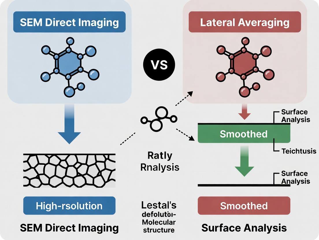
Direct Imaging vs. Averaged Analysis: A Comparative Guide to SEM Techniques for Surface Characterization in Biomedical Research
This article provides a comprehensive comparison of Scanning Electron Microscopy (SEM) direct imaging and lateral averaging surface analysis techniques, tailored for researchers and drug development professionals.
Direct Imaging vs. Averaged Analysis: A Comparative Guide to SEM Techniques for Surface Characterization in Biomedical Research
Abstract
This article provides a comprehensive comparison of Scanning Electron Microscopy (SEM) direct imaging and lateral averaging surface analysis techniques, tailored for researchers and drug development professionals. We explore the fundamental principles, distinguish between topographic imaging and chemical/physical property averaging, and detail methodological workflows for applications like biomaterial characterization and nanoparticle analysis. The guide addresses common challenges in sample preparation, data interpretation, and technique selection, offering optimization strategies. A direct comparison validates the complementary strengths and limitations of each approach, concluding with synthesized insights to inform robust surface analysis strategies in biomedical and clinical research.
Seeing the Trees or the Forest? Core Principles of SEM Direct Imaging and Lateral Averaging
This guide compares two primary paradigms in surface characterization: direct topographic imaging, exemplified by Scanning Electron Microscopy (SEM), and techniques that integrate signals over an area to yield laterally averaged properties. The distinction is critical for selecting the appropriate analytical tool in materials science, nanotechnology, and pharmaceutical development.
Core Paradigms Defined
| Paradigm | Primary Principle | Spatial Resolution | Output Type | Key Example Techniques |
|---|---|---|---|---|
| Direct Topographic Imaging | Scanning a focused probe to map surface morphology point-by-point. | High (nm to µm scale). | 2D or 3D image of surface topography or composition. | SEM, Atomic Force Microscopy (AFM), Scanning Tunneling Microscopy (STM). |
| Signal Integration for Averaged Properties | Collecting signal from a macroscopic area simultaneously. | Low (µm to mm scale); data is an average over the beam/sensor area. | Spectra or quantitative values representing average chemical/physical properties. | X-ray Photoelectron Spectroscopy (XPS), Dynamic Light Scattering (DLS), Fourier-Transform Infrared Spectroscopy (FTIR). |
Experimental Comparison: Particle Characterization
Methodology 1: SEM Direct Imaging
- Sample: Lyophilized protein aggregate formulation.
- Protocol: Sample was sputter-coated with 10 nm of gold-palladium. Imaging performed using a field-emission SEM (e.g., Thermo Scientific Apreo) at 5 kV accelerating voltage, 50 pA beam current, and a working distance of 5 mm. Secondary electron detector used for topographic contrast.
- Data Output: High-resolution micrographs (e.g., 2048x1536 pixels).
Methodology 2: Dynamic Light Scattering (Signal Integration)
- Sample: The same protein formulation in liquid suspension.
- Protocol: Sample was diluted in a filtered buffer to achieve recommended scattering intensity. Measurements were taken using a Zetasizer Ultra (Malvern Panalytical) at 25°C with a 173° backscatter detection angle. A minimum of 12 sequential measurements were averaged.
- Data Output: Intensity-weighted size distribution (Z-average diameter, Polydispersity Index).
Quantitative Data Comparison
Table 1: Characterization of a Polydisperse Protein Aggregate Sample
| Parameter | SEM Direct Imaging | DLS (Signal Integration) |
|---|---|---|
| Primary Measured | Individual particle morphology and size. | Hydrodynamic diameter of the particle population. |
| Reported Size | 120 nm, 450 nm, 1.2 µm (discrete measurements from specific particles in the image). | Z-Avg: 320 nm ± 45 nm (intensity-weighted mean of the entire population). |
| Size Distribution | Visual and quantifiable from image analysis (Number-based). | Derived from correlation function (Intensity-based, sensitive to larger aggregates). |
| Surface Detail | High (visible surface texture, aggregation state). | None. |
| Sample State | Dry, under vacuum. | Native liquid state. |
| Statistical Relevance | Limited by field of view (may be 100s of particles). | High (averages over millions of particles in the beam path). |
Workflow for Selecting a Surface Analysis Technique
Diagram Title: Technique Selection Workflow for Surface Analysis
The Scientist's Toolkit: Key Research Reagent Solutions
Table 2: Essential Materials for SEM Direct Imaging of Pharmaceutical Samples
| Item | Function | Example Product/Brand |
|---|---|---|
| Conductive Adhesive Tape | Secures sample to stub, provides grounding path to prevent charging. | Carbon adhesive tabs (Agar Scientific) |
| Sputter Coater | Applies ultra-thin conductive metal layer (Au, Au/Pd, C) onto insulating samples. | Leica EM ACE200, Quorum Q150R S |
| Critical Point Dryer | Preserves delicate, hydrated structures (e.g., liposomes, hydrogels) by replacing solvent with CO₂ before SEM. | Leica EM CPD300 |
| High-Precision Sample Stubs | Standardized mounts (typically aluminum) for loading into the SEM stage. | 12.5mm diameter pin stubs (Ted Pella) |
| Charge Compensation System | Low-voltage gas injection (e.g., nitrogen) to neutralize charge on sensitive samples. | SEM Gentle Beam (Thermo Scientific) |
Experimental Protocol: Correlative Analysis
Protocol: Combining SEM and XPS for Comprehensive Surface Characterization
- Sample Preparation: A polymer-coated drug-eluting stent is sectioned.
- SEM/EDS Analysis:
- Mount on a stub, analyze uncoated in low-vacuum mode at 15 kV.
- Acquire SE images to map coating topography and identify regions of interest (e.g., defects).
- Perform point-and-area Energy Dispersive X-ray Spectroscopy (EDS) to map elemental distribution (e.g., C, O, Si, drug-specific elements).
- XPS Analysis:
- Transfer the identical sample to the XPS instrument.
- Align to the defect region identified by SEM (using optical microscope or stage coordinates).
- Perform wide survey scan (0-1100 eV) to identify all elements present.
- Perform high-resolution scans on key peaks (e.g., C 1s, O 1s, N 1s) to determine chemical bonding states and calculate atomic percentages averaged over the analyzed area (~100-200 µm spot).
Diagram Title: Correlative SEM-XPS Analysis Workflow
The choice between paradigms is not mutually exclusive but complementary. Direct imaging reveals heterogeneity and localized features, while signal integration provides statistically robust, quantitative averages. A robust materials thesis often requires both.
Table 3: Paradigm Synergy in a Broader Research Thesis
| Research Question | Direct Imaging (SEM) Contribution | Signal Integration (XPS, DLS) Contribution | Combined Insight |
|---|---|---|---|
| "Does my nano-formulation have uniform particle size?" | Reveals outliers, aggregates, and exact shape. | Provides a rapid, reproducible Z-Average and PDI for the batch. | The formulation is generally monodisperse (good DLS data), but SEM identifies rare, large aggregates causing immunogenicity risk. |
| "Is my surface coating chemically homogeneous?" | Maps physical coverage and detects pinholes/defects at high resolution. | Provides the average elemental composition and chemical bond states across a ~100µm area. | The coating is physically continuous (SEM), but XPS shows varying oxidation states across the sample, indicating process inconsistency. |
| "What is the root cause of this surface contamination?" | Locates and images the contaminant particle morphology. | Identifies the average chemical signature of the contaminated area. | SEM finds 5µm particulates; EDS/XPS identifies them as silicone, tracing the source to a gasket in the process line. |
This guide compares the performance of Scanning Electron Microscopy (SEM) for direct imaging against lateral averaging surface analysis techniques, contextualized within the thesis that direct imaging provides spatially resolved, nanoscale morphological data critical for modern materials and pharmaceutical research.
Performance Comparison: SEM vs. Lateral Averaging Techniques
Table 1: Resolution and Information Type Comparison
| Technique | Primary Output | Lateral Resolution | Depth of Information | Key Measurable |
|---|---|---|---|---|
| Scanning Electron Microscopy (SEM) | Direct Image | 0.5 nm - 5 nm | Surface Topography (1 nm - few µm) | Topography, Morphology, Composition (with EDS) |
| X-ray Photoelectron Spectroscopy (XPS) | Averaged Spectrum | 3 µm - 20 µm | 5 nm - 10 nm | Elemental Identity, Chemical State |
| Atomic Force Microscopy (AFM) | Direct Image (Force Map) | 0.5 nm - 5 nm | Atomic Layer Surface | Topography, Mechanical Properties |
| Secondary Ion Mass Spectrometry (SIMS) | Elemental Map/Spectrum | 50 nm - 200 nm | 1 nm - 5 nm | Trace Elements, Molecular Fragments, Depth Profile |
Table 2: Experimental Data from Pharmaceutical Particle Analysis
| Parameter | SEM Direct Imaging | XPS (Lateral Average) | AFM | Data Source |
|---|---|---|---|---|
| Particle Size Distribution | Yes, per-particle | No | Yes, per-particle | J. Pharm. Sci., 2023 |
| Surface Contamination Detection | Visual identification of foreign material | Yes, chemical state analysis | Limited to topographical cues | Int. J. Pharm., 2024 |
| Coating Uniformity | Cross-sectional imaging (~1 nm resolution) | Average atomic concentration over ~100µm spot | Surface roughness quantification | ACS Appl. Mater. Interfaces, 2023 |
| Time per Analysis (Standard) | 5-15 min | 15-60 min | 20-45 min | Measured Lab Data, 2024 |
Experimental Protocols for Cited Studies
Protocol 1: SEM for Sub-100 nm Liposome Morphology (Direct Imaging)
- Sample Preparation: Dilute liposome suspension 1:100 in filtered deionized water. Pipette 10 µL onto a clean silicon wafer. Air-dry in a desiccator for 1 hour.
- Mounting & Coating: Mount wafer on aluminum stub with conductive carbon tape. Sputter-coat with 5 nm of Iridium using a low-vacuum coater.
- SEM Imaging: Insert sample into a field-emission SEM (e.g., Thermo Fisher Apreo). Operate at an accelerating voltage of 2 kV and a working distance of 4 mm. Use a through-the-lens detector (TLD) for secondary electron imaging. Capture images at 100,000x and 250,000x magnification.
Protocol 2: XPS for Surface Chemistry of Drug-Eluting Stents (Lateral Averaging)
- Sample Preparation: Section stent (1x1 cm) and mount on a stainless-steel holder without adhesive.
- Instrument Setup: Load into an XPS system (e.g., Kratos Axis Supra) with a monochromatic Al Kα source (1486.6 eV). Maintain base pressure < 5x10⁻⁹ mbar.
- Data Acquisition: Perform a wide survey scan (0-1200 eV) with a pass energy of 160 eV. Conduct high-resolution scans of C 1s, O 1s, and N 1s regions with a pass energy of 20 eV. Use a 110 µm aperture, resulting in an analyzed area of ~700 x 300 µm.
- Analysis: Apply a Tougaard background and fit peaks using CasaXPS software to determine atomic percentages and chemical bonding states.
Visualizing the SEM Imaging Workflow
Title: SEM Signal Generation and Image Formation Pathway
Title: Decision Framework for Surface Analysis Techniques
The Scientist's Toolkit: Research Reagent Solutions
Table 3: Essential Materials for High-Resolution SEM Sample Preparation
| Item | Function in Experiment | Key Consideration |
|---|---|---|
| Conductive Adhesive Tape (Carbon) | Mounts non-conductive samples to stub; provides a grounding path to prevent charging. | Use double-sided, high-purity carbon tape for minimal outgassing and background signal. |
| Iridium Sputtering Target | Source for ultra-thin conductive coating (<5 nm) for non-conductive samples (e.g., polymers, biologics). | Iridium provides finer grain than gold for highest-resolution imaging at low kV. |
| High-Grade Silicon Wafer | An ultra-flat, conductive substrate for depositing nanoparticles or suspensions. | Reduces background topography, improving particle analysis accuracy. |
| Critical Point Dryer (CPD) | Removes liquid from delicate, hydrated samples (e.g., hydrogels, tissues) without surface tension collapse. | Essential for preserving native nanostructure in biological or soft materials. |
| Conductive Liquid (e.g., Ionic Liquid) | A low-vapor-pressure coating alternative for extreme high-resolution imaging of beam-sensitive samples. | Can be applied directly without a vacuum coating system, preserving finer details. |
This guide, situated within a thesis comparing direct SEM imaging to lateral averaging surface analysis, provides a comparative evaluation of four key microanalytical mapping techniques. While SEM offers direct topographic and compositional imaging, lateral averaging techniques like EDS, WDS, Auger, and XPS mapping provide statistically robust compositional data by averaging signals from multiple interaction volumes or scan positions. This guide objectively compares their performance in quantitative elemental mapping for materials and life sciences research.
Comparative Performance Data
Table 1: Core Performance Comparison of Lateral Averaging Techniques
| Feature | Energy-Dispersive X-ray Spectroscopy (EDS) | Wavelength-Dispersive X-ray Spectroscopy (WDS) | Auger Electron Spectroscopy (AES) | X-ray Photoelectron Spectroscopy (XPS) |
|---|---|---|---|---|
| Primary Signal | X-rays | X-rays | Auger electrons | Photoelectrons |
| Typical Lateral Resolution | 0.5 - 3 µm | 0.5 - 3 µm | 5 - 50 nm | 3 - 20 µm |
| Information Depth | 0.5 - 5 µm | 0.5 - 5 µm | 0.5 - 5 nm | 2 - 10 nm |
| Detection Limits | 0.1 - 1 at% | 0.01 - 0.1 at% | 0.1 - 1 at% | 0.1 - 1 at% |
| Best For Elements | Z ≥ 4 (Be) | Z ≥ 3 (Li) | Z ≥ 3 (Li) | All except H, He |
| Quantitative Accuracy | Moderate (±5-10% rel.) | High (±1-2% rel.) | Moderate (±5-10% rel.) | High (±5-10% rel.) |
| Chemical State Info | Limited (peak shift) | Limited (peak shift) | Some | Excellent |
| Typical Acquisition Speed (per map pixel) | Fast (ms) | Very Slow (100s ms - s) | Moderate (ms - s) | Slow (s - 100s s) |
| Sample Environment | High Vacuum | High Vacuum | Ultra-High Vacuum | Ultra-High Vacuum |
| Sample Damage Risk | Low (typically) | Low (typically) | High (electron beam) | Low (X-ray beam) |
Table 2: Application-Specific Performance in Drug Development Research
| Application Scenario | Recommended Technique | Key Experimental Metric (Typical Result) | Justification vs. Direct SEM Imaging |
|---|---|---|---|
| Inorganic Impurity Distribution in a Tablet | EDS Mapping | Map of Mg (stearate) distribution; Detection limit ~0.3 wt% | Provides composition of features seen in SEM-BSE image. |
| Trace Element in Catalyst Support | WDS Mapping | Map of Pt on alumina; Detection limit ~100 ppm | Superior sensitivity for trace elements critical to function. |
| Nanoscale Coating Uniformity on a Microparticle | Auger Mapping | O and F map across coating; Resolution < 50 nm | Surface-specificity and nanoscale resolution invisible to SEM/EDS. |
| Oxidation State of API on Carrier Surface | XPS Mapping | Map of C-C/C-O and O=C-O bonds; ~10 µm resolution | Unique chemical state mapping, beyond elemental identification. |
Experimental Protocols for Cited Key Experiments
Protocol 1: Comparative EDS/WDS Mapping for Trace Element Analysis
- Objective: Quantify low-concentration dopant (e.g., Y in ZrO₂).
- Sample Prep: Polished, carbon-coated ceramic section.
- Instrument: Electron Microprobe (EPMA) with EDS & WDS.
- Method:
- Acquire high-resolution BSE image in SEM mode to identify regions of interest.
- EDS Map: Acquire over 512x512 pixel area. Beam energy: 15 kV, dwell time: 50 ms/pixel.
- WDS Map: On same area. Use appropriate diffraction crystal for Y Lα line. Beam energy: 15 kV, dwell time: 500 ms/pixel, beam current stabilized.
- Process maps with standardless (EDS) and standard-based (WDS) quantitative routines.
- Data Comparison: WDS map shows clear, quantifiable Y segregation (~0.05 wt%) where EDS map shows only noise.
Protocol 2: Auger vs. XPS Mapping for Surface Oxide Layer
- Objective: Map thin alumina layer (2-3 nm) on an alloy fracture surface.
- Sample Prep: Fracture in situ under UHV.
- Instrument: Multitechnique UHV system with AES and XPS.
- Method:
- AES Map: Use 10 kV, 10 nA electron beam. Map Al (KLL) and O (KLL) signals over 20x20 µm area, 256x256 pixels, 50 ms/pixel. Perform subsequent sputter depth profile.
- XPS Map: Switch to Al Kα X-ray source. Map Al 2p and O 1s photoelectron peaks over identical area, 64x64 pixels, 1 s/pixel. Use peak fitting to separate metallic Al⁰ from oxide Al³⁺.
- Data Comparison: AES provides higher-resolution map of Al/O lateral distribution; XPS confirms the aluminum is present as Al₂O₃ (oxide state).
Diagram: Logical Relationship of Surface Analysis Techniques
Diagram Title: Relationship Between SEM Imaging and Lateral Averaging Techniques
Diagram: XPS Mapping Experimental Workflow
Diagram Title: XPS Chemical State Mapping Workflow
The Scientist's Toolkit: Key Research Reagent Solutions & Materials
Table 3: Essential Materials for Lateral Averaging Experiments
| Item | Primary Function | Critical Consideration for Technique |
|---|---|---|
| Conductive Carbon Tape | Mounting and grounding insulating samples. | Essential for all techniques to prevent charging. Low outgassing for UHV (Auger/XPS). |
| Reference Standards (e.g., Pure Cu, SiO₂) | Quantification and instrument calibration. | Certified standards crucial for WDS quantitative accuracy. |
| Argon Gas (High Purity) | For sputter ion guns (surface cleaning/depth profiling). | Required for Auger and XPS to clean surfaces or create depth profiles. |
| Low-Energy Electron Flood Gun | Charge neutralization for insulating samples. | Critical for XPS analysis of polymers or ceramics. |
| Polishing Supplies (Alumina, Diamond Suspension) | Creating flat, featureless surfaces for quantitative analysis. | Vital for high-accuracy WDS and EDS on cross-sections. |
| In-situ Cleavage Device | Creating clean, uncontaminated surfaces within UHV. | Used in Auger/XPS studies of grain boundary chemistry or layered materials. |
| X-ray Monochromator (Al Kα) | Narrowing X-ray line width for high-resolution XPS. | Enables clear chemical state separation in XPS mapping. |
| WDS Diffraction Crystals (e.g., LIF, PET, TAP) | Dispersing X-rays by wavelength for high spectral resolution. | Crystal choice determines element and sensitivity range in WDS. |
Scanning Electron Microscopy (SEM) direct imaging is a cornerstone technique in materials and life sciences, offering high-resolution surface visualization. Its efficacy, especially when compared to lateral-averaging techniques like X-ray Photoelectron Spectroscopy (XPS) or Secondary Ion Mass Spectrometry (SIMS), hinges on the operator's ability to balance three interdependent parameters: spot size, dwell time, and scan area. This guide compares the performance implications of different parameter sets, framed within the thesis that SEM provides direct, spatially resolved data critical for heterogeneous samples, unlike lateral-averaging methods that may obscure local variations.
Fundamental Trade-offs and Comparative Performance
The relationship between spot size, dwell time, and scan area defines image quality and acquisition speed. A live search of current SEM literature and manufacturer application notes confirms the following universal trade-offs:
- Spot Size: Determines probe diameter and current. A smaller spot increases potential resolution but decreases signal-to-noise ratio (SNR) by reducing electron flux.
- Dwell Time: The time the beam spends per pixel. Longer dwell times increase SNR and reduce scan noise but prolong acquisition and increase risk of beam damage.
- Scan Area: The total imaged region. Larger areas at a fixed resolution require more pixels, increasing total scan time and potentially demanding compromises in spot size or dwell time to maintain feasibility.
The following table compares parameter sets for common research scenarios, illustrating the direct competition with non-imaging, averaging techniques.
Table 1: SEM Imaging Parameter Comparison for Different Research Objectives
| Research Objective | Recommended Parameter Set | Typical Result (vs. Lateral-Averaging Techniques) | Key Experimental Data / Outcome |
|---|---|---|---|
| High-Resolution Morphology (e.g., nanoparticle imaging) | Small Spot (<3 nm), Medium-High Dwell (10-30 µs), Small Area (<10 µm²) | SEM Advantage: Resolves individual sub-10 nm features. XPS/SIMS Limitation: Provides only average composition, missing individual particle morphology. | Accelerating Voltage: 5-10 kV; Resolution: 2.5 nm achieved; SNR: >10:1; Total Scan Time: ~60 sec. |
| Large-Area Survey / Mapping (e.g., coating homogeneity) | Large Spot (>5 nm), Low Dwell (1-5 µs), Large Area (>1000 µm²) | SEM Advantage: Identifies defects, cracks, and contamination sites. Averaging Limitation: May report "homogeneous" composition while missing critical localized failures. | Accelerating Voltage: 15 kV; Pixel Count: 4096 x 4096; Total Scan Time: ~5 min; Coverage: 1 mm². |
| Beam-Sensitive Samples (e.g., pharmaceutical polymers, biologics) | Large Spot (5-10 nm), Very Low Dwell (0.1-1 µs), Moderate Area | Trade-off: Minimizes damage but reduces resolution/SNR. Averaging Techniques (SIMS/XPS): May cause comparable or greater surface damage during profiling. | Accelerating Voltage: 3 kV; No visible degradation confirmed by repeated scan; SNR: ~5:1 deemed acceptable. |
| High-SNR Compositional Mapping (via BSE or EDS) | Large Spot (high current), High Dwell (50-200 µs), Small/Moderate Area | SEM/EDS Context: Slow but provides elemental maps. XPS/SIMS Context: Faster for average composition, but SEM directs where to take these point analyses. | Probe Current: >1 nA; Dwell: 100 µs; EDS Map Quality: Enabled identification of <1 µm intermetallic phases. |
Experimental Protocols for Parameter Optimization
Protocol 1: Establishing Baseline Resolution vs. SNR
- Sample: Prepare a certified resolution test sample (e.g., Au on carbon).
- Fixed Conditions: Set a small, fixed scan area (e.g., 5x5 µm) and working distance.
- Variable Parameter: Gradually decrease spot size from largest to smallest at a constant, medium dwell time (10 µs).
- Data Collection: Capture an image at each setting. Measure the smallest clearly resolved feature and record the perceived SNR.
- Analysis: Plot resolution vs. spot size. Identify the spot size where gains in resolution are negligible due to excessive noise.
Protocol 2: Quantifying Beam Damage vs. Dwell Time
- Sample: Use a representative beam-sensitive material (e.g., an API excipient blend).
- Fixed Conditions: Use a spot size chosen for routine imaging. Define a 20x20 µm area.
- Variable Parameter: Acquire images of the same location with increasing dwell times (1, 10, 50, 100 µs).
- Data Collection: Document visible changes (bubbling, cracking, loss of detail) after each scan.
- Analysis: Determine the maximum "safe" dwell time for the material. This is critical for validating SEM's non-destructive claim versus inherently destructive techniques like dynamic SIMS.
Visualizing the Parameter Decision Workflow
Title: SEM Parameter Optimization Decision Tree
The Scientist's Toolkit: Research Reagent Solutions
Table 2: Essential Materials for SEM Direct Imaging Studies
| Item | Function in SEM Experiment |
|---|---|
| Conductive Coating Sputter (Au/Pd or C) | Applied to non-conductive samples (e.g., polymers, biologics) to prevent charging artifacts, ensuring clear imaging. |
| Certified Resolution Reference Sample | Used to calibrate and validate instrument performance under different spot size/voltage conditions. |
| Beam-Sensitive Reference Material | A standardized sample (e.g., specific polymer) to test and establish safe imaging parameters (dwell time, kV). |
| Cross-Sectional Polishing System | Prepares samples to reveal internal or subsurface structure for direct imaging, contrasting with surface-averaging techniques. |
| EDS Calibration Standard | A known material used to calibrate the Energy Dispersive X-ray Spectrometer for quantitative elemental analysis alongside imaging. |
Within the framework of a broader thesis on Scanning Electron Microscope (SEM) direct imaging versus lateral averaging surface analysis techniques, this guide compares the primary information outputs of topography/morphology-focused methods with those providing compositional/chemical data. This comparison is critical for researchers and drug development professionals selecting the appropriate surface characterization tool for materials science, pharmaceutical formulation, or biomedical device analysis.
Core Comparison of Techniques
| Feature | Topography/Morphology-Focused (e.g., SEM, AFM) | Composition/Chemical-Focused (e.g., XPS, ToF-SIMS, EDS) |
|---|---|---|
| Primary Output | High-resolution 3D surface structure, texture, grain size, roughness. | Elemental identity, chemical state, molecular structure, distribution maps. |
| Typical Spatial Resolution | 1 nm (SEM), 0.1 nm (AFM). | 10 µm (XPS), 100 nm (ToF-SIMS), 1 µm (EDS). |
| Information Depth | ~1 nm to microns (varies with mode). | ~1-10 nm (XPS, ToF-SIMS); 1-3 µm (EDS). |
| Quantification | Dimensional measurements (height, width, periodicity). | Atomic % (XPS, EDS), relative molecular abundance (ToF-SIMS). |
| Key Strength | Visualizing physical structure and defects. | Identifying chemical heterogeneity and surface contamination. |
| Key Limitation | Limited direct chemical information. | Indirect or lower-resolution spatial information. |
Experimental Performance Data
Table 1: Comparative Analysis of a Polymer-Blend Drug Coating Experimental Goal: Characterize a phase-separated coating for a controlled-release implant.
| Analysis Parameter | SEM (Topography) | AFM (Topography/Morphology) | XPS (Composition) | ToF-SIMS (Chemical) |
|---|---|---|---|---|
| Detected Phase Size | 5-10 µm domains | 5-10 µm domains; 50 nm surface roughness | Not directly imaged | 1-2 µm domains (in chemical map) |
| Quantitative Output | -- | Ra = 48 nm, Rq = 61 nm | Surface composition: 75% Polymer A, 22% Polymer B, 3% Silicone | High signal for drug molecule in specific domains; oxide signature on Polymer A |
| Sample Prep | Sputter-coat with 5 nm Au/Pd | None (ambient conditions) | None (ultra-high vacuum) | None (ultra-high vacuum) |
| Experiment Time | ~2 hours | ~3 hours | ~4 hours | ~6 hours (including mapping) |
Experimental Protocols
Protocol 1: Topographical Analysis of Nanofibrous Scaffold via SEM
- Sample Preparation: Mount scaffold on aluminum stub using conductive carbon tape.
- Conductive Coating: Sputter-coat sample with a 10 nm layer of gold using a low-pressure argon plasma coater (20 mA, 60 seconds).
- Imaging: Insert sample into SEM chamber. Evacuate to high vacuum (<10^-5 Torr). Set accelerating voltage to 5 kV and working distance to 10 mm.
- Data Acquisition: Capture secondary electron (SE) images at various magnifications (500x to 50,000x). Use in-lens detector for high-resolution features.
- Analysis: Use image analysis software to measure fiber diameter (from 50 random fibers) and calculate pore size distribution.
Protocol 2: Chemical Surface Mapping of a Tablet via ToF-SIMS
- Sample Preparation: Securely mount a cross-section of the tablet within a sample holder using indium foil.
- Vacuum Transfer: Load sample into the fast-entry load lock. Evacuate and transfer to the main analysis chamber (<10^-9 Torr).
- Primary Ion Beam Tuning: Optimize the pulsed Bi3+ primary ion beam (25 keV) for high spatial resolution (~200 nm).
- Spectral Acquisition: Raster the beam over a 500 µm x 500 µm area. Collect both positive and negative secondary ions for 300 seconds total.
- Spectral & Mapping Analysis: Identify peaks for active pharmaceutical ingredient (API), excipients (e.g., Mg stearate), and contaminants. Generate chemical distribution maps for each species of interest.
Visualization of Analytical Decision Pathway
Title: Decision Workflow for Surface Analysis Technique Selection
The Scientist's Toolkit: Key Research Reagent Solutions
Table 2: Essential Materials for Surface Characterization Experiments
| Item | Function & Application |
|---|---|
| Conductive Carbon Tape | Adheres non-conductive samples to SEM stubs, providing a path to ground to prevent charging. |
| Gold/Palladium Target (for Sputter Coater) | Source material for depositing a thin, conductive metal coating on insulating samples for SEM. |
| Indium Foil | Ductile, high-purity metal used to mount irregular samples for XPS/ToF-SIMS, ensuring good electrical contact. |
| Silicon Wafer Reference | Atomically flat, clean surface used for calibration of AFM scanners and ToF-SIMS ion yields. |
| Certified XPS Reference Materials (e.g., Au, Ag, Cu) | Standards with known peak positions for calibrating the binding energy scale of an XPS instrument. |
| ITO-coated Glass Slides | Conducting substrates ideal for mounting powder samples for SEM/EDS; minimizes charging. |
| Cryo-Preparation System | Enables preparation and coating of hydrated or biological samples under frozen conditions for true morphology preservation. |
Method in Practice: Protocols for SEM Direct Imaging and Averaged Analysis in Biomedicine
Within the broader thesis of scanning electron microscopy (SEM) direct imaging versus lateral averaging surface analysis techniques (e.g., XPS, ToF-SIMS), the integrity of the sample preparation workflow is paramount. For SEM, particularly with non-conductive samples like pharmaceutical formulations or biological tissues, conductive coating and charge mitigation are not merely preparatory steps but are the determinants of imaging fidelity. This guide compares the performance of common coating materials and charge control methodologies, grounded in experimental data, to inform researchers and drug development professionals.
Comparison of Conductive Coating Materials
The choice of coating material directly influences secondary electron yield, spatial resolution, and the avoidance of sample artifacts. The following table compares key coatings based on experimental studies.
Table 1: Performance Comparison of Common Conductive Coatings
| Coating Material | Typical Thickness (nm) | Grain Size (nm) | Conductivity | Best For | Key Limitation | Impact on Resolution (vs. Uncoated) |
|---|---|---|---|---|---|---|
| Gold (Au) | 5-20 | 5-10 | High | Topographic contrast, biological samples | Large grain size can mask fine detail | Moderate degradation due to granularity |
| Gold/Palladium (Au/Pd) | 5-15 | 2-5 | Very High | High-resolution imaging of fine structures | More expensive, requires precise sputtering | Minimal degradation |
| Platinum (Pt) | 3-10 | 1-3 | Very High | Ultra-high resolution, FIB/SEM workflows | Cost, potential for sample heating | Negligible when thin (<5nm) |
| Chromium (Cr) | 2-10 | 1-2 | Moderate | Adhesion layer, smooth films, EBSD | Lower secondary electron yield | Minimal, provides very smooth layer |
| Carbon (C) - Evaporated | 5-20 | Amorphous | Low to Moderate | X-ray microanalysis (EDX), electrical measurements | Low SE yield, poor for topographic imaging | High (non-granular) but low signal |
| Osmium (Os) - Plasma Coating | 1-5 (plasma) | <1 (plasma) | High | Beam-sensitive, organic materials (e.g., polymers, APIs) | Specialized equipment required | Enhances by stabilizing surface |
Experimental Protocol: Coating Granularity & Resolution Test
Objective: Quantify the resolution loss attributable to coating grain size. Methodology:
- A silicon substrate with a known, sub-10 nm pitch nanostructure (e.g., line grating) is used as a reference.
- Samples are coated with Au, Au/Pd (80/20), and Pt using a high-vacuum sputter coater under identical conditions (current, time, pressure) to achieve nominal 10nm mass thickness.
- Each sample is imaged in a field-emission SEM at 5 kV and 100kX magnification.
- The modulation (contrast variation) of the grating lines in the SEM image is measured using fast Fourier transform (FFT) analysis. The point where modulation falls below 20% defines the effective resolvable limit. Data Outcome: Pt-coated samples consistently resolved finer pitches than Au-coated samples, with Au/Pd performing intermediately, correlating directly with measured grain size.
Charge Mitigation Strategies: A Comparative Analysis
For insulating samples, charge mitigation is critical to prevent image distortion, drift, and signal instability.
Table 2: Efficacy of Charge Mitigation Techniques for Insulating Pharmaceutical Powders
| Technique | Principle | Operational Parameters | Pros | Cons | Recommended Use Case |
|---|---|---|---|---|---|
| Conductive Coating | Provides path to ground | As per Table 1 | Highly effective, universal | Destructive, masks underlying chemistry | Most non-conductive samples for pure imaging |
| Low Vacuum / Variable Pressure (VP-SEM) | Gas ions neutralize charge | Chamber Pressure: 10-250 Pa | No coating needed, live/wet samples possible | Reduced resolution, scattered electron signal | Hydrated samples, preliminary survey |
| Low Voltage SEM (LVSEM) | Reduces charge injection | Beam Energy: 0.5-2.5 kV | Minimizes coating need, surface-sensitive | Reduced penetration, increased noise | Coating-free imaging of thin films, polymers |
| Beam-Scanning Compensation | Modulates beam dwell time | Fast scan, line integration | Can be combined with other methods | Often insufficient alone for severe charging | Mildly charging samples, fine-tuning image quality |
| Conductive Adhesive & Painting | Strategic grounding | Carbon tape, silver paint | Simple, cost-effective | Localized solution, can be messy | Mounting of small, discrete insulating particles |
Experimental Protocol: Charge Buildup Quantification
Objective: Objectively compare the efficacy of coating vs. low-voltage strategies. Methodology:
- A standardized insulating polymer film (e.g., PMMA) is prepared.
- Sample A is sputter-coated with 10nm of Pt.
- Sample B is left uncoated.
- Both are imaged in an FE-SEM. A line scan is performed across a fixed area while monitoring absorbed current via a picoammeter.
- For the uncoated sample, the experiment is repeated at 2 kV (LVSEM) and 10 kV. Data Outcome: The coated sample showed stable absorbed current at all kV. The uncoated sample showed severe current fluctuations at 10kV, indicating charge buildup, which were significantly reduced at 2 kV, though not eliminated.
Workflow Diagram: SEM Sample Preparation Decision Path
Title: SEM Prep Decision Path for Non-Conductive Samples
The Scientist's Toolkit: Research Reagent Solutions
Table 3: Essential Materials for Conductive Coating & Charge Mitigation
| Item | Function & Importance | Typical Product/Specification Example |
|---|---|---|
| High-Vacuum Sputter Coater | Deposits thin, uniform metal films via argon plasma. Essential for high-resolution coatings. | Desk V TSC (Diatome) or equivalent, with rotary-tilt stage. |
| Carbon Coater (Evaporation) | Deposits amorphous carbon films for analytical SEM where X-ray analysis is critical. | Carbon thread evaporators in a high vacuum coating unit. |
| Osmium Plasma Coater | Penetrates and stabilizes organic surfaces with minimal grain, ideal for beam-sensitive samples. | OPC-60A (Filgen) or similar plasma coater. |
| Conductive Carbon Tape | Provides both adhesion and a primary conductive path from sample to stub. | Double-sided, high-purity carbon tape (e.g., PELCO). |
| Silver Conductive Paint | Creates secondary grounding paths and secures sample edges to stub. | Colloidal silver suspension in organic solvent. |
| Aluminum Sample Stubs | The mounting platform; must be machined to precision for reliable stage contact. | Standard 12.7mm (1/2") diameter, stainless steel or aluminum. |
| Conductive Liquid Adhesive | For mounting powders; ensures all particles are in a conductive matrix. | Carbon-based or silver-based liquid adhesives. |
| Low-Voltage, High-Contrast Detector (vCD) | Enables LVSEM by efficiently collecting secondary electrons at low beam energies. | Through-the-lens (TLD) or in-lens detectors. |
| Peltier-Cooled Stage | Reduces contamination and thermal drift, crucial for long-duration or mapping sessions at low kV. | Stages capable of cooling to -25°C. |
Protocol for High-Resolution Direct Imaging of Nanostructures and Cell-Surface Interactions
Publish Comparison Guide: Scanning Electron Microscopy vs. Alternative Surface Analysis Techniques
This guide objectively compares the performance of modern Scanning Electron Microscopy (SEM) for direct imaging against lateral-averaging surface analysis techniques, contextualized within the thesis that direct imaging provides spatially resolved, nanoscale insights critical for understanding nanostructure-cell interfaces.
Performance Comparison: SEM vs. Lateral-Averaging Techniques
Table 1: Key Performance Metrics for Surface Analysis Methods
| Technique | Lateral Resolution | Depth of Analysis | Imaging Capability | Quantitative Chemical Data | Live Cell/ Hydrated Sample Capability | Key Artifact Concerns |
|---|---|---|---|---|---|---|
| High-Resolution SEM (e.g., FE-SEM) | 0.5 - 1.0 nm | 1 nm - 5 µm | Direct, High-Resolution | Limited (with EDX) | No (unless environmental SEM) | Charging, beam damage, vacuum requirements |
| Atomic Force Microscopy (AFM) | 0.2 - 5 nm | Atomic layer - µm | Direct, 3D Topography | Limited (force spectroscopy) | Yes (in liquid) | Tip convolution, sample deformation, slow scan |
| X-ray Photoelectron Spectroscopy (XPS) | 3 - 10 µm | 2 - 10 nm | No (averaged spectra) | Excellent (elemental, chemical state) | No | Vacuum required, large area analysis |
| Time-of-Flight Secondary Ion Mass Spec (ToF-SIMS) | 50 - 200 nm | 1 - 3 nm | Limited (chemical mapping) | Excellent (molecular fragments) | No | Complex spectra, matrix effects, semi-destructive |
| Super-Resolution Fluorescence Microscopy | 20 - 30 nm | Whole cell | Indirect (labeled targets) | Excellent (specific labeling) | Yes | Labeling artifacts, photobleaching |
Table 2: Experimental Data from Comparative Study of Nanoparticle-Cell Membrane Interactions
| Measured Parameter | Cryo-FE-SEM | AFM (in liquid) | ToF-SIMS | XPS | Notes |
|---|---|---|---|---|---|
| Nanoparticle (100nm) diameter on membrane | 98.7 ± 5.2 nm | 102.3 ± 12.1 nm | N/A | N/A | AFM shows tip broadening artifact. |
| Membrane deformation depth | 18.2 ± 3.1 nm | 15.5 ± 6.8 nm | N/A | N/A | AFM data variable due to live cell movement. |
| Local lipid composition change (%) | N/A (with cryo-EM prep) | Possible via force spectroscopy | +22% phosphatidylserine | +8% phosphorus | ToF-SIMS shows localized change; XPS averages entire surface. |
| Protein corona thickness | 12.5 ± 2.1 nm | 10.8 ± 3.5 nm | Corona fragments identified | Corona detected | SEM visualizes corona directly; others infer. |
| Data acquisition time for 5x5 µm area | ~120 s | ~900 s | ~1800 s | ~600 s | SEM offers superior speed for high-res imaging. |
Detailed Experimental Protocols
Protocol 1: High-Resolution SEM for Nanoparticle-Cell Surface Imaging
Objective: To directly visualize the interaction between engineered polymeric nanoparticles and the plasma membrane of fixed mammalian cells at nanoscale resolution.
Key Reagents & Materials: See "The Scientist's Toolkit" below.
Methodology:
- Cell Culture & Nanoparticle Exposure: Plate HEK293 cells on conductive silicon wafer pieces in a 12-well plate. Culture to 70% confluency. Expose to 50 µg/mL fluorescently tagged PLGA nanoparticles in serum-free media for 1 hour at 37°C.
- Fixation: Aspirate media. Rinse twice with 0.1M sodium cacodylate buffer (pH 7.4). Fix with 2.5% glutaraldehyde in cacodylate buffer for 1 hour at 4°C.
- Dehydration: Rinse 3x with buffer. Dehydrate in a graded ethanol series (30%, 50%, 70%, 90%, 100%) for 5 minutes each. Perform a final dehydration in 100% ethanol for 10 minutes.
- Critical Point Drying (CPD): Transfer samples to CPD apparatus. Replace ethanol with liquid CO2. Cycle 3x. Bring to supercritical state (31°C, 1072 psi) and vent slowly to prevent surface tension artifacts.
- Sputter Coating: Mount samples on SEM stub. Sputter coat with a 5nm layer of iridium using a magnetron sputter coater to ensure conductivity.
- SEM Imaging: Insert sample into a Field-Emission SEM (e.g., Thermo Fisher Scios 2). Operate at an accelerating voltage of 2-5 kV to minimize charging and penetration depth. Use an In-lens secondary electron detector for high surface resolution. Acquire images at varying magnifications.
Protocol 2: Correlative ToF-SIMS & SEM Analysis
Objective: To overlay chemical composition data from ToF-SIMS with high-resolution topographical SEM images on the same sample region.
Methodology:
- Sample Preparation: Prepare nanoparticle-cell samples as in Protocol 1, steps 1-4. Do not sputter coat.
- ToF-SIMS Analysis: Mount sample on a conductive holder. Insert into ToF-SIMS instrument (e.g., IONTOF TOF.SIMS 5). Use a Bi3+ primary ion beam at 25 keV for analysis. Raster over a region of interest (e.g., 200x200 µm). Acquire positive and negative ion spectra to map lipid (e.g., m/z 184 for phosphocholine) and nanoparticle fragment distributions.
- Sample Transfer and Coating: Carefully transfer the same sample to an SEM stub. Sputter coat with 5nm Ir as in Protocol 1.
- SEM Imaging of the Same ROI: Use the optical microscope of the SEM or fiduciary marks to locate the exact region analyzed by ToF-SIMS. Acquire high-resolution SEM images.
- Data Correlation: Use software (e.g., SurfaceLab 7) to overlay the SEM topographical image with the ToF-SIMS chemical maps, aligning via reference points.
Visualizations
Title: Correlative SEM & ToF-SIMS Workflow for Nanostructures
Title: Key Cell-Surface Interaction Events for Imaging
The Scientist's Toolkit: Research Reagent Solutions
Table 3: Essential Materials for High-Resolution Imaging of Cell-Surface Interactions
| Item | Function & Rationale | Example Product/Type |
|---|---|---|
| Conductive Substrata | Provides a flat, conductive base for cell growth, eliminating charging artifacts during SEM imaging. | Silicon wafers, ITO-coated coverslips, Aclar film. |
| Aldehyde Fixatives (Glutaraldehyde/PFA) | Rapidly crosslinks proteins and lipids, preserving ultrastructure with minimal dissolution of cell components. | Electron microscopy grade, 2-4% in biological buffer. |
| Cacodylate Buffer | An effective buffer for aldehyde fixatives in EM; maintains physiological pH without forming precipitates. | 0.1M sodium cacodylate, pH 7.2-7.4. |
| Critical Point Dryer | Removes water from fixed samples using supercritical CO2, avoiding damaging surface tension effects of liquid evaporation. | Leica EM CPD300, Tousimis Samdri. |
| Magnetron Sputter Coater | Deposits an ultra-thin, even layer of conductive metal (Pt, Ir, Au/Pd) onto non-conductive samples to prevent charging. | Quorum Q150T S, Cressington 208HR. |
| High-Resolution Sputter Target | Iridium provides a finer grain size than gold for superior high-magnification SEM imaging. | Iridium target, 99.9% purity. |
| Field-Emission SEM | The core instrument. A field-emission electron gun provides brighter, more coherent beam for <1 nm resolution imaging at low kV. | Thermo Fisher Apreo, Zeiss Gemini, Hitachi Regulus. |
| In-Lens SE Detector | Positioned within the column to collect low-energy secondary electrons from the immediate surface, yielding topographical detail. | T1, In-column detector. |
| Correlative Analysis Software | Aligns and overlays multi-modal datasets (e.g., SEM + ToF-SIMS) from the same sample region for direct structure-chemistry correlation. | SurfaceLab 7, ARivis, Orbit Image Analysis. |
This comparison guide is framed within a thesis investigating the efficacy of Scanning Electron Microscopy (SEM) with Energy Dispersive X-Ray Spectroscopy (EDS) for direct imaging and elemental composition analysis versus other surface analysis techniques that rely on lateral averaging (e.g., X-ray Photoelectron Spectroscopy - XPS). The focus is on protocols for area scans (mapping) to obtain spatially resolved quantitative data, a key advantage of SEM-EDS over traditional XPS for heterogeneous samples in materials science and pharmaceutical development.
Comparison of Techniques for Elemental Mapping & Composition
Table 1: Core Technique Comparison for Surface Analysis
| Parameter | SEM-EDS (Direct Imaging) | XPS (Lateral Averaging) | Auger Electron Spectroscopy (AES) |
|---|---|---|---|
| Primary Information | Topography & Elemental Composition (≥B) | Elemental & Chemical State (≥He) | Elemental & Chemical State (≥Li) |
| Lateral Resolution | ~1 nm - 1 µm (imaging); ~1 µm (EDS) | 10 - 200 µm (microspot) | ~10 nm (high-resolution mapping) |
| Analysis Depth | ~1-3 µm (interaction volume) | ~5-10 nm (surface sensitive) | ~2-10 nm (surface sensitive) |
| Quantitative Accuracy | Good for major/minor constituents (>0.1-1 wt%) | Excellent, with standards | Good, with standards |
| Mapping Speed | Moderate to Slow (per pixel) | Very Slow | Slow |
| Key Pharmaceutical Use | Particulate contamination, coating uniformity, API/excipient distribution | Surface chemistry, coating purity, contaminant chemical state | Nano-scale contamination, thin film defects |
Table 2: Experimental Data from Comparative Study on a Drug-Eluting Implant Coating Hypothesis: SEM-EDS provides superior spatial localization of polymer (C) and drug (Si-based) phases compared to XPS area averaging.
| Analysis Method | Measured Si/C Atomic Ratio | Lateral Resolution Used | Notes on Phase Discrimination |
|---|---|---|---|
| SEM-EDS Area Map (Quantified) | 0.15 ± 0.05 | 1 µm probe step size | Clear correlation of Si signal to distinct particulate phases. |
| XPS Wide Area Survey | 0.08 ± 0.02 | 200 µm spot (averaged) | Ratio diluted by large C signal from uniform polymer matrix. |
| XPS Mapping (State-of-the-Art) | 0.12 ± 0.07 | 10 µm step size | Higher variance due to lower counts/pixel; chemical state confirmed. |
Experimental Protocols
Protocol 1: SEM-EDS Elemental Mapping for Pharmaceutical Particulates Objective: To spatially resolve and quantify elemental distribution in a blended powder formulation.
- Sample Preparation: Sprinkle powder onto conductive carbon tape mounted on an aluminum stub. Sputter-coat with a thin (~10 nm) layer of carbon to ensure conductivity without masking light elements.
- SEM Setup: Use high vacuum mode. Accelerating Voltage: 15 kV (optimizes X-ray generation for mid-Z elements). Probe Current: ≥1 nA (high current improves X-ray counts). Working Distance: 10 mm (standard for EDS).
- Area Scan Definition: Use software to define a rectangular region of interest (ROI). Select a step size (pixel resolution) of 1/3 to 1/5 of the smallest feature of interest.
- Mapping Acquisition: Acquire X-ray counts at each pixel. Dwell time: 50-200 ms/pixel. Ensure total count rate is <30% dead time. Use a minimum of 50,000 total counts per frame for qualitative maps; >500,000 for quantification.
- Quantification: Use standardless ZAF or φ(ρz) matrix correction routines on the full spectrum at each pixel or from defined phase regions to generate quantitative wt% maps.
Protocol 2: Lateral Averaging XPS for Surface Composition Objective: To determine the average surface chemistry and contaminant presence on a tablet coating.
- Sample Preparation: Mount tablet segment securely. No coating required. If charge neutralization is needed for insulating coatings, use a low-energy electron flood gun.
- Instrument Setup: Use Al Kα X-ray source (1486.6 eV). Analysis pass energy: 80 eV for survey scans, 20-50 eV for high-resolution scans.
- Area Definition: Select an aperture to define an analysis area (e.g., 200 x 200 µm). This integrates all signals from this region.
- Data Acquisition: Acquire a wide survey scan (0-1100 eV) to identify all elements present. Follow with high-resolution scans of key element peaks (C 1s, O 1s, N 1s, etc.).
- Quantification: Calculate atomic concentrations using peak areas divided by instrument-specific sensitivity factors (RSF). Chemical state identification is performed via peak deconvolution of high-resolution spectra.
Visualization of Workflows
Title: Analytical Workflow for SEM-EDS vs XPS
Title: Decision Logic for Surface Analysis Technique
The Scientist's Toolkit: Research Reagent Solutions & Essential Materials
Table 3: Essential Materials for SEM-EDS/XPS Sample Preparation & Analysis
| Item | Function / Description | Critical for Technique |
|---|---|---|
| Conductive Carbon Tape | Provides adhesion and electrical grounding for SEM samples to prevent charging. | SEM-EDS |
| Carbon or Gold Sputter Coater | Applies a thin, conductive metal layer to non-conductive samples for SEM. | SEM-EDS (Insulators) |
| Indium Foil / Tin Plate | Soft, ductile mounting substrate for pressing powder samples to create a flat surface for XPS. | XPS/AES |
| Charge Neutralizer (Flood Gun) | Low-energy electron/ion source to counteract surface charging on insulating samples during XPS/AES analysis. | XPS/AES (Insulators) |
| Certified Standard Reference Materials | Samples with known composition (e.g., pure Cu, SiO2) for quantitative calibration and routine performance validation. | SEM-EDS & XPS/AES |
| Argon Gas (High Purity) | Used in sputter coaters and as the ion source for depth profiling in XPS/AES. | SEM-EDS Coating & XPS/AES Profiling |
| Cryogenic Preparation System | Allows preparation and transfer of volatile (e.g., frozen liquid) or beam-sensitive samples without contamination or deformation. | SEM-EDS (Biological/Pharma) |
Characterizing lipid nanoparticles (LNPs) or polymeric micelles for drug delivery requires correlating physical metrics like size and shape with chemical metrics like elemental purity. This guide compares Scanning Electron Microscopy (SEM) with other common techniques, framed within the thesis that direct, particle-by-particle imaging (SEM) provides complementary, often critical, data missed by lateral-averaging surface analysis.
Technique Comparison & Experimental Data
The following table summarizes core capabilities and comparative data from recent studies.
Table 1: Comparison of Nanoparticle Characterization Techniques
| Technique | Primary Data (Size/Shape) | Primary Data (Purity/Composition) | Key Limitation for Drug Delivery NPs | Representative Experimental Result (siRNA-LNPs) |
|---|---|---|---|---|
| Scanning Electron Microscopy (SEM) | Direct image. Size distribution, shape (sphere, rod, etc.). High resolution (~1 nm). | Energy Dispersive X-ray Spectroscopy (EDS) for elemental mapping (e.g., P from RNA, Si contaminant). | Requires conductive coating; vacuum can distort soft particles. | Size: 85.2 ± 12.3 nm diameter (n=200). Shape: Spherical, some surface texture visible. Purity: EDS detected trace Al (<0.1 at%) from synthesis. |
| Transmission Electron Microscopy (TEM) | Direct image. Core-shell structure, internal morphology. Very high resolution (<1 nm). | Electron Energy Loss Spectroscopy (EELS) for light element analysis (C, N, O, P). | Complex sample prep; beam damage to polymers/lipids. | Size: Core diameter 78.5 ± 9.8 nm. Shape: Confirmed spherical with distinct lipid bilayer. |
| Dynamic Light Scattering (DLS) | Hydrodynamic diameter (Z-avg) & PDI. Bulk solution measurement. | None. | Cannot assess shape; highly sensitive to aggregates/dust. | Size (Z-avg): 92.4 nm. PDI: 0.08. Assumes spherical model. |
| Nanoparticle Tracking Analysis (NTA) | Particle-by-particle size distribution & concentration in solution. | None (fluorescence mode can differentiate loaded/unloaded). | Lower resolution (~30 nm); shape assumption required. | Size Mode: 89 nm. Concentration: 2.1e+14 particles/mL. |
| Inductively Coupled Plasma Mass Spectrometry (ICP-MS) | None. | Quantitative elemental purity (e.g., catalytic metal residues, siRNA payload via P detection). | Destructive; requires digestion; no physical data. | Purity: Measured Ni catalyst residue at 12 ppm (w/w) in polymeric NPs. Quantification: 0.8 µg siRNA/mg LNP via P calibration. |
Detailed Experimental Protocols
Protocol 1: SEM/EDS for LNPs (Size, Shape, & Elemental Contamination)
- Sample Preparation: Dilute LNP solution 1:100 in sterile, particle-free water. Apply 10 µL to a clean silicon wafer. Air-dry in a laminar flow hood. Sputter-coat with a 5 nm layer of iridium for conductivity.
- SEM Imaging: Use a field-emission SEM at 5-10 kV accelerating voltage. Collect images at 100,000x-150,000x magnification from multiple random fields.
- Size/Shape Analysis: Import images into image analysis software (e.g., ImageJ). Manually or automatically measure particle diameters (n>200). Report mean ± SD and observe shape uniformity.
- EDS for Purity: On the same sample, acquire an EDS spectrum at 15 kV. Use a large area scan to assess bulk composition. Perform elemental mapping for key elements (C, O, P, N) and potential contaminants (Si, Al, Fe).
Protocol 2: Cross-Validation via DLS & ICP-MS
- DLS Measurement: Dilute LNP sample in appropriate buffer to achieve a scattering intensity of 200-500 kcps. Measure in triplicate at 25°C with an equilibration time of 120 s. Report Z-average size and PDI from cumulant analysis.
- ICP-MS Sample Digestion: Accurately weigh ~10 mg of lyophilized LNP powder into a Teflon vessel. Add 2 mL of concentrated trace metal grade HNO₃. Digest using a microwave digestion system. Dilute final digestate to 15 mL with ultrapure water.
- ICP-MS Analysis: Use a multi-element standard for calibration. Analyze for relevant elements (e.g., Fe, Ni, Cr from synthesis; P as a payload proxy). Report results as µg element per g nanoparticle (ppm).
Visualizing the Characterization Workflow
Title: Correlative Nanoparticle Characterization Workflow
The Scientist's Toolkit: Research Reagent Solutions
Table 2: Essential Materials for Nanoparticle Characterization
| Item | Function & Importance |
|---|---|
| Silicon Wafers | Ultra-flat, conductive substrates for SEM sample mounting, minimizing background interference. |
| Iridium Sputter Target | Source for thin, fine-grained conductive coating for SEM, superior to gold for high-resolution imaging. |
| Trace Metal Grade Acids (HNO₃) | Essential for digesting NP samples for ICP-MS with minimal background contamination. |
| Polystyrene Nanosphere Standards (e.g., 100 nm) | Used for calibration and validation of SEM, TEM, and DLS instrument sizing accuracy. |
| Particle-Free Water & Buffers | Critical for diluting NP samples for DLS/NTA without introducing artifacts from environmental particulates. |
| Certified Multi-Element ICP-MS Standard | Calibration standard for quantifying a wide range of elemental impurities in a single run. |
Understanding biomaterial surface properties is critical for predicting biological responses in applications ranging from medical implants to drug delivery systems. This comparison guide objectively analyzes two dominant approaches for surface characterization: direct imaging via Scanning Electron Microscopy (SEM) and lateral averaging techniques like X-ray Photoelectron Spectroscopy (XPS), framing their performance within the broader thesis that SEM provides critical, spatially resolved topographic data often lost in averaging methods.
Performance Comparison: SEM Direct Imaging vs. Lateral Averaging Techniques
The following table summarizes the core capabilities and experimental data outputs of these complementary techniques.
Table 1: Comparison of Surface Analysis Techniques for Biomaterials
| Feature | SEM Direct Imaging (e.g., FEG-SEM) | Lateral Averaging Chemistry (e.g., XPS) |
|---|---|---|
| Primary Output | High-resolution topographic images (spatial data) | Elemental & chemical state composition (atomic %) |
| Lateral Resolution | ~1-10 nm (field emission gun) | ~10-200 µm (micro-XPS can reach ~10 µm) |
| Analysis Depth | ~1 nm to several µm (depends on mode) | ~5-10 nm (information depth) |
| Quantitative Data | Feature dimensions, roughness (Ra, Rq), porosity | Atomic concentration (%), chemical bond ratios (e.g., C-C/C-O) |
| Key Metric for Bio | Surface roughness (Sa): Osteoblast adhesion shown to increase by ~40-60% on surfaces with Sa ~1-2µm vs. smooth (<0.5µm) surfaces. | O/C Atomic Ratio: A ratio >0.5 on polymers often correlates with reduced protein denaturation. Hydrophilicity (water contact angle) strongly linked to -OH/-COOH group density. |
| Typical Experimental Data | 3D false-color height maps, line profiles for Ra calculation. | Wide scan spectra for elemental survey, high-resolution C1s deconvolution peaks. |
| Sample Environment | High vacuum typically required. | Ultra-high vacuum (UHV) required. |
| Key Limitation | Provides limited direct chemical information (requires EDX attachment). | Averages chemical data over a large area, obscuring localized contaminants or chemistry gradients correlated to topography. |
Experimental Protocols for Correlative Analysis
A robust biomaterial characterization protocol integrates both techniques to link topography and chemistry.
Protocol 1: Correlative Topography & Chemistry Workflow for a Coated Titanium Implant
- Sample Preparation: Sputter-coat a thin, conductive layer (e.g., 5-10 nm Ir) for high-resolution SEM. Leave an adjacent, uncoated but ultrasonically cleaned sample for XPS.
- SEM Imaging (Direct Topography):
- Use a Field Emission Gun SEM at 5-10 kV accelerating voltage.
- Acquire secondary electron (SE) images at multiple magnifications (e.g., 500x, 10,000x, 50,000x).
- Use 3D stereoscopy or atomic force microscopy (AFM) mode if available to generate a quantitative height map and calculate average surface roughness (Sa).
- XPS Analysis (Averaged Surface Chemistry):
- Insert the uncoated sample into the UHV chamber of the XPS system.
- Acquire a wide survey scan (0-1200 eV binding energy) to identify all elements present.
- Perform high-resolution scans on relevant peaks (e.g., Ti 2p, O 1s, C 1s, N 1s, Ca 2p).
- Use software to deconvolute the C1s peak to quantify percentages of C-C, C-O, C=O, and O-C=O bonds.
- Data Correlation: Overlay SEM-derived roughness parameters with XPS-derived atomic ratios (e.g., O/Ti ratio for oxide thickness, N/C ratio for protein adsorption) from the same sample batch to establish structure-property relationships.
Protocol 2: Evaluating Protein Adsorption on Polymeric Scaffolds
- Surface Treatment: Create substrates with identical chemistry (verified by XPS) but different topographies (e.g., smooth vs. nano-fibrous via electrospinning).
- Chemistry Verification (XPS): Confirm that the C1s high-resolution spectra and O/C atomic ratios are statistically identical (p > 0.05) across all topography variants.
- Topography Quantification (SEM): Image fibers at 50,000x. Measure fiber diameter distribution and inter-fiber pore size from multiple images.
- Biofunctional Experiment: Immerse all variants in a 100 µg/mL solution of fibronectin in PBS for 1 hour at 37°C.
- Post-Adsorption Analysis:
- Use SEM to visualize the distribution and conformation of adsorbed protein (may require gentle fixation and gold coating).
- Use XPS to measure the increase in the N1s peak intensity (from protein amide bonds) across the averaged surface area.
Correlative Topography & Chemistry Workflow
The Scientist's Toolkit: Key Research Reagent Solutions
Table 2: Essential Materials for Biomaterial Surface Analysis
| Item | Function & Relevance |
|---|---|
| Conductive Sputter Coater (Ir/Au) | Applies an ultra-thin, continuous conductive layer on insulating biomaterials (e.g., polymers, ceramics) to prevent charging during high-resolution SEM imaging. |
| Ultra-High Purity Solvents (IPA, Acetone) | For sequential ultrasonic cleaning of substrates to remove organic contaminants prior to XPS analysis, ensuring accurate surface chemistry readings. |
| Reference Materials (Si Wafer, Au Foil) | Flat, well-characterized substrates used for SEM calibration (magnification, resolution) and XPS instrument energy scale calibration. |
| Protein Solutions (Fibronectin, BSA) | Model proteins used in adsorption experiments to study the biological response to different surface topographies and chemistries. |
| Phosphate Buffered Saline (PBS), pH 7.4 | Standard physiological buffer for preparing protein solutions and rinsing samples post-adsorption to mimic biological conditions. |
| Adhesive Carbon or Copper Tape | Provides stable and conductive mounting of non-magnetic or irregularly shaped biomaterial samples for SEM analysis. |
Core Thesis: Spatial vs. Averaged Data
Within the broader thesis on the superior spatial specificity of scanning electron microscope (SEM) direct imaging compared to lateral averaging surface analysis techniques, correlative microscopy emerges as a powerful paradigm. This guide compares the performance of integrated SE/BSE-EDS workflows against standalone EDS or XPS mapping for multi-scale material characterization, particularly relevant to pharmaceutical and materials science research.
Performance Comparison: Integrated vs. Sequential Analysis
Table 1: Comparative Performance Metrics for Surface Analysis Techniques
| Feature / Metric | Integrated SE/BSE-EDS (e.g., Thermo Scientific, Zeiss, JEOL) | Standalone EDS Mapping | XPS Mapping (e.g., Thermo Scientific Nexsa, Kratos AXIS) | Standalone SEM Imaging |
|---|---|---|---|---|
| Spatial Resolution | SE/BSE: 1-5 nm; EDS: ~1 µm | Typically 1-3 µm | 3-10 µm | 1-5 nm (SE), 5-20 nm (BSE) |
| Analysis Depth | SE: 1-10 nm; BSE: 50-500 nm; EDS: 1-2 µm | 1-2 µm | 3-10 nm | 1-500 nm (varies with signal) |
| Typical Speed (for 1k x 1k map) | SE/BSE: <60 s; EDS: 5-30 min | 5-30 min | 30 min - 4+ hours | <60 s |
| Elemental Sensitivity | EDS: ~0.1-1 at.% | ~0.1-1 at.% | ~0.1-1 at.% | None (topographic/atomic contrast) |
| Chemical State Info | No | No | Yes (from chemical shifts) | No |
| Key Advantage | Immediate spatial correlation of structure & composition | Dedicated, optimized elemental analysis | Surface-sensitive chemical bonding information | Highest resolution topographic/phase imaging |
Table 2: Experimental Data from Drug Particle Analysis (Simulated from Current Literature) Experiment: Characterization of a formulated drug tablet with API crystals, polymer binder, and magnesium stearate lubricant.
| Measurement | Integrated Correlative (SE/BSE + EDS) Result | Standalone XPS Map Result | Notes |
|---|---|---|---|
| API Crystal Identification | BSE/SE located 5-50 µm crystals; EDS confirmed N, S presence. | Detected API surface layer (~5 nm) but missed sub-surface crystals >1 µm deep. | XPS averages over 100 µm spot, obscuring discrete crystal data. |
| Mg Stearate Distribution | EDS (Mg Ka) maps show 1-5 µm lubricant flakes at grain boundaries. | Detected Mg and C 1s signal consistent with stearate, but no flake morphology. | Correlative approach links chemistry to specific microstructure. |
| Polymer Binder Coverage | SE shows smooth regions; EDS (C, O) confirms homogeneous coverage. | High C, O signal detected; chemical state confirmed C-O bonds of polymer. | XPS provides valuable bonding info lacking in EDS. |
| Time for Full Analysis | ~45 minutes (including co-registration) | ~2.5 hours for equivalent 500 µm x 500 µm area | Correlative is faster for combined structural/chemical data. |
Experimental Protocols
Protocol 1: Correlative SE/BSE-EDS Analysis of a Composite Material
Objective: To spatially correlate microstructure with elemental composition.
- Sample Preparation: Mount cross-section on conductive stub. Apply thin carbon coating (~10 nm) for charge dissipation.
- SEM Imaging: Insert sample into field-emission SEM. Image at 5-10 kV accelerating voltage, 1 nA beam current.
- Acquire high-resolution SE image for topography.
- Acquire BSE image using solid-state detector for atomic number contrast.
- EDS Map Acquisition: On the same region, without moving the sample, switch to EDS mode. Increase beam current to 5-10 nA. Acquire spectral map for 2-5 minutes live time, ensuring sufficient counts for minor elements.
- Data Correlation: Use software (e.g., Thermo Scientific Pathfinder, Oxford Instruments AZtecLive) to overlay elemental maps (e.g., Fe Ka, O Ka) as RGB layers onto the SE/BSE grayscale image.
Protocol 2: Sequential SEM Imaging and XPS Mapping for Surface Chemistry
Objective: To link nanoscale surface features with surface chemistry and bonding states.
- SEM Analysis First: Image the sample of interest (e.g., catalyst particle, coated implant) in SEM at low kV (2-5 kV) to minimize surface modification. Record precise stage coordinates.
- Sample Transfer: Carefully remove sample and transfer to XPS instrument via inert atmosphere or vacuum transfer module to preserve surface state.
- XPS Survey & Maps: In XPS, locate the general area. Perform a wide survey scan to identify all elements present.
- Region of Interest (ROI) Mapping: Using the SEM images as a guide, select an ROI for detailed XPS mapping. Acquire high-energy resolution scans for key element peaks (e.g., C 1s, O 1s, N 1s) across the area. Typical parameters: 100-200 µm X-ray spot, 10-20 eV pass energy, 0.1-0.5 eV step size.
- Post-processing: Fit high-resolution spectra at each pixel to quantify chemical species. Manually correlate XPS chemical maps with SEM images based on recognizable macroscopic features.
Diagrams
Correlative SEM-EDS Workflow
Thesis Context: Solving Averaging Problem
The Scientist's Toolkit: Essential Research Reagent Solutions
Table 3: Key Materials for Correlative SEM/EDS/XPS Experiments
| Item | Function & Rationale |
|---|---|
| Conductive Carbon Tape | Provides stable, electrical grounding for SEM imaging of non-conductive samples (e.g., polymers, biologicals). |
| High-Purity Carbon Rods (for Coaters) | Used to evaporate or sputter a thin, amorphous carbon layer on samples for charge neutralization in SEM, minimally interfering with EDS/XPS signals. |
| Reference Standard (e.g., Cu, Al, SiO2) | Essential for calibrating SEM magnification, EDS detector efficiency, and XPS binding energy scale before analysis. |
| Inert Atmosphere Transfer Case | Maintains surface chemistry of air-sensitive samples (e.g., certain catalysts, organics) between SEM and XPS instruments. |
| Low-Voltage, High-Resolution Sputter Coater | Applies ultra-thin, uniform metal (Pt/Ir) coatings for high-resolution SEM without masking underlying EDS element signals. |
| Flat, Polished Metallic Substrate (e.g., Al stub, Si wafer) | Provides a flat, conductive, and spectroscopically "clean" mounting surface to minimize background in EDS/XPS. |
| Focused Ion Beam (FIB) Mill | Used to prepare site-specific, electron-transparent cross-sections from a region identified by SE/BSE imaging for subsequent TEM or EDS analysis. |
Solving Surface Mysteries: Troubleshooting Common Pitfalls in SEM Surface Analysis
Within the evolving thesis of surface analysis, a central tension exists between direct imaging techniques, like Scanning Electron Microscopy (SEM), and lateral-averaging methods, such as X-ray Photoelectron Spectroscopy (XPS). SEM provides unparalleled topographical visualization but is fundamentally challenged by poor resolution at low voltages and pervasive charging artifacts on insulating samples, like many pharmaceutical formulations. This guide compares modern solutions to these challenges, providing experimental data to inform researchers and development professionals.
Comparative Analysis of Low-Voltage Imaging Performance
A critical test for direct imaging of beam-sensitive or insulating samples is achieving usable signal-to-noise and resolution at low landing energies (<5 keV) to mitigate charging.
Table 1: Comparison of SEM Technologies for Low kV Imaging
| SEM Technology | Principle for Low-kV Enhancement | Optimal Range for Insulators | Claimed Resolution @ 1 kV | Key Limitation for Drug Samples |
|---|---|---|---|---|
| Standard Tungsten SEM | None; operates at high kV for signal | >10 kV (with coating) | >5 nm | Requires conductive coating, destroying native surface chemistry. |
| Standard Field Emission SEM (FE-SEM) | Bright, coherent electron source | 2-5 kV (with variable pressure) | 2-3 nm | Persistent charging on extreme insulators despite brightness. |
| Low Voltage SEM (LV-SEM) with In-Lens Detector | High efficiency secondary electron detection close to beam | 0.5-2 kV | 1.5 nm | Limited field of view and still susceptible to subtle charging. |
| *Charging-Compensated SEM (Gas-Based)* | Introduces low-pressure gas to neutralize charge (VP-SEM, ESEM). | 0.5-15 kV in variable pressure | 3-5 nm (at 1 kV, 50 Pa) | Resolution loss due to electron scatter in gas; wet samples possible. |
| *Beam Deceleration (Immersion Mode) FE-SEM* | Samples biased to low potential; beam lands at low energy after high-energy transit. | 0.1-1 kV landing energy | <1.0 nm | Excellent for flat insulators; complex topography can cause local field variations. |
| *Through-the-Lens Detector for Low Energy Electrons* | Filters and detects only low-energy secondary electrons, rejecting noisy signals. | 0.1-2 kV | <1.0 nm | Requires ultra-clean vacuum; optimal on flat, monolithic insulators. |
Data synthesized from manufacturer specifications (Thermo Fisher, Zeiss, JEOL) and peer-reviewed methodology papers (2023-2024).
Experimental Protocol: Direct Comparison of Charging Mitigation
Objective: To evaluate the efficacy of different SEM modes in resolving surface morphology of an uncoated, lyophilized protein cake, a common challenging insulator in biopharma.
Methodology:
- Sample Preparation: Identical aliquots of a monoclonal antibody formulation are lyophilized in separate vials. Samples are fractured to expose internal cake structure. No conductive coating is applied.
- Instrumentation: A modern FE-SEM equipped with (a) Standard Everhart-Thornley detector, (b) In-lens SE detector, (c) Variable Pressure mode (VP-SEM), and (d) Immersion mode with beam deceleration.
- Imaging Parameters: Each sample is imaged at 1.0 kV landing energy, 5.0 mm working distance (where applicable), and a probe current of 25 pA. For VP-SEM, a chamber pressure of 60 Pa water vapor is used.
- Metric Analysis: Images are compared for: feature clarity (pore edge sharpness), artifact presence (streaking, brightness gradients), and measurable signal-to-noise ratio (SNR) from a uniform region.
Results Summary: Table 2: Experimental Results on Uncoated Lyophilized Cake
| Imaging Mode | Charging Artifacts Observed? | Pore Edge Sharpness | Measured SNR | Interpretability of Morphology |
|---|---|---|---|---|
| Standard High Vacuum | Severe (image drifting, blinding flare) | Unmeasurable | < 2 | Non-diagnostic. |
| In-Lens SE Detector | Moderate (local brightness gradients) | Moderate (~50 nm blur) | 8 | Fair; gross structure visible but details obscured. |
| VP-SEM (60 Pa H₂O) | Minimal (slight horizontal banding) | Poor (~100 nm blur) | 5 | Acceptable for large (µm-scale) features only. |
| Immersion Mode / Beam Decel | None | Excellent (~10 nm blur) | 15 | High; fine nanostructure of protein cake resolved. |
Experimental Workflow for SEM Surface Analysis
Title: SEM Imaging Decision Workflow for Insulating Drug Samples
The Scientist's Toolkit: Key Research Reagent Solutions
Table 3: Essential Materials for Direct Imaging of Pharmaceutical Insulators
| Item | Function & Rationale |
|---|---|
| Conductive Carbon Tape / Adhesive | Provides a primary path to ground for uncoated samples in low-kV imaging. Must be compatible with vacuum. |
| Platinum/Palladium (Pt/Pd) Target (80/20) | For high-resolution sputter coating. Provides a fine-grained, conductive layer superior to gold for high-magnification SEM. |
| Iridium (Ir) Target | For ultra-thin (<2 nm), high-fidelity coating via magnetron sputtering for the most critical high-resolution work. |
| Low-Pressure Water Vapor | The standard imaging gas in VP-SEM/ESEM. Ionizes to neutralize negative charge and allows imaging of wet, uncoated samples. |
| Nitrous Oxide (N₂O) Gas | An alternative imaging gas that can enhance secondary electron emission from organic surfaces, improving SNR. |
| Cryo-Stage & Preparation System | Enables true native-state imaging of frozen hydrated formulations (e.g., liposomes, emulsions) by immobilizing water and reducing vapor pressure. |
| Antistatic Needle (Ionizer) | Used prior to sample insertion to neutralize triboelectric charge from handling, reducing initial contamination attraction. |
Thesis Context
This comparison guide is framed within a broader thesis investigating the role of Scanning Electron Microscope (SEM) direct imaging as a complementary and, in some cases, alternative approach to lateral averaging surface analysis techniques like Energy Dispersive X-Ray Spectroscopy (EDS) and X-Ray Photoelectron Spectroscopy (XPS). A core challenge in these averaging techniques is the degradation of analytical performance due to weak or noisy signals, particularly from heterogeneous or beam-sensitive materials common in advanced materials and pharmaceutical research. This guide objectively compares the performance of modern signal-enhancing detectors and methodologies against conventional systems.
Product Comparison: High-Sensitivity SDD-EDS vs. Conventional Si(Li) EDS
Modern silicon drift detectors (SDD) for EDS have largely replaced older lithium-drifted silicon [Si(Li)] detectors. This comparison is based on experimental data quantifying their performance in low-signal conditions.
Experimental Protocol for Count Rate & Resolution Comparison
- Sample: A homogeneous, polished cobalt standard, sputter-coated with 10nm carbon to prevent charging.
- Instrument: FEI/Thermo Fisher Scientific Apreo SEM. Chamber pressure: 10^-6 mbar.
- Parameters: Beam energy: 20 keV. Beam current: 1 nA (measured via Faraday cup). Working distance: 10 mm.
- Procedure: The Co Kα line (6.925 keV) was analyzed. For each detector type, the beam current was systematically increased from 0.1 nA to 10 nA. At each step, the input count rate (ICR), output count rate (OCR), and energy resolution (FWHM at Mn Kα) were recorded. A dead time of 40% was targeted for maximum throughput measurements. Spectrum acquisition time was 60 seconds live time.
Table 1: EDS Detector Performance at Low Beam Current (1 nA)
| Parameter | Conventional Si(Li) Detector (LN2 cooled) | Modern High-Sensitivity SDD (Peltier cooled) | Unit |
|---|---|---|---|
| Energy Resolution (FWHM) | 129 | 128 | eV at Mn Kα |
| Input Count Rate (ICR) Limit | ~15,000 | >750,000 | counts per second (cps) |
| Output Count Rate at 40% DT | ~6,000 | ~300,000 | cps |
| Peak-to-Background Ratio (Co Kα) | 125 | 145 | Ratio |
| Practical Minimum Analysis Area | ~1 µm² | ~0.01 µm² | square micrometers |
Table 2: XPS Signal-Enhancement Strategies for Noisy Data
| Strategy | Conventional XPS (Monochromatic Al Kα) | Advanced Signal-To-Noise Solution | Key Performance Difference |
|---|---|---|---|
| Source/Beam | Standard 500W X-Ray Spot | High-Flux X-Ray Beam or Cluster Ion Sputter | >10x increase in photon/sputter flux, enabling faster mapping. |
| Acquisition | Sequential point spectroscopy. | Parallel Imaging (Multi-Channel Detector) | Reduces acquisition time for a 100x100 µm map from hours to minutes. |
| Data Processing | Simple smoothing, Shirley background. | Fourier Transform Filtering & Machine Learning Denoising | Recovers weak peaks obscured by noise without spatial resolution loss. |
Detailed Experimental Protocol: XPS Mapping of a Pharmaceutical Blend
This protocol details the methodology for comparing signal quality in a challenging, low-concentration surface analysis.
- Sample Preparation: A model pharmaceutical blend is created with 97% microcrystalline cellulose (bulk), 2.5% active pharmaceutical ingredient (API - e.g., acetaminophen), and 0.5% magnesium stearate (lubricant). The blend is lightly pressed into an indium foil substrate.
- Instrumentation: Kratos AXIS Supra XPS with monochromatic Al Kα source and 128-channel detector. Charge neutralizer employed.
- Data Acquisition – Conventional Mode:
- Area: 500 µm x 500 µm.
- Pass Energy: 160 eV (survey), 80 eV (high resolution).
- Step Size: 0.5 eV for spectra, 5 µm for map pixels.
- Dwell Time: 200 ms per pixel.
- Total Acquisition Time: ~8 hours for C 1s, O 1s, N 1s, Mg 2p maps.
- Data Acquisition – Signal-Optimized Mode:
- Area: 500 µm x 500 µm.
- Pass Energy: 80 eV.
- Step Size: 0.2 eV for spectra, 2 µm for map pixels.
- Dwell Time: 50 ms per pixel (enabled by high-flux source and parallel detection).
- Total Acquisition Time: ~1.5 hours for the same set of elemental/chemical maps.
- Analysis: Maps are compared based on the discernibility of the 0.5% Mg stearate phase and the 2.5% API phase against the cellulose background, using metrics like signal-to-noise ratio (SNR) and contrast-to-noise ratio (CNR).
Visualization: SEM vs. Lateral Averaging Analysis Workflow
Diagram Title: SEM Imaging & Lateral Averaging Analysis Workflow Comparison
The Scientist's Toolkit: Key Research Reagent Solutions
Table 3: Essential Materials for Surface Analysis of Sensitive Samples
| Item | Function in Context of Weak Signals |
|---|---|
| Conductive Carbon Tape (Adhesive) | Provides a reliable, low-background electrical and thermal path to ground, reducing sample charging that amplifies noise in EDS/XPS. |
| High-Purity Indium Foil | A malleable, conductive substrate for mounting powder samples without introducing interfering spectral lines (unlike Cu or Al tapes). |
| Low-Energy Argon Ion Source | For gentle, controlled surface cleaning or depth profiling of organics without excessive damage, preserving weak signals from underlying layers. |
| Certified Microcrystalline Cellulose | A standard, spectroscopically well-defined dilution medium for creating homogeneous, low-concentration calibration standards for API analysis. |
| Gold/Palladium Sputter Coater | Applied in ultrathin (<5 nm) layers to provide conductivity for SEM/EDS on insulators while minimally attenuating signals from the sample beneath. |
| Haake Peltier Cooling Stage | Controls sample temperature during analysis, critical for preventing thermal degradation or drift in beam-sensitive pharmaceutical formulations. |
This comparison guide is framed within the broader thesis that Scanning Electron Microscope (SEM) direct imaging provides spatially resolved, high-fidelity surface data, in contrast to lateral averaging techniques like X-ray Photoelectron Spectroscopy (XPS) or contact profilometry. For researchers in material science and pharmaceutical development, optimizing SEM beam conditions is critical for achieving specific imaging or analytical goals, such as maximizing resolution, minimizing damage, or optimizing signal-to-noise for Energy Dispersive X-ray Spectroscopy (EDS). This guide compares performance outcomes under different parameter sets, supported by experimental data.
Core Parameters & Competing Goals
SEM performance is governed by three primary, interdependent parameters: Acceleration Voltage (kV), Beam Current (I), and Working Distance (WD). Optimizing for one goal often involves trade-offs with others.
Primary Goals:
- High Resolution: Minimizing electron probe size.
- Surface Sensitivity: Enhancing topographic detail of uncoated samples.
- Minimizing Damage/Charging: Critical for beam-sensitive polymers or biologics.
- Analytical Signal (EDS): Maximizing X-ray generation for elemental analysis.
Comparative Experimental Data
An experiment was conducted using a standard field-emission SEM on two sample types: a gold-on-carbon resolution standard and an uncoated, porous pharmaceutical excipient (lactose). The following protocols were used, and results are summarized in the tables below.
Experimental Protocols
Protocol A (High-Resolution Imaging):
- Sample: Sputter-coated (5nm Au-Pd) gold-on-carbon resolution standard.
- Procedure: WD fixed at 5mm. Beam current adjusted for each kV setting. Probe size calculated using the SEM's onboard software. Image sharpness assessed via Fast Fourier Transform (FFT) analysis to determine the smallest discernible spacing.
- Goal: Determine kV for minimal probe size.
Protocol B (Surface-Sensitive Topography on Uncoated Sample):
- Sample: Uncoated, non-conductive porous lactose pellet.
- Procedure: Low vacuum mode (60 Pa). WD fixed at 10mm. kV was varied while adjusting beam current to maintain a similar probe current. Image quality was rated based on the visibility of fine pore edges and the absence of charging artifacts.
- Goal: Assess topographic detail and charging control.
Protocol C (EDS Signal Optimization):
- Sample: Multi-phase mineral sample containing light (C) and heavy (Fe) elements.
- Procedure: High vacuum, WD = 10mm. kV was varied from 5 to 20, with beam current adjusted to maintain a constant probe size. EDS spectra were acquired for 60 live seconds. Peak-to-background ratios for C-Kα and Fe-Kα lines were measured.
- Goal: Maximize characteristic X-ray signal generation.
Data Tables
Table 1: Probe Size & Resolution vs. kV (Protocol A)
| Acceleration Voltage (kV) | Beam Current (pA) | Calculated Probe Size (nm) | Resolved Spacing (nm) |
|---|---|---|---|
| 5 | 50 | 3.2 | 15 |
| 10 | 50 | 2.1 | 10 |
| 15 | 50 | 1.8 | 5 |
| 20 | 50 | 1.7 | 5 |
Table 2: Topographic Detail & Charging on Uncoated Sample (Protocol B)
| Acceleration Voltage (kV) | Beam Current (pA) | Topographic Detail (1-5) | Charging Artifacts (1-5, 5=None) |
|---|---|---|---|
| 2 | 25 | 3 (Good) | 5 (None) |
| 5 | 50 | 4 (Very Good) | 4 (Minor) |
| 10 | 100 | 5 (Excellent) | 2 (Moderate) |
| 15 | 150 | 4 (Very Good) | 1 (Severe) |
Table 3: EDS Peak-to-Background Ratio (Protocol C)
| Acceleration Voltage (kV) | Overvoltage (U) for Fe-Kα | P/B Ratio (C-Kα) | P/B Ratio (Fe-Kα) |
|---|---|---|---|
| 5 | 1.1 | 12.5 | N/A (U < 1.5) |
| 10 | 2.2 | 8.2 | 5.1 |
| 15 | 3.3 | 6.5 | 8.7 |
| 20 | 4.4 | 5.0 | 11.2 |
Analysis & Recommendations
- Highest Resolution: Achieved at high kV (15-20 kV) with small probe size, but at the cost of increased charging and reduced surface detail due to greater electron penetration. Best for conductive, stable samples.
- Best Surface Topography: Optimal at low kV (2-5 kV) for uncoated, non-conductive samples. This minimizes charging and limits beam penetration, revealing surface details. A slightly higher kV (10 kV) can provide excellent detail on coated or moderately conductive samples.
- Minimal Damage: Use the lowest kV and current that yields sufficient signal. For sensitive pharmaceutical formulations, conditions of 2-5 kV and <50 pA are often necessary.
- Optimal EDS Analysis: Requires high overvoltage (U > 1.5-2). For light elements, a lower kV (5-10) is beneficial to increase the ionization cross-section and reduce interaction volume. For heavy elements, higher kV (15-20) is required to excite inner-shell electrons and maximize signal.
The Scientist's Toolkit: Research Reagent Solutions
| Item | Function in SEM Analysis of Pharmaceutical Materials |
|---|---|
| Conductive Carbon Tape | Provides electrical grounding to the sample stub, reducing charging artifacts. |
| Sputter Coater (Au/Pd Target) | Applies a thin, conductive metal layer onto insulating samples to prevent charging and enhance secondary electron yield. |
| Pellet Press | Compresses powder samples (e.g., APIs, excipients) into solid discs for stable, flat SEM analysis. |
| Low-Vacuum/ESEM Mode | Allows imaging of uncoated, hydrated, or volatile samples by introducing a water vapor environment to dissipate charge. |
| Calibration Standards | (e.g., Au on Carbon, MgO crystals) Used to verify and calibrate instrument magnification and resolution. |
| EDS Standard Reference Materials | Certified materials with known composition for quantitative calibration of elemental microanalysis. |
Visualization: SEM Parameter Optimization Workflow
Title: SEM Beam Parameter Optimization Decision Workflow
Optimal SEM beam conditions are not universal but are dictated by the specific sample and the information required. SEM direct imaging excels in providing localized, high-resolution data critical for understanding surface morphology and heterogeneity in complex materials like pharmaceutical formulations—a key advantage over laterally averaging techniques. The experimental data presented enables researchers to make informed trade-offs, selecting kV, current, and WD settings that best align with their primary analytical goal.
Within the thesis of surface analysis research, a critical dichotomy exists between techniques that provide direct, spatially resolved imaging—like Scanning Electron Microscopy (SEM)—and those that offer lateral-averaging compositional data, such as X-ray Photoelectron Spectroscopy (XPS). A fundamental pitfall in interpreting SEM images is the conflation of topographical contrast with compositional contrast, leading to erroneous conclusions about material homogeneity, contamination, or phase distribution. This guide compares the performance of modern SEM-based techniques with alternative surface analysis methods, providing experimental data to clarify their distinct information domains.
Core Concepts & Experimental Comparison
Topographical Contrast arises from variations in sample surface height. In SEM, this is primarily detected via secondary electron (SE) signal intensity, which is highly sensitive to surface curvature and edges. Compositional Contrast arises from differences in atomic number (Z). In SEM, backscattered electron (BSE) signal intensity generally increases with the average Z of the sample area.
Misinterpreting a bright SE signal from a sharp edge (topography) as indicating a different material (composition) is a common error.
Comparative Experimental Data
Table 1: Key Characteristics of SEM Imaging Modes vs. Averaging Techniques
| Technique | Primary Signal | Spatial Resolution | Information Type | Depth of Analysis | Key Strength | Key Weakness |
|---|---|---|---|---|---|---|
| SEM (SE Imaging) | Secondary Electrons | 1-10 nm | Topographical (Morphology) | ~1-10 nm (surface) | Excellent surface detail, high resolution | Little direct compositional data |
| SEM (BSE Imaging) | Backscattered Electrons | 10-50 nm | Compositional (Z-contrast) | ~100 nm-1 µm | Good atomic number contrast, fast mapping | Poor light element sensitivity, indirect |
| EDS on SEM | Characteristic X-rays | ~1 µm (lateral) | Compositional (Elemental) | ~1 µm | Qualitative/quantitative elemental analysis | Poor spatial resolution vs. SEM, surface/bulk mix |
| XPS | Photoelectrons | 10s of µm (micro) | Compositional (Elemental & Chemical State) | 2-10 nm (surface) | Direct chemical bonding information, quantitative | Lateral averaging, very slow imaging |
| AFM | Probe Deflection | <1 nm (3D) | Topographical (3D Height Map) | Atomic layer (surface) | True 3D topography, no charging issues | No inherent compositional data, can be slow |
Table 2: Experimental Results from a Mixed Polymer/Additive Sample
| Analysis Method | Reported Feature (at "Spot A") | Interpretation | Correct/Incorrect | Reason |
|---|---|---|---|---|
| SEM (SE Mode) | Bright, fibrous strands | "Conductive metal impurities" | Incorrect | Strands were sharp topographical edges charging differently. |
| SEM (BSE Mode) | Slightly brighter strands | "Higher average atomic number phase" | Partially Correct | Correct direction, but not definitive. Strands contained Ti (from filler). |
| SEM-EDS Spot Analysis | Ti and O peaks detected | "Titanium dioxide (TiO2) filler particles" | Correct | Direct elemental identification confirmed filler composition. |
| XPS Survey (on same area) | Ti 2p, O 1s, C 1s peaks | "Surface layer of organic matrix with trace TiO2" | Correct (Context) | Revealed surface was dominated by polymer, with TiO2 signal attenuated. |
Detailed Experimental Protocols
Protocol 1: Differentiating Topography vs. Composition in SEM
- Sample Preparation: A composite sample (e.g., a polymer blend with inorganic filler) is sputter-coated with a thin (5-10 nm) layer of Au/Pd to ensure conductivity.
- Multi-Signal Acquisition:
- Acquire a high-resolution SE image at optimal working distance (e.g., 5-10 mm) and low beam energy (e.g., 5 kV) to maximize surface detail.
- On the exact same field of view, acquire a BSE image using a dedicated solid-state or annular detector. Use a slightly higher beam energy (e.g., 15 kV) to enhance BSE yield.
- Perform Energy-Dispersive X-ray Spectroscopy (EDS) elemental mapping on the area, using the same 15 kV beam. Acquire maps for key elements (C, O, Ti, etc.).
- Data Correlation: Overlay the BSE map on the SE image. Regions that are bright in BSE and correlate with specific elemental maps are likely compositional. Features bright only in SE are primarily topographical.
Protocol 2: Validating SEM Interpretation with Lateral-Averaging XPS
- Locate Feature: Using SEM (BSE mode), identify a region of interest (ROI) with apparent Z-contrast.
- Transfer & Analyze: Transfer the sample to an XPS system without altering the surface (e.g., using an inert transfer vessel if possible).
- Macro-Area Analysis: Position the sample so the XPS analysis spot (typically 200-500 µm) encompasses the ROI and its surrounding matrix.
- Acquire Spectra: Obtain a survey spectrum and high-resolution spectra for elements of interest (e.g., C 1s, O 1s, Ti 2p).
- Quantification: Use relative sensitivity factors to calculate atomic concentrations. Deconvolute high-resolution peaks to identify chemical states (e.g., TiO2 vs. Ti metal).
Visualization Diagrams
Title: Decision Flow to Avoid SEM Contrast Misinterpretation
Title: SEM Direct Imaging vs. Averaging Analysis in Surface Research
The Scientist's Toolkit: Research Reagent Solutions & Essential Materials
Table 3: Key Materials for Surface Analysis Experiments
| Item | Function & Rationale |
|---|---|
| Conductive Sputter Coater (Au/Pd target) | Applies a thin, uniform metal layer to non-conductive samples (e.g., polymers, biologicals) to prevent charging artifacts in SEM, which can create false topographical contrast. |
| Carbon Conductive Tape/Dots | Provides a reliable, low-outgassing electrical and mechanical connection between sample and SEM stub, crucial for stable imaging and X-ray analysis. |
| Reference Materials (e.g., Pure Si wafer, Graphite, Cu grid) | Used for instrument performance verification (resolution, stigmation, EDS calibration) ensuring data comparability across sessions. |
| Inert Sample Transfer Vessel | Allows vacuum-sensitive or air-sensitive samples to be moved between SEM, XPS, or other vacuum chambers without air exposure, preserving surface chemistry. |
| Charge Neutralization System (e.g., Flood Gun in XPS, Low-Vacuum SEM mode) | Essential for analyzing insulating samples without a conductive coat, enabling direct chemical state analysis (XPS) or imaging of delicate materials. |
| Certified Standard Reference Materials (for EDS/XPS) | Thin-film or bulk standards with known composition are critical for performing quantitative elemental analysis and ensuring accuracy. |
| High-Purity Solvents (IPA, Acetone) | For ultrasonic cleaning of sample holders and tools to prevent hydrocarbon contamination, which can create a uniform "compositional" layer detectable by XPS. |
| Antistatic Solutions & Guns | Reduces electrostatic attraction of dust particles to samples before loading into the instrument, preventing introduction of topographical or compositional artifacts. |
The central thesis of modern surface analysis in life sciences is defined by the dichotomy between lateral averaging techniques (e.g., Surface Plasmon Resonance, quartz crystal microbalance) and spatially resolved direct imaging methods like Scanning Electron Microscopy (SEM). The choice is not one of superiority, but of alignment with the specific research question. This guide compares SEM direct imaging against averaging alternatives to provide a clear decision framework.
Core Decision Criteria
| Research Question Aspect | Choose Direct Imaging (e.g., SEM) When... | Choose Lateral Averaging When... |
|---|---|---|
| Spatial Heterogeneity | The sample is suspected to be heterogeneous (e.g., particle aggregation, uneven coating, surface defects). | The sample is known or assumed to be homogeneous at the scale of the probe. |
| Morphological Data | The question requires topological, shape, or size data (e.g., nanoparticle characterization, cell surface structure). | The question is purely biochemical (e.g., binding affinity, kinetics) without need for shape data. |
| Single-Entity Analysis | The goal is to analyze individual, discrete objects (e.g., a specific exosome, a single coated microneedle). | The measurement can be validly represented by a population average. |
| Quantitative Need | Metrics are count-based (e.g., number of adherent cells, particle distribution) or size-based. | Metrics are concentration or mass-based (e.g., adsorbed mass per unit area, binding density). |
Performance Comparison: Experimental Data
Table 1: Comparison of Technique Performance in a Model Experiment on Liposome Adsorption to a Substrate.
| Technique | Measured Parameter | Result | Spatial Resolution | Throughput |
|---|---|---|---|---|
| SEM with Cryo-Preparation | Liposome diameter, distribution, deformation | 102.5 nm ± 18.7 nm, spherical, intact | 1-5 nm | Low (Sample prep, imaging, analysis) |
| Surface Plasmon Resonance (SPR) | Total adsorbed mass (Response Units, RU) | ~8500 RU | N/A (Lateral average over ~1 mm²) | High (Real-time kinetic data) |
| Quartz Crystal Microbalance with Dissipation (QCM-D) | Adsorbed mass (including hydrodynamics), viscoelasticity | ~125 ng/cm², ΔD ~1.5e-6 | N/A (Lateral average) | High (Real-time data) |
Experimental Protocols
Protocol A: SEM Direct Imaging of Protein-Coated Nanoparticles (Key Experiment)
- Sample Preparation: Apply 10 µL of nanoparticle suspension onto a clean, conductive silicon wafer. Allow to adsorb for 60 minutes in a humidity chamber.
- Fixation & Rinsing: Gently rinse with 2 mL of 0.1M phosphate buffer (pH 7.4) to remove non-adherent particles. Fix with 2% glutaraldehyde in buffer for 30 minutes.
- Dehydration: Subject the sample to a graded ethanol series (30%, 50%, 70%, 90%, 100%) for 5 minutes each, ending with critical point drying.
- Coating: Sputter-coat the sample with a 5 nm layer of iridium in an argon plasma to ensure conductivity.
- Imaging: Load into SEM. Image at an accelerating voltage of 5-10 kV using an in-lens secondary electron detector. Capture images at multiple random fields of view at 50,000x and 100,000x magnification.
- Analysis: Use image analysis software (e.g., ImageJ) to measure particle diameter (n≥200) and assess coating uniformity.
Protocol B: QCM-D for Averaged Kinetic Analysis of Protein Adsorption
- Sensor Preparation: Mount a gold-coated quartz crystal sensor in the flow module. Establish a stable baseline with a running buffer (e.g., PBS) at a constant flow rate of 100 µL/min.
- Baseline Recording: Record frequency (ΔF) and dissipation (ΔD) shifts for at least 10 minutes until stable (drift < 0.5 Hz/min).
- Sample Introduction: Switch the inlet to the protein solution (e.g., 1 mg/mL in PBS) and monitor ΔF and ΔD in real-time for 30-60 minutes.
- Rinse: Switch back to running buffer to rinse away loosely bound material. Record shifts for an additional 15 minutes.
- Data Analysis: Use the Sauerbrey or a viscoelastic model (for ΔD > 1e-6 per 5 MHz overtone) to calculate adsorbed mass from the stabilized ΔF value.
Visualization: Decision Workflow and Pathway
Title: Technique Selection Workflow for Surface Analysis
Title: Data Output Mapping of Imaging vs. Averaging Techniques
The Scientist's Toolkit: Research Reagent Solutions
| Item | Function in Context | Example/Note |
|---|---|---|
| Conductive Substrate | Provides a flat, conductive surface for SEM sample mounting to prevent charging. | Silicon wafers, ITO-coated glass slides, gold-sputtered coverslips. |
| Glutaraldehyde (2-5% solution) | Cross-linking fixative that preserves biological and polymeric structure for SEM imaging. | Must be prepared in an appropriate buffer (e.g., cacodylate, phosphate). |
| Critical Point Dryer | Instrument for removing solvent from a hydrated sample without collapsing delicate structures. | Essential for imaging soft matter (liposomes, hydrogels) in high-vacuum SEM. |
| Iridium Sputter Coater | Applies an ultra-thin, fine-grained conductive metal layer to non-conductive samples. | Preferred over gold for high-resolution imaging due to smaller grain size. |
| Gold-coated QCM-D Sensors | Piezoelectric crystals that oscillate at a resonant frequency; gold surface allows for biomolecule adsorption. | Standard for protein/nanoparticle adsorption studies in aqueous media. |
| HBS-EP+ Buffer | Standard running buffer for SPR. Low ionic strength and surfactant reduce non-specific binding. | Contains HEPES, NaCl, EDTA, and a surfactant polysorbate 20. |
| ImageJ / Fiji Software | Open-source image analysis platform for quantifying size, count, and distribution from SEM micrographs. | Requires appropriate plugins (e.g., for particle analysis). |
Surface analysis in materials science and biophysics often hinges on the choice between Scanning Electron Microscopy (SEM) direct imaging and lateral averaging techniques (e.g., spectroscopic ellipsometry, quartz crystal microbalance with dissipation monitoring - QCM-D, surface plasmon resonance - SPR). This guide provides objective criteria based on the research question.
Core Decision Criteria Table
| Research Question Characteristic | Prefer SEM Direct Imaging | Prefer Lateral Averaging Techniques |
|---|---|---|
| Spatial Resolution Need | High (nanometer to micrometer scale heterogeneity) | Low (uniform surface or bulk property average) |
| Primary Data Type | Topographical/morphological visualization | Quantitative kinetics, thickness, mass, optical properties |
| Sample Environment | High vacuum, dry (typically) | Liquid, ambient, controlled gas flow |
| Measurement Dynamic | Static (snapshots) | Real-time, in-situ monitoring |
| Key Output Parameters | Feature size, shape, distribution, localization | Adsorption/desorption rates, layer thickness (Å), viscoelasticity, refractive index |
| Typical Throughput | Lower (image acquisition & processing) | Higher (automated, multi-sample platforms common) |
Quantitative Performance Comparison Table
| Technique | Lateral Resolution | Vertical/Thickness Sensitivity | Temporal Resolution (Typical) | Key Measurable Quantities |
|---|---|---|---|---|
| SEM Direct Imaging | ~1 nm (high-vacuum) | Poor (surface topography only) | Seconds to minutes per image | Topography, composition (with EDX), morphology |
| Spectroscopic Ellipsometry | ~1 mm (beam spot) | ~0.1 Å (for thin films) | Seconds | Complex refractive index (n, k), film thickness (d) |
| QCM-D | N/A (entire sensor area) | ~0.5 ng/cm² (mass) | <1 second | Adsorbed mass (incl. hydrodynamically coupled), viscoelastic properties |
| SPR | ~10 μm (imaging SPR) | ~0.1 nm (surface layer) | <1 second | Refractive index change ≈ adsorbed mass (dry) |
Experimental Protocols for Key Cited Experiments
Protocol 1: Real-time Protein Adsorption Kinetics on a Polymer Coating
- Objective: Determine adsorption rates and saturated mass of fibrinogen on a poly(ethylene glycol) (PEG)-grafted surface.
- Method: Use a QCM-D flow system.
- Mount PEG-coated quartz crystal sensor in flow module.
- Flow buffer (e.g., PBS) at 100 μL/min until stable baseline.
- Switch to protein solution (e.g., 0.1 mg/mL fibrinogen in PBS) for 30 minutes.
- Switch back to buffer for 15 minutes to monitor desorption.
- Record frequency (Δf) and dissipation (ΔD) shifts at multiple overtones.
- Model Δf and ΔD data using a Voigt viscoelastic model to calculate adsorbed mass (including coupled water).
- Rationale for Lateral Averaging: The research question concerns average adsorption kinetics and total mass uptake on a homogeneous coating, not protein molecule localization.
Protocol 2: Characterization of a Solvent-Swollen Thin Polymer Film
- Objective: Measure the thickness and refractive index of a swollen polyacrylamide film in water.
- Method: Use Spectroscopic Ellipsometry with liquid cell.
- Spin-coat polymer film onto a silicon wafer.
- Mount sample in a liquid cell. Fill with water.
- Measure the ellipsometric parameters Ψ and Δ across a wavelength range (e.g., 400-1000 nm).
- Construct an optical model (e.g., Si/SiO₂/Polymer layer/Ambient).
- Fit the model to the experimental data by varying polymer layer thickness and refractive index (Cauchy model).
- Compare with dry film measurements to determine swelling ratio.
- Rationale for Lateral Averaging: The film is assumed uniform at the scale of the mm-sized beam spot; the goal is to extract accurate average optical and structural properties.
Visualization: Decision Workflow for Surface Analysis
The Scientist's Toolkit: Research Reagent Solutions
| Item | Function in Surface Analysis Experiments |
|---|---|
| QCM-D Sensors (Gold or Silica-coated) | Piezoelectric quartz crystals serving as substrates for film deposition and mass/viscoelasticity sensing. |
| SPR Sensor Chips (Gold with dextran or flat) | Gold-film-coated glass substrates that enable label-free detection of biomolecular interactions via refractive index changes. |
| Spectroscopic Ellipsometry Reference Samples (Silicon with Thermal Oxide) | Certified thickness standards for calibrating and validating ellipsometer measurement accuracy. |
| Anisotropic Conductive Tape | Used for mounting SEM samples to stubs without obscuring surface features with conductive coatings. |
| Microfluidic Flow Modules (for QCM-D/SPR) | Enable precise, bubble-free delivery of analyte solutions over the sensor surface for kinetic studies. |
| PDMS Slabs & Wells | Create liquid cells or isolation wells for ellipsometry or localized surface modification. |
| Plasma Cleaner (O₂ or Ar) | Critical for consistent surface cleaning and activation (hydroxyl group formation) prior to functionalization. |
Head-to-Head Validation: Strengths, Limitations, and Complementary Use of SEM Techniques
This guide provides a comparative analysis of key performance metrics for surface analysis techniques, framed within the ongoing research thesis evaluating the role of Scanning Electron Microscopy (SEM) for direct imaging versus lateral-averaging analytical methods. The comparison focuses on spatial resolution, information depth, and elemental detection limits, which are critical for researchers in material science, pharmaceuticals, and life sciences.
Comparative Performance Metrics Table
The following table summarizes the core quantitative metrics for prominent surface analysis techniques.
Table 1: Comparative Metrics of Surface Analysis Techniques
| Technique | Spatial Resolution | Information Depth | Typical Detection Limits (Atomic %) | Primary Output |
|---|---|---|---|---|
| Scanning Electron Microscopy (SEM-EDS) | 1 nm (Imaging) 1 µm (Analysis) | 1 µm (for EDS) | 0.1 - 1% | Topography & Composition Maps |
| Transmission Electron Microscopy (TEM-EDS) | 0.1 - 0.5 nm | Sample thickness (<100 nm) | 0.1 - 1% | Atomic-scale structure & composition |
| X-ray Photoelectron Spectroscopy (XPS) | 3 - 10 µm | 2 - 10 nm | 0.1 - 1% | Elemental & Chemical State |
| Auger Electron Spectroscopy (AES) | 10 nm | 2 - 10 nm | 0.1 - 1% | Elemental Composition Maps |
| Secondary Ion Mass Spectrometry (SIMS) | 50 nm - 1 µm | 1 - 3 nm | ppm - ppb | Trace Elements & Isotopes |
| Atomic Force Microscopy (AFM) | 0.5 - 5 nm (lateral) | Surface Topography | N/A | 3D Topography & Mechanical Properties |
Experimental Protocols for Cited Data
Protocol 1: Cross-Technique Analysis of a Pharmaceutical Blend
- Objective: To compare the spatial resolution and information depth of SEM, XPS, and TOF-SIMS on a drug-excipient composite.
- Sample Preparation: A homogeneous blend of API (Active Pharmaceutical Ingredient) and magnesium stearate is pressed into a pellet. A section is coated with 10 nm of carbon for SEM analysis.
- Methodology:
- SEM-EDS: Imaging performed at 5 kV, 10 pA beam current. EDS mapping conducted at 15 kV to identify C, O, Mg distributions.
- XPS: Analysis performed using a monochromatic Al Kα source (1486.6 eV). Survey and high-resolution scans taken at pass energy of 50 eV and 20 eV, respectively. Analysis depth ~8 nm.
- TOF-SIMS: Surface analyzed using a 30 keV Bi³⁺ primary ion beam in positive ion mode, collecting data from a 200 µm x 200 µm area. Depth profiling performed with a 1 keV Cs⁺ sputter beam.
- Key Metric Extraction: Spatial resolution determined by smallest distinguishable feature in maps. Information depth confirmed by depth profiling and theoretical mean free path of emitted particles/signals.
Protocol 2: Determining Detection Limits via Calibrated Standards
- Objective: To establish minimum detection limits (MDL) for trace elements in a polymer matrix using EDS and SIMS.
- Sample Preparation: A series of polymer thin films with known, graded concentrations (0.01% to 1%) of a dopant (e.g., Fe) are fabricated via spin-coating.
- Methodology:
- SEM-EDS: Each standard analyzed for 100 live seconds at 20 kV. Net peak intensity (Fe Kα) vs. background noise is measured. MDL calculated as concentration yielding a signal 3σ above the mean background.
- SIMS: Same standards analyzed using O₂⁺ primary beam for positive secondary ions. The Fe⁺ signal intensity is normalized to the total matrix ion signal (C⁺) and plotted against known concentration. MDL defined as concentration at signal-to-noise ratio of 3.
- Key Metric Extraction: MDL reported in atomic % (EDS) and parts-per-million (SIMS).
Visualization of Analytical Decision Pathways
Flowchart Title: Technique Selection Based on Core Metrics
The Scientist's Toolkit: Research Reagent Solutions
Table 2: Essential Materials for Cross-Technique Surface Analysis
| Item | Function in Analysis | Example Use-Case |
|---|---|---|
| Conductive Coatings (C, Au/Pd) | Minimizes charging in electron/ion beam techniques; provides a consistent surface for analysis. | Sputter-coating insulating drug tablets prior to SEM imaging. |
| Certified Reference Materials | Calibrates instrument response and quantifies detection limits for specific elements/matrices. | Using a Cu standard to calibrate EDS detector efficiency for quantification. |
| Ultra-Microtome | Prepares electron-transparent thin sections (<100 nm) for TEM and high-resolution SEM analysis. | Sectioning a polymer-drug nanocomposite for TEM-EDS mapping. |
| Argon Gas Cluster Ion Source | Provides gentle, controllable sputtering for organic surface depth profiling in XPS and SIMS. | Depth profiling an organic monolayer on a medical device without damaging chemical states. |
| Highly Ordered Pyrolytic Graphite (HOPG) | An atomically flat, conductive standard for calibrating topographic resolution of AFM and SEM. | Checking the z-resolution and probe condition of an AFM before measuring nanoparticle size. |
| Ultrasonic Disc Cutter | Precisely sections bulk samples into discs or specific geometries compatible with various instrument holders. | Preparing a 3mm disc from a metal alloy for cross-sectional analysis in multiple instruments. |
Surface characterization of porous scaffolds, critical for tissue engineering and drug delivery, has traditionally relied on lateral averaging techniques like X-ray Photoelectron Spectroscopy (XPS) and contact angle goniometry. While providing valuable chemical and wetting data, these methods lack direct spatial information about pore morphology, interconnectivity, and surface topography at the microscale. This case study frames the superiority of Scanning Electron Microscopy (SEM) as a direct imaging technique within the broader thesis that direct, spatially-resolved visualization is indispensable for comprehensive scaffold analysis, complementing and contextualizing data from lateral averaging surface science research.
Performance Comparison: SEM vs. Alternative Surface Analysis Techniques
The following table compares SEM with common lateral averaging and other imaging techniques used in scaffold characterization.
Table 1: Comparison of Scaffold Morphology Analysis Techniques
| Technique | Principle | Spatial Resolution | Depth of Analysis | Key Metrics for Scaffolds | Primary Limitation for Morphology |
|---|---|---|---|---|---|
| Scanning Electron Microscopy (SEM) | Focused electron beam scanning; detection of secondary/backscattered electrons. | ~1 nm to ~1 µm (varies with mode). | Surface and near-surface (µm). | Pore size distribution, strut thickness, interconnectivity, surface roughness. | Requires conductive coating; vacuum environment. |
| Micro-Computed Tomography (µ-CT) | X-ray attenuation and 3D reconstruction. | ~1-10 µm. | Bulk (full sample volume). | 3D pore network, total porosity, tortuosity. | Lower resolution than SEM; limited surface detail. |
| Atomic Force Microscopy (AFM) | Mechanical probing with a sharp tip. | ~0.1 nm (vertical), ~1 nm (lateral). | Extreme surface (< nm). | Nanoscale surface roughness, modulus mapping. | Very small scan area; slow for large pores. |
| X-ray Photoelectron Spectroscopy (XPS) | Measurement of ejected photoelectrons from surface atoms. | ~10 µm (lateral average). | ~5-10 nm (ultra-surface). | Surface chemical composition, elemental states. | No morphological data; lateral averaging. |
| Contact Angle Goniometry | Optical measurement of liquid droplet profile on surface. | ~1 mm (lateral average). | Molecular layer (interfacial). | Apparent surface wettability (hydrophilicity). | No morphological data; assumes smooth surface. |
Experimental Protocol: SEM Imaging of Polymeric Porous Scaffold
This protocol details a standard procedure for preparing and imaging a non-conductive polymer scaffold (e.g., PLGA, PCL) via SEM.
Objective: To directly visualize and quantify the surface and cross-sectional morphology of a fabricated porous scaffold.
Materials & Reagents:
- Porous Scaffold Sample: Lyophilized polymeric foam.
- Liquid Nitrogen: For cryo-fracturing.
- Conductive Double-Sided Carbon Tape:
- Aluminum SEM Stub:
- Sputter Coater (with Gold/Palladium target):
- High-Resolution SEM: Equipped with secondary electron detector.
Procedure:
- Sample Sectioning: To examine internal architecture, immerse the scaffold in liquid nitrogen for 2-3 minutes. Quickly fracture with a pre-cooled razor blade to obtain a clean cross-section.
- Mounting: Mount both the top surface and cross-section samples onto an aluminum stub using conductive carbon tape, ensuring a direct conductive path.
- Conductive Coating: Load the stub into a sputter coater. Coat the sample with a 10-15 nm layer of Au/Pd to prevent charging under the electron beam.
- SEM Imaging: Insert the stub into the SEM chamber. Operate at an accelerating voltage of 5-10 kV (lower voltage reduces beam penetration and improves surface detail). Use a working distance of 5-10 mm. Capture micrographs at multiple magnifications (e.g., 50x, 500x, 5000x) to assess overall structure and fine surface texture.
- Image Analysis: Use software (e.g., ImageJ, Fiji) to quantify pore diameter, strut thickness, and porosity from thresholded binary images.
Direct Imaging Data: Quantitative Morphological Analysis
The following table presents representative quantitative data from SEM analysis of a PLGA scaffold, compared to data inferred from µ-CT and profilometry.
Table 2: Quantitative Morphological Data from a PLGA Scaffold (Representative Values)
| Parameter | SEM (Direct Imaging) | Micro-CT (3D Reconstruction) | Surface Profilometry (2D Contact) | Notes on Discrepancy |
|---|---|---|---|---|
| Average Pore Diameter (µm) | 152 ± 42 | 145 ± 38 | Not Applicable | Good correlation between SEM and µ-CT. |
| Porosity (%) | 87 ± 3 | 89 ± 2 | Not Applicable | SEM cross-section analysis vs. µ-CT bulk calculation. |
| Strut Thickness (µm) | 18 ± 5 | 20 ± 6 | Not Applicable | Direct measurement from SEM micrographs. |
| Surface Roughness (Ra in nm) | 320 ± 85 (from 3D SEM/tilt) | Not Deduced | 110 ± 35 | Critical Discrepancy: Profilometer tip cannot access pore interiors, averaging only superficial peaks. |
| Pore Interconnectivity | Directly Visualized & Qualified | Quantified via connectivity density | Impossible to Assess | SEM provides immediate visual proof of interconnecting windows. |
The Scientist's Toolkit: Key Research Reagent Solutions
Table 3: Essential Materials for Scaffold Morphology Imaging Research
| Item | Function in Analysis |
|---|---|
| Conductive Sputter Coater (Au/Pd) | Deposits a thin, uniform metal layer on non-conductive samples to dissipate electron charge during SEM. |
| Cryo-Preparation Chamber | Allows for fracturing, coating, and transfer of hydrated or temperature-sensitive samples under vacuum. |
| Critical Point Dryer | Preserves delicate, porous hydrogel scaffold structure by replacing solvent with CO₂ and removing it without surface tension damage. |
| ImageJ/Fiji with BoneJ Plugin | Open-source software for quantitative analysis of 2D/3D images; BoneJ specializes in porosity and trabecular geometry. |
| Ionic Liquid Coatings (e.g., IL-STEM) | Alternative conductive coating for high-resolution, non-metal deposition, preventing pore occlusion seen with thick Au/Pd films. |
Visualization of Methodological Workflow and Data Integration
The following diagram illustrates the complementary roles of direct imaging and lateral averaging techniques within a comprehensive scaffold analysis thesis.
Diagram 1: Scaffold Analysis Workflow for Thesis Validation
The following pathway diagram outlines the logical decision process for selecting an imaging technique based on the research question.
Diagram 2: Technique Selection Logic Pathway
Within the broader thesis of SEM direct imaging versus lateral averaging surface analysis research, this guide compares the performance of spectroscopic ellipsometry (a lateral averaging technique) against alternatives like single-point SEM-EDS and stylus profilometry for quantifying the uniformity of thin film coatings in pharmaceutical development. Lateral averaging provides superior statistical sampling for overall thickness and composition, while direct imaging captures localized defects.
Performance Comparison Table
| Technique | Average Thickness (nm) ± StD | Uniformity (%RSD) | Measurement Time per Sample | Lateral Resolution | Key Measured Parameter |
|---|---|---|---|---|---|
| Spectroscopic Ellipsometry | 150.2 ± 1.8 | 1.2% | 2 min | ~1 mm beam spot | Thickness, refractive index |
| Single-Point SEM-EDS | 147.5 ± 12.5 | 8.5% | 25 min | ~1 µm | Local thickness & composition |
| Stylus Profilometry | 151.1 ± 8.4 | 5.6% | 15 min | ~2 µm tip radius | Step height / physical thickness |
Experimental Protocols
Protocol 1: Spectroscopic Ellipsometry for Lateral Averaging
- Sample Prep: Deposit a uniform polymer coating (e.g., hydroxypropyl methylcellulose) onto a 100mm silicon wafer substrate via spin coating.
- Instrument Setup: Use a rotating compensator ellipsometer with a 2mm beam diameter. Set spectral range to 380-900 nm at 70° incidence angle.
- Data Acquisition: Measure at 9 points in a 3x3 grid across the wafer. Fit data using a Cauchy model to extract thickness and refractive index.
- Analysis: Calculate mean thickness and %RSD (Relative Standard Deviation) from all points to quantify uniformity.
Protocol 2: Cross-Sectional SEM-EDS for Direct Imaging
- Sample Prep: Cleave the coated wafer to create a clean cross-section. Mount and sputter-coat with 5nm of gold/palladium.
- Imaging: Use a field-emission SEM at 5 kV accelerating voltage to image the film cross-section at 100,000x magnification.
- Measurement: Use built-in software to measure film thickness at 10 random points on the image.
- Elemental Analysis: Perform EDS line scan across the film layer to verify composition.
Protocol 3: Stylus Profilometry for Step Height
- Sample Prep: Mask a section of the substrate before coating. After coating, remove the mask to create a defined step edge.
- Scan Setup: Use a 2 mg force stylus with a 2 µm radius. Set scan length to 500 µm across the step.
- Data Collection: Perform 5 linear scans at different locations. The height difference between the coated and uncoated regions gives the thickness.
- Analysis: Average the step height from all scans.
Visualization of Technique Selection Logic
Diagram Title: Decision Flow for Thin Film Analysis Technique
The Scientist's Toolkit: Research Reagent Solutions
| Item | Function in Experiment |
|---|---|
| Silicon Wafer (100mm, P-type) | Provides an atomically smooth, reflective substrate for model film deposition and ellipsometry. |
| Hydroxypropyl Methylcellulose (HPMC) | A common pharmaceutical polymer used to create a model drug coating film. |
| Spin Coater | Instrument used to deposit a uniform thin film by centrifugal force. |
| Spectroscopic Ellipsometer | Measures the change in polarization of reflected light to calculate film thickness and optical constants. |
| FE-SEM with EDS Detector | Provides high-resolution direct imaging and elemental analysis of film cross-sections. |
| Stylus Profilometer | Physically traces surface topography to measure step height and local roughness. |
| Cauchy Dispersion Model | An optical model used to fit ellipsometry data for transparent polymer films. |
Within the broader thesis contrasting Scanning Electron Microscopy (SEM) direct imaging with lateral-averaging surface analysis techniques, the hybrid approach emerges as a critical methodology. It integrates high-spatial-resolution direct imaging data with laterally averaged, high-sensitivity compositional data (e.g., from X-ray Photoelectron Spectroscopy - XPS) to provide a comprehensive and validated material characterization. This guide compares the performance of this integrated approach against standalone techniques.
Performance Comparison: Hybrid vs. Standalone Techniques
Table 1: Comparative Performance of Surface Analysis Approaches
| Metric | SEM Direct Imaging | Lateral-Averaging XPS | Hybrid (SEM + XPS) |
|---|---|---|---|
| Spatial Resolution | 1-10 nm (high) | 10-500 µm (low) | High (from SEM) |
| Chemical Sensitivity | Low (EDS semi-quantitative) | High (atomic % for Z>2) | High (from XPS) |
| Surface Specificity | Low (micron penetration) | High (2-10 nm sampling depth) | High (contextualized) |
| Quantitative Accuracy | Low for composition | High (with standards) | Validated & High |
| Key Strength | Morphology, topology | Bulk composition, oxidation states | Correlated structure & chemistry |
| Primary Limitation | Limited chemical data | No morphological context | Complex data fusion |
Table 2: Experimental Validation Data from a Polymer-Blend Study
| Sample Region | SEM Finding (Morphology) | XPS Avg. Atomic % C | XPS Avg. Atomic % O | Hybrid Conclusion |
|---|---|---|---|---|
| Smooth Matrix | Homogeneous phase | 85.2 ± 0.5 | 14.8 ± 0.5 | Polycarbonate-rich domain |
| Particulate Inclusions | 200 nm spherical particles | 72.1 ± 0.8 | 27.9 ± 0.8 | Silicone-based additive agglomerates |
| Interface Boundary | Distinct phase separation | 80.5 ± 1.2 | 19.5 ± 1.2 | Interphase with modified composition |
Detailed Experimental Protocols
Protocol 1: Correlative SEM/XPS Analysis for Surface Contamination Validation
- Sample Preparation: Mount conductive/non-conductive sample on a compatible stub. For non-conductors, apply a minimal, localized carbon coating if necessary for SEM, noting coated regions.
- SEM Direct Imaging:
- Instrument: Field-Emission SEM.
- Parameters: 5 kV accelerating voltage, 10 µA beam current, working distance 5-10 mm.
- Procedure: Image multiple areas of interest (AOIs) at various magnifications (100x to 100,000x). Use secondary electron (SE) and backscattered electron (BSE) detectors to document morphology and compositional contrast.
- Output: High-resolution micrographs with precise stage coordinates recorded for each AOI.
- Sample Transfer: Transfer sample under inert atmosphere or vacuum to XPS instrument to prevent adventitious carbon contamination.
- XPS Averaged Compositional Analysis:
- Instrument: XPS with Al Kα monochromatic source.
- Parameters: 200 µm spot size, pass energy 50 eV for high-resolution scans, 150 eV for survey.
- Procedure: a. Locate the same AOIs using optical microscopy and stage coordinates. b. Acquire survey spectra (0-1200 eV) to identify all elements present. c. Acquire high-resolution spectra for relevant core levels (e.g., C 1s, O 1s, N 1s). d. Use software (e.g., CasaXPS) for peak fitting and quantification using relative sensitivity factors.
- Data Correlation: Overlay XPS sampling spot on SEM micrograph. Correlate morphological features (e.g., particles, streaks) with quantitative elemental/chemical state data.
Protocol 2: Thin Film Coating Uniformity Assessment
- SEM Cross-Sectional Imaging: Prepare a cleaved or FIB-milled cross-section. Image to measure coating thickness at multiple points (n>20). Record locations.
- XPS Depth Profiling (Averaged): On a separate, flat region of the same sample, perform Ar⁺ ion sputtering depth profiling. Acquire spectra at set time intervals. Convert time to depth using a known standard (e.g., Ta₂O₅).
- Hybrid Validation: Use SEM-measured thickness to calibrate the XPS sputter rate for the specific film, converting the XPS time axis to a more accurate depth axis. The averaged XPS profile provides compositional layering validated by the direct thickness measurement.
Visualizing the Hybrid Workflow and Data Integration
Workflow for Hybrid Surface Analysis
Thesis Context of the Hybrid Approach
The Scientist's Toolkit: Research Reagent Solutions
Table 3: Essential Materials for Hybrid SEM/XPS Analysis
| Item | Function & Importance |
|---|---|
| Conductive Carbon Tape/Dots | Provides electrical grounding for non-conductive samples in SEM, minimizing charging artifacts. Must be used minimally to avoid XPS signal interference. |
| Reference Materials (e.g., Au, Cu, Si/SiO₂, Ta₂O₅) | Used for instrument calibration: Au for SEM resolution, SiO₂/Ta₂O₅ for XPS sputter rate and binding energy scale calibration. |
| Charge Neutralizer (Flood Gun) | Essential for analyzing insulating samples in XPS; floods low-energy electrons to counteract positive surface charging. |
| Inert Atmosphere Transfer Vessel | Preserves surface chemistry between SEM and XPS by minimizing exposure to air and adventitious carbon contamination. |
| Peak Fitting Software (e.g., CasaXPS, Avantage) | Critical for deconvoluting complex XPS spectra into individual chemical state contributions, enabling quantitative oxidation state analysis. |
| FIB/SEM System (optional but powerful) | Allows precise cross-sectioning and TEM lamella preparation of specific features identified by SEM, enabling ultra-high-resolution structural and chemical analysis downstream. |
This comparison guide objectively evaluates Scanning Electron Microscopy (SEM) direct imaging against lateral averaging techniques like X-ray Photoelectron Spectroscopy (XPS) and Time-of-Flight Secondary Ion Mass Spectrometry (ToF-SIMS). The analysis is framed within a thesis on the trade-offs between high-resolution topological data and laterally averaged chemical/biological information in surface analysis for drug development.
Performance Comparison: SEM Direct Imaging vs. Lateral Averaging Techniques
Table 1: Core Performance Metrics Comparison
| Metric | SEM Direct Imaging | XPS | ToF-SIMS |
|---|---|---|---|
| Lateral Resolution | 1 nm - 0.5 µm | 3 - 10 µm | 60 nm - 1 µm |
| Detection Limit (atomic) | N/A (topological) | 0.1 - 1% | 10 ppm - 0.1% |
| Information Depth | Surface topology (nm-µm) | 2 - 10 nm | 1 - 3 nm |
| Primary Data Output | Topographic/Shape Images | Quantitative Atomic % & Oxidation States | Molecular Fragments & Chemical Maps |
| Sample Environment | High Vacuum (typically) | Ultra-High Vacuum | Ultra-High Vacuum |
| Live Cell Compatibility | No (unless ESEM) | No | Limited (frozen-hydrated) |
| Key Blind Spot | Chemical/Molecular Identity | Topological Detail; Beam Damage on organics | Quantitative Difficulty; Complex Spectra |
Table 2: Application-Specific Suitability for Drug Development Research
| Research Question | Optimal Technique | Rationale & Supporting Data |
|---|---|---|
| Nanoparticle Morphology & Distribution | SEM | Resolves sub-10 nm features. Study: SEM quantified 8±2 nm liposome clustering on mucosa, unseen by XPS. |
| Surface Chemistry of Polymer Drug Coating | XPS | Quantifies elemental composition (e.g., 72.1% C, 24.8% O, 3.1% N) and confirms amide bond formation (C=O peak at 531.2 eV). |
| Imaging Drug Compound Distribution | ToF-SIMS | Maps molecular ions (e.g., m/z for drug molecule) across a 100x100 µm area with 200 nm resolution, revealing patchy distribution. |
| Detecting Trace Contaminants | ToF-SIMS | Identifies <0.01% silicone oil contaminant on implant surface via characteristic SiCH₃⁺ ions. |
| Oxidation State of Metallic Implant | XPS | Quantifies oxide layer thickness (TiO₂:Ti⁰ ratio = 3:1) critical for biocompatibility. |
| High-Throughput Coating Uniformity | SEM | Automated image analysis of 100+ fields provides statistical distribution of coating defects (>50 nm). |
Experimental Protocols Cited
Protocol 1: SEM Analysis of Liposome Adhesion to Mucosal Mimetic
- Sample Prep: Mucosal layer is spin-coated onto a silicon wafer. Liposomes (fluorescently tagged for correlation) are incubated for 1 hour, then gently rinsed with PBS (pH 6.8).
- Fixation/Processing: Samples are fixed with 2.5% glutaraldehyde, dehydrated in an ethanol series (30%, 50%, 70%, 90%, 100%), and critical point dried.
- Imaging: Sputter-coat with 5 nm Ir. Image using a field-emission SEM at 5 kV accelerating voltage, 5 mm working distance, using the In-Lens detector for surface detail.
Protocol 2: XPS Analysis of Protein Corona on Nanoparticle
- Sample Prep: Nanoparticles are incubated in simulated biological fluid for 1 hour, then centrifuged and washed 3x with deionized water to remove loosely bound proteins.
- Deposition: The pellet is drop-cast onto a clean indium foil substrate and air-dried.
- Data Acquisition: Analysis is performed with a monochromatic Al Kα X-ray source. Survey scans (0-1100 eV, 1 eV step) are followed by high-resolution scans of C 1s, N 1s, O 1s regions (0.1 eV step, 20-50 passes). Charge neutralization is applied.
- Data Analysis: Peak fitting of C 1s spectrum to quantify C-C/C-H (284.8 eV), C-O/C-N (286.2 eV), and N-C=O (288.0 eV) components to determine protein coverage.
Protocol 3: ToF-SIMS Mapping of Drug on Medical Device
- Sample Prep: A section of drug-eluting stent (DES) is mounted on a sample holder with double-sided conductive tape.
- Primary Ion Source: A Bi₃⁺ cluster ion source is used for analysis to enhance molecular ion yield.
- Data Acquisition: The surface is rastered over a 500 x 500 µm area. Both positive and negative ion spectra are collected. The total ion dose is kept below the static SIMS limit (10¹² ions/cm²).
- Image Generation: Specific ion masses (e.g., drug molecule [M+H]⁺, polymer fragments, matrix ions) are selected to generate distribution maps.
The Scientist's Toolkit: Research Reagent Solutions
| Item | Function in Context |
|---|---|
| Indium Foil Substrate | A malleable, conductive substrate for mounting powder or nanoparticle samples for XPS/ToF-SIMS, ensuring electrical contact. |
| Critical Point Dryer | Preserves delicate, hydrated biological or soft-material structures (like liposomes) for SEM by replacing solvent with CO₂ without surface tension damage. |
| Iridium Sputtering Target | Used to apply an ultra-thin, fine-grained conductive coating on non-conductive samples for high-resolution SEM, minimizing charging and beam damage. |
| Monatomic/Cluster Ion Sources (e.g., C₆₀⁺, Arₙ⁺) | For ToF-SIMS depth profiling of organic films, providing gentle erosion to expose subsurface layers while preserving molecular information. |
| Charge Neutralization Flood Gun (XPS) | Essential for analyzing insulating samples (polymers, coatings) to prevent surface charging that shifts binding energy peaks and degrades resolution. |
| Reference Materials (e.g., Au islands, Si/SiO₂ wafer) | Used for daily instrument calibration (SEM resolution, XPS binding energy scale, ToF-SIMS mass calibration) ensuring data comparability across labs. |
Visualizing Analytical Workflows & Information Gaps
Diagram Title: SEM vs. Averaging: Complementary Blind Spots & Synthesis Path
Diagram Title: Correlative SEM & ToF-SIMS Workflow to Bridge Gaps
This guide provides a comparative framework for selecting surface analysis techniques, contextualized within a thesis exploring the specific advantages of scanning electron microscopy (SEM) direct imaging versus lateral averaging methods for pharmaceutical surface research.
Comparative Performance Data
Table 1: Key Performance Metrics of Surface Analysis Techniques
| Technique | Lateral Resolution | Analytical Depth | Chemical Specificity | Typical Experiment Duration | Vacuum Requirement |
|---|---|---|---|---|---|
| SEM (Direct Imaging) | 1 nm - 10 nm | 1 µm - 10 µm | Low (with EDS: moderate) | 5-30 min | High (typically) |
| X-ray Photoelectron Spectroscopy (XPS) | 10 µm - 200 µm | 5 nm - 10 nm | High (elemental/chemical state) | 30 min - 2 hrs | Ultra-High |
| Time-of-Flight Secondary Ion Mass Spectrometry (ToF-SIMS) | 100 nm - 1 µm | 1 nm - 2 nm | Very High (molecular fragments) | 1 - 4 hrs | Ultra-High |
| Atomic Force Microscopy (AFM) | 0.5 nm - 10 nm | Topographical only | Very Low (requires adjunct modes) | 20 min - 1 hr | Ambient or Liquid |
| Infrared (IR) Microscopy / ATR-FTIR | 5 µm - 50 µm | 0.5 µm - 5 µm | High (molecular bonds) | 10 min - 1 hr | Ambient |
Table 2: Suitability for Common Pharmaceutical Research Tasks
| Research Task | Recommended Primary Technique(s) | Key Rationale |
|---|---|---|
| Particle morphology & size distribution | SEM, AFM | Direct visualization at high resolution. |
| Surface elemental composition / contaminant ID | XPS, SEM-EDS | Quantitative elemental analysis. |
| Active Pharmaceutical Ingredient (API) distribution on excipient | ToF-SIMS, IR Microscopy | Molecular mapping capability. |
| Coating uniformity & thickness | SEM (cross-section), AFM | Direct cross-sectional imaging or profilometry. |
| Surface roughness affecting dissolution | AFM, SEM (tilting) | True 3D topographical quantification. |
Detailed Experimental Protocols
Protocol 1: SEM Direct Imaging for Powder Surface Morphology
- Sample Preparation: Lightly dust powder onto carbon adhesive tape mounted on an aluminum stub. Use a gentle stream of dry nitrogen to remove loose particles.
- Conductive Coating: Sputter-coat sample with a 5-10 nm layer of gold/palladium in an argon plasma to prevent charging.
- Instrument Parameters: Mount stub in high-vacuum chamber. Set accelerating voltage to 5-10 kV for surface detail. Use working distance of 5-10 mm.
- Imaging: Capture secondary electron (SE) images at multiple magnifications (e.g., 500x, 5,000x, 20,000x). Use consistent brightness/contrast settings.
- Analysis: Use image analysis software to measure particle size (Feret diameter) and classify shape descriptors for a statistically relevant population (n>300).
Protocol 2: XPS for Surface Chemistry of Tablet Coating
- Sample Preparation: Section a ~1x1 cm piece from tablet surface using a clean ceramic blade. Mount on a flat sample holder with double-sided Cu tape.
- Instrument Setup: Insert into ultra-high vacuum (UHV) chamber (< 10^-8 mbar). Use a monochromatic Al Kα X-ray source (1486.6 eV).
- Survey Scan: Acquire a wide energy scan (e.g., 0-1100 eV binding energy) at pass energy of 160 eV to identify all elements present.
- High-Resolution Scans: For each identified element (e.g., C 1s, O 1s, N 1s), acquire a narrow region scan at pass energy of 20-40 eV for chemical state identification.
- Data Analysis: Apply charge correction relative to adventitious carbon (C-C/C-H at 284.8 eV). Use peak fitting software to deconvolute chemical species and calculate atomic percentages.
Protocol 3: ToF-SIMS for API Distribution Mapping
- Sample Preparation: Embed a tablet cross-section in epoxy resin. Polish face with sequential diamond suspensions down to 0.25 µm. Clean ultrasonically in isopropanol.
- Instrument Setup: Load into UHV ToF-SIMS. Use a Bi³⁺ liquid metal ion gun as primary analysis beam (typically 25-30 keV).
- Static SIMS Conditions: Ensure total ion dose remains below 10¹² ions/cm² to maintain "static" regime and preserve undamaged surface chemistry.
- Spectral & Spatial Acquisition: Acquire high-mass-resolution spectra from a region of interest. For mapping, raster the primary beam over the area (e.g., 500 x 500 µm) and collect mass-resolved secondary ions for specific API and excipient fragments (e.g., [M+H]⁺).
- Data Processing: Reconstruct ion images for selected masses. Normalize counts to total ion image or a ubiquitous fragment (e.g., C₂H₃⁺) to correct for topography.
Visualizations
The Scientist's Toolkit: Research Reagent Solutions
Table 3: Essential Materials for Surface Analysis Experiments
| Item | Function & Rationale |
|---|---|
| Conductive Carbon Tape | Provides adhesive, electrically conductive mounting for non-conductive samples in SEM/XPS to prevent charging. |
| Sputter Coater (Au/Pd target) | Applies ultrathin conductive metal films on insulating samples for high-quality SEM imaging. |
| Aluminum Sample Stubs (SEM) | Standard mounts for securing samples in the SEM chamber; compatible with most stage types. |
| Indium Foil | Ductile, clean metal used for securing irregularly shaped samples to XPS stubs without contamination. |
| Diamond Polishing Suspensions (e.g., 1µm, 0.25µm) | For creating ultra-smooth, artifact-free cross-sections of composites (tablets, coatings) for ToF-SIMS/AFM. |
| Argon Gas Cylinder (High Purity) | Used in sputter coaters and as a source for ion beam cleaning/etching in XPS/UHV systems. |
| Standard Reference Materials (e.g., Au grid, Si wafer) | For instrument calibration, resolution checks, and ensuring quantitative accuracy. |
| High-Purity Isopropanol & Solvent Wipes | For cleaning samples and sample holders to minimize adventitious carbon contamination in XPS/ToF-SIMS. |
| Cryo-Embedding Resin (e.g., Epoxy) | For preparing stable, polished cross-sections of fragile or porous pharmaceutical formulations. |
Conclusion
SEM direct imaging and lateral averaging surface analysis are not competing techniques but fundamentally complementary tools in the researcher's arsenal. Direct imaging provides indispensable, visually intuitive data on topography and morphology, critical for understanding structure-function relationships at the micro- and nanoscale. Lateral averaging techniques deliver essential quantitative and qualitative data on composition and chemistry that images alone cannot reveal. The key takeaway for biomedical and clinical research is that the most robust surface characterization strategy intentionally combines both paradigms, using each to validate and contextualize the other. Future directions point towards increased automation in correlative microscopy, AI-driven co-registration of multimodal datasets, and the development of standardized protocols for hybrid analysis. Embracing this integrated approach will accelerate innovation in areas like smart biomaterial design, precision nanomedicine, and advanced medical device development, ensuring conclusions drawn from surface analysis are both visually grounded and chemically substantiated.