GISAXS Analysis of Quantum Dots and Nanocrystals: A Comprehensive Guide for Materials and Biomedical Research
Grazing-Incidence Small-Angle X-ray Scattering (GISAXS) has emerged as a powerful, non-destructive technique for the structural characterization of quantum dots and semiconductor nanocrystals, critical materials for optoelectronics and biomedical applications.
GISAXS Analysis of Quantum Dots and Nanocrystals: A Comprehensive Guide for Materials and Biomedical Research
Abstract
Grazing-Incidence Small-Angle X-ray Scattering (GISAXS) has emerged as a powerful, non-destructive technique for the structural characterization of quantum dots and semiconductor nanocrystals, critical materials for optoelectronics and biomedical applications. This article provides a complete guide for researchers and scientists, covering foundational principles, advanced methodologies for in-situ experiments, troubleshooting for common data artifacts, and validation against complementary techniques like TEM and SAXS. We detail how GISAXS uniquely quantifies size, shape, spacing, and ordering within thin-film and solution-processed nanocrystal assemblies, enabling the optimization of materials for solar cells, LEDs, and targeted drug delivery systems.
What is GISAXS? Core Principles for Analyzing Quantum Dot Nanostructures
Grazing-Incidence Small-Angle X-ray Scattering (GISAXS) is a powerful, non-destructive structural characterization technique that combines the surface sensitivity of grazing-incidence geometry with the statistical averaging and nano-to-mesoscale structural probing capabilities of small-angle scattering. Within semiconductor nanotechnology, particularly in the study of quantum dots (QDs) and semiconductor nanocrystals, GISAXS has become indispensable for elucidating ensemble-average structural parameters of nanostructures on surfaces or embedded in thin films. This technical guide frames GISAXS within the broader thesis of advancing quantum dot research for optoelectronics and quantum technologies.
Core Principles and Geometry
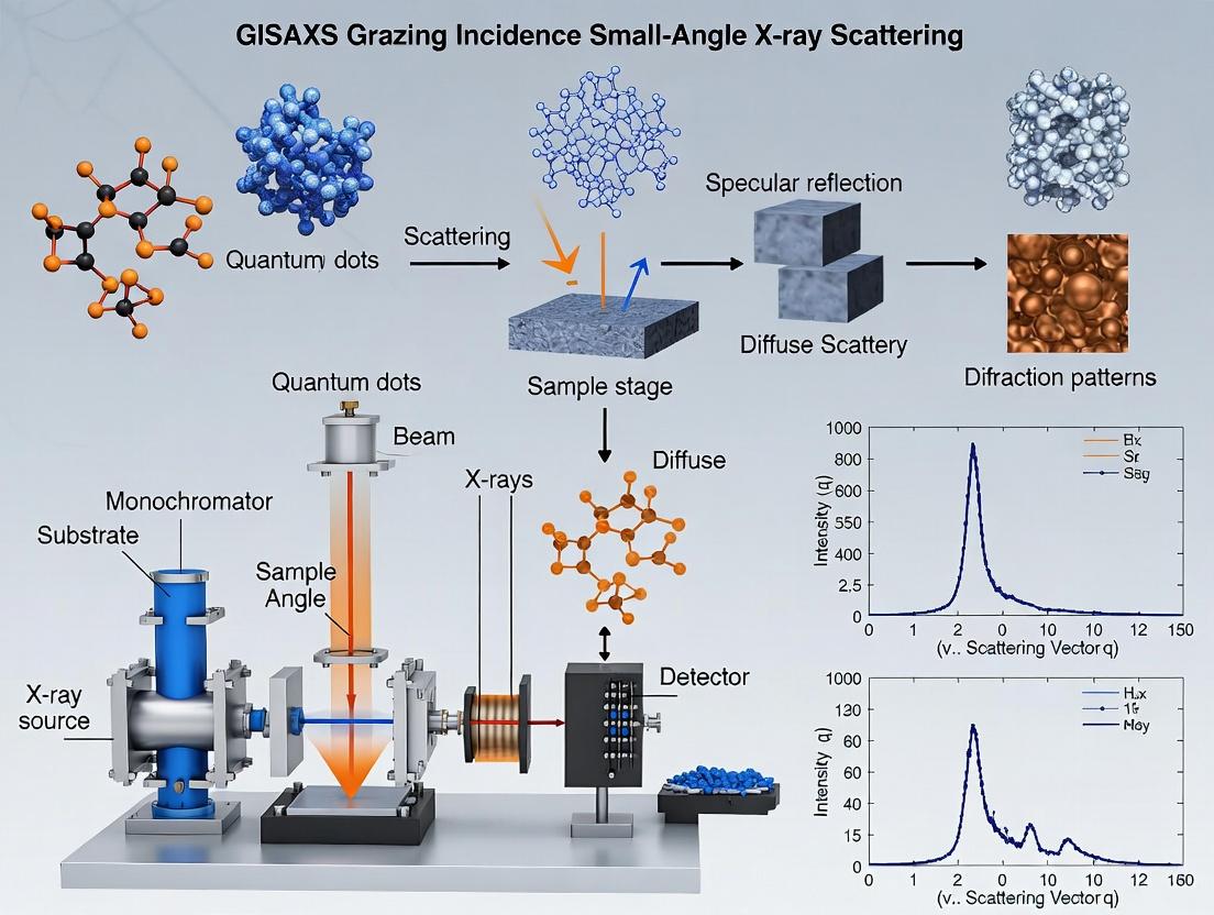
The GISAXS experiment is defined by its unique geometry. An X-ray beam strikes a flat sample at a grazing incidence angle (αi), typically close to or between the critical angles of the substrate and the film material (0.1° - 1.0°). This geometry confines the X-ray wavefield within the surface layer, enhancing sensitivity to near-surface nanostructures. The scattered intensity is recorded on a 2D detector, producing a pattern that is a function of the exit angle (αf) and the in-plane scattering angle (2Θf).
The scattering vector q is decomposed into three components:
- q_z: Out-of-plane component, sensitive to vertical shape, film thickness, and layering.
- q_y: In-plane component, sensitive to lateral ordering, spacing, and shape.
- q_x: Component along the beam direction, often integrated due to the small incidence angle.
Diagram Title: GISAXS Experimental Geometry and Scattering Vector
Application to Quantum Dots and Nanocrystals
For semiconductor QD research, GISAXS provides critical ensemble information complementary to local probes like TEM. Key measurables include:
- Mean Size & Size Distribution: From the radius of gyration analysis of the scattering form factor.
- Shape & Aspect Ratio: Deduced from the anisotropic shape of the 2D scattering pattern.
- In-Plane Ordering & Spatial Correlation: Analyzed from the position and shape of Bragg sheets or correlation peaks along q_y.
- Vertical Position & Embedding Depth: Probed via interference fringes (Yoneda band) and q_z oscillations.
- Particle Density & Layer Thickness: Obtained from the integrated scattering intensity and critical angle measurements.
Table 1: Typical GISAXS Parameters for Quantum Dot Studies
| Parameter | Typical Range for QDs | Information Gained |
|---|---|---|
| Incident Angle (α_i) | 0.1° - 0.5° (Near critical angle) | Enhances surface/interface sensitivity |
| X-ray Wavelength (λ) | 0.5 - 1.5 Å (Synchrotron) | Optimizes q-range and penetration |
| q_y range | 0.001 - 1 nm⁻¹ | Lateral distances from ~6 nm to 6 μm |
| q_z range | 0.1 - 5 nm⁻¹ | Vertical distances from ~1 to 60 nm |
| Measurement Time | 0.1 - 10 seconds (Synchrotron) | Balance of signal-to-noise and throughput |
Experimental Protocols
Protocol: GISAXS Measurement of Self-Assembled Quantum Dot Arrays
Objective: Determine the mean center-to-center distance, size distribution, and lateral order of epitaxially grown InAs QDs on a GaAs substrate.
Materials & Sample Prep:
- Sample: Epitaxial wafer with InAs QDs.
- Substrate cleaving or mounting to ensure a flat, uncontaminated surface.
- Sample holder compatible with ultra-high vacuum or inert gas environments if needed.
Procedure:
- Alignment: Mount sample on a 6-circle goniometer. Use a laser or direct beam to coarsely align the sample surface.
- Critical Angle Determination: Perform an angular reflectivity (XRR) scan at low angles (0° - 2°) to find the critical angles of the substrate and QD layer.
- Incidence Angle Selection: Set α_i to a value slightly above the critical angle of the substrate (e.g., 0.2° - 0.3°) to achieve optimal penetration and scattering volume.
- Beam Definition: Use slits or collimating optics to define a beam footprint of ~10 mm x 0.1 mm on the sample.
- Exposure: Open the detector shutter for a calibrated exposure time (e.g., 1-5 sec at a synchrotron). Ensure the scattering pattern is not saturated.
- Data Collection: Collect 2D scattering images at the chosen αi. Optionally, collect a rocking curve (vary αi slightly) to average over substrate curvature.
- Background Subtraction: Collect and subtract an image with the beam blocked or from a bare substrate.
- Data Reduction: Correct image for detector sensitivity, spatial distortion, and solid angle.
Diagram Title: GISAXS Experimental Workflow for QD Arrays
Protocol: In-Situ GISAXS of Nanocrystal Film Formation
Objective: Monitor the self-assembly and solvent drying kinetics of colloidal PbS nanocrystals during spin-coating.
Materials & Sample Prep:
- Nanocrystal Solution: PbS QDs in toluene (e.g., 20 mg/mL).
- Substrate: Silicon wafer with native oxide, cleaned.
- Spin Coater: Integrated into the GISAXS sample stage or compatible with in-situ cell.
Procedure:
- Initial Setup: Align the clean, dry substrate in the beam. Take a reference GISAXS image.
- Solution Deposition: Rapidly deposit a droplet (~50 µL) of the QD solution onto the static substrate.
- Trigger Acquisition: Immediately start a fast, time-resolved GISAXS measurement sequence (frame rate: 10-100 ms).
- Initiate Spin-Coating: After a short pre-spin delay (<1s), initiate substrate rotation (e.g., 1000-3000 rpm).
- Monitor Evolution: Record the continuous evolution of the 2D pattern through the fluid stage, sol-gel transition, and final dry film formation.
- Final Measurement: Continue measurement until the pattern stabilizes (dry film).
- Data Analysis: Track changes in peak positions (qy for spacing, qz for thickness), intensity, and shape as a function of time.
The Scientist's Toolkit: Key Research Reagent Solutions
Table 2: Essential Materials for GISAXS Studies of Quantum Dots
| Item | Function in GISAXS Experiment |
|---|---|
| High-Brilliance X-ray Source (Synchrotron Beamline) | Provides intense, collimated, and tunable X-rays necessary for probing weak scattering from nanoscale objects with high temporal and spatial resolution. |
| 2D Area Detector (Pixel Array, CCD, or Eiger detector) | Captures the full 2D scattering pattern simultaneously, allowing analysis of anisotropic features and fast kinetics. |
| High-Precision Goniometer (6-circle or custom) | Enables precise alignment of the sample at grazing incidence and allows rocking scans for data averaging. |
| Collimating Optics (Slits, Gobel Mirrors, Compound Refractive Lenses) | Defines and shapes the X-ray beam to achieve a clean, small footprint on the sample, reducing parasitic scattering. |
| Environmental Cell (Vacuum chamber, humidity/temperature control) | Allows control of sample environment (inert gas, vacuum, humidity) for in-situ/operando studies of film processing or device operation. |
| Standard Reference Samples (Polystyrene beads on Si, gratings) | Used for instrument calibration, determining beam center, detector distance, and q-range calibration. |
| Data Analysis Software (Igor Pro with Nika/DPDAK, SAXS utilities, FitGISAXS) | Essential for reducing 2D data, correcting distortions, and performing quantitative modeling and fitting to extract physical parameters. |
Within the broader thesis of utilizing Grazing-Incidence Small-Angle X-ray Scattering (GISAXS) for nanostructured materials research, this whitepaper establishes its unparalleled utility for investigating quantum dots (QDs) and semiconductor nanocrystals. These materials often exhibit mesoscopic order within seemingly disordered ensembles—a paradigm GISAXS is exquisitely designed to probe. This document provides a technical guide on the principles, protocols, and applications of GISAXS for researchers and scientists elucidating the structure-property relationships in nanocrystal systems.
Quantum dots and colloidal nanocrystals are frequently deposited as thin films or assemblies on substrates for applications in photovoltaics, LEDs, and sensors. While these ensembles may appear disordered macroscopically, they often possess short-range order, local packing geometries, and correlation distances critical to electronic and optical properties. Traditional microscopy techniques (TEM, SEM) offer localized real-space images but struggle with statistical representation and subsurface analysis. GISAXS, by contrast, provides a statistically robust, non-destructive probe of in-plane and out-of-plane nanostructure across a large sample area.
Core Principles of GISAXS for Nanocrystal Analysis
GISAXS combines the surface sensitivity of grazing incidence with the statistical power of X-ray scattering. The key measurable parameters for QD/nanocrystal analysis include:
- In-plane ordering: Derived from the azimuthal dependence of Bragg rods or interference fringes.
- Particle size & shape: Determined from the form factor scattering in the qy direction.
- Inter-particle distances & lattice parameters: Extracted from the position of correlation peaks in the qxy direction.
- Film thickness & layer order: Inferred from Kiessig fringes and vertical electron density profiles.
- Orientation & alignment: Assessed from the anisotropy of the scattering pattern.
Quantifiable Outputs and Their Significance
Table 1: Key GISAXS-Derived Parameters for Quantum Dot Characterization
| Parameter | Extracted From | Typical Range for QDs | Physical Significance |
|---|---|---|---|
| Mean Particle Radius (R) | Form factor Guinier region | 1 – 10 nm | Determines quantum confinement, bandgap. |
| Size Dispersity (σ/R) | Form factor decay | 3 – 15% | Impacts emission linewidth, transport uniformity. |
| In-Plane Center-to-Center Distance (d) | Correlation peak qxy | 5 – 20 nm | Defines electronic coupling and charge transport. |
| Paracrystal Disorder Factor (g) | Peak width analysis | 0.05 – 0.3 | Measures lattice disorder; affects mobility. |
| Vertical Correlation Length | Bragg rod length in qz | 1 – 10 particle layers | Indicates epitaxial order or stratified deposition. |
Experimental Protocols for GISAXS on QD Films
Sample Preparation
Objective: Deposit a uniform monolayer or thin film of nanocrystals on a flat, low-roughness substrate (e.g., silicon wafer, glass with Pt/Ir coating).
- Method (Spin-Coating):
- Clean substrate via ultrasonic bath in acetone and isopropanol, followed by oxygen plasma treatment.
- Prepare QD solution in a non-polar solvent (e.g., octane, toluene) at optimized concentration (typically 10-50 mg/mL).
- Dispense solution onto static substrate, then spin at 1500-3000 rpm for 30-60 seconds.
- Optionally, apply a ligand exchange treatment (e.g., with 1,2-ethanedithiol or metal halides) by dipping or spin-coating a second solution to modify inter-dot spacing and coupling.
- Method (Langmuir-Blodgett): For highly ordered monolayers, spread QDs at the air-water interface, compress with barriers to desired surface pressure, and vertically/laterally transfer onto substrate.
GISAXS Measurement Configuration
- X-ray Source: Synchrotron beamline (ideal) or high-brilliance laboratory source (e.g., Ga Kα metaljet).
- Incidence Angle (αi): Set slightly above the critical angle of the substrate (e.g., 0.2° - 0.5° for Si) to achieve full penetration through the QD film while maintaining surface sensitivity.
- Beam Size: 50 x 200 μm (V x H) typical for synchrotron.
- Detector: 2D pixel detector (Pilatus, Eiger) placed 1-5 meters from sample.
- Exposure Time: 0.1 - 10 seconds (synchrotron); 10 minutes - hours (lab source).
Data Reduction and Analysis Workflow
- Correction: Subtract background scattering, correct for detector sensitivity, and mask beamstop shadow.
- Coordinate Transformation: Convert detector pixel coordinates to reciprocal space coordinates (qy, qz).
- Form Factor Modeling: Fit slices along qy at constant qz to a sphere or truncated sphere model to extract core size and dispersity.
- Structure Factor Modeling: Analyze correlation peaks using the Distorted Wave Born Approximation (DWBA) and paracrystal models to extract inter-dot distance and disorder.
Diagram Title: GISAXS Data Analysis Workflow for QDs
The Scientist's Toolkit: Essential Research Reagents & Materials
Table 2: Key Reagent Solutions for QD GISAXS Sample Preparation
| Item / Reagent | Function / Role | Example & Notes |
|---|---|---|
| High-Purity Nanocrystals | Core sample material. Defined size/shape dictates scattering form factor. | PbS, CdSe, CsPbBr3 QDs. Size dispersity <8% is ideal. |
| Anhydrous, Non-Polar Solvents | Dispersing medium for spin-coating; prevents aggregation. | Octane, Toluene, Chloroform. Anhydrous grade preserves ligand integrity. |
| Ligand Exchange Solutions | Modifies surface chemistry and inter-particle spacing. | 1,2-ethanedithiol (EDT) in acetonitrile, Tetrabutylammonium iodide (TBAI) in methanol. |
| Flat, Low-Roughness Substrates | Provides a defined interface for grazing incidence. | Silicon wafers (native oxide), Glass coated with Pt/Ir (for better adhesion). |
| Plasma Cleaner | Creates a hydrophilic, contaminant-free surface for uniform wetting. | Oxygen or argon plasma. Critical for reproducible film formation. |
| Langmuir-Blodgett Trough | For assembling highly ordered QD monolayers. | Controls surface pressure during deposition. |
Advanced Analysis: Decoupling Form & Structure
The power of GISAXS lies in separating the form factor (particle shape) from the structure factor (particle arrangement). For core-shell QDs, the form factor reveals core and shell dimensions. The structure factor, often modeled using a 2D paracrystal lattice, quantifies the degree of translational order.
Diagram Title: Decoupling Form and Structure Factors
Case Study & Quantitative Data
Recent research on CsPbI3 perovskite nanocrystal films for LEDs demonstrates GISAXS's capability. Analysis of films treated with different ligands revealed clear correlations between structural order and device performance.
Table 3: GISAXS-Derived Structural Parameters vs. Device Performance for CsPbI3 QD Films
| Ligand Treatment | Mean Center-to-Center Distance (d, nm) | Paracrystal Disorder (g) | Photoluminescence Quantum Yield (%) | LED EQE (%) |
|---|---|---|---|---|
| Oleic Acid / Oleylamine (OA/OAm) | 8.2 ± 0.5 | 0.28 | 45 | 1.2 |
| Short-Chain Iodide (NaI) | 6.5 ± 0.3 | 0.15 | 78 | 8.5 |
| Bidentate (EDT) | 5.8 ± 0.2 | 0.09 | 92 | 12.7 |
The data quantitatively shows how ligand-induced closer packing (decreased d) and improved order (decreased g) directly enhance optical and electronic performance.
As argued in this thesis, GISAXS is not merely a complementary technique but a foundational tool for advancing quantum dot and nanocrystal science. It uniquely quantifies the hidden structural order in disordered systems, providing the essential link between nanoscale synthesis, mesoscale assembly, and macroscopic device performance. Its non-destructive, statistical nature makes it indispensable for researchers and developers optimizing next-generation nanomaterials.
This technical guide details the core parameters extracted from Grazing-Incidence Small-Angle X-ray Scattering (GISAXS) experiments applied to quantum dots (QDs) and semiconductor nanocrystals. Within the broader thesis of advanced nanostructure characterization, GISAXS emerges as a non-destructive, statistical technique capable of probing the in-plane and out-of-plane structure of nanostructured films and assemblies. It is indispensable for correlating synthetic and processing conditions with the resultant structural order, which directly governs the optoelectronic properties of devices such as QD solar cells, LEDs, and single-photon sources.
Core Parameters: Definition and Physical Significance
Size and Shape
- Definition: The nanoscale dimensions (radius, edge length) and geometric form (sphere, cube, rod, pyramid) of individual nanocrystals.
- Significance: Size determines quantum confinement effects (bandgap tuning). Shape influences faceting, surface energy, and dipole moments. GISAXS distinguishes shapes via the form factor scattering signature.
Inter-particle Distance
- Definition: The mean center-to-center separation between neighboring nanocrystals within an ensemble or a superlattice.
- Significance: Dictates the strength of electronic coupling (e.g., Forster Resonance Energy Transfer, charge transport). Controlled by ligand length, solvent evaporation rate, and inter-particle forces.
Lateral Ordering
- Definition: The degree of spatial periodicity and symmetry in the arrangement of nanocrystals parallel to the substrate (e.g., hexagonal, square, or disordered packing).
- Significance: Long-range order is critical for creating functional metamaterials and engineered band structures. Defect density influences charge transport uniformity.
Experimental Protocols for GISAXS on Nanocrystals
Protocol 1: Sample Preparation for Drop-Cast Films
- Nanocrystal Synthesis: Synthesize monodisperse QDs (e.g., PbS, CdSe) via hot-injection methods.
- Purification: Precipitate QDs using a polar antisolvent (e.g., ethanol/acetone for hydrophobic QDs), centrifuge (10,000 rpm, 10 min), and redisperse in a non-polar solvent (toluene, octane). Repeat 3 times.
- Substrate Cleaning: Sonicate silicon wafer (with native oxide) or glass substrate sequentially in acetone, isopropanol, and deionized water for 15 minutes each. Treat with UV-Ozone for 20 minutes.
- Film Deposition: Pipette 10-50 µL of QD solution (concentration 5-20 mg/mL) onto the static, leveled substrate. Allow slow evaporation in a Petri dish covered loosely to control dust.
Protocol 2: Synchrotron GISAXS Measurement
- Alignment: Mount sample on a high-precision goniometer. Align the sample surface to the incident X-ray beam (~10 keV, λ ~ 0.1 nm) with micrometer accuracy.
- Angle Setting: Set the incident angle (αi) to 0.1° - 0.5°, just above the critical angle of the substrate for total external reflection, to create an evanescent wave and enhance surface sensitivity.
- Data Acquisition: Use a 2D pixelated detector (e.g., Pilatus 2M) placed ~2-5 m downstream. Acquire scattering patterns with exposure times of 0.1-10 seconds, ensuring no detector saturation.
- Beamline Examples: Advanced Photon Source (12-ID-B), ESRF (ID10), PETRA III (P03).
Protocol 3: In-Situ GISAXS During Solvent Annealing
- Chamber Setup: Place the drop-cast QD film in a hermetically sealed chamber with Kapton windows for X-ray transmission.
- Solvent Vapor Introduction: Introduce a controlled flow of solvent vapor (e.g., hexane, dichloroethane) using mass flow controllers to raise the vapor pressure to 20-80% of the saturation vapor pressure.
- Real-Time Monitoring: Continuously acquire GISAXS patterns (0.5-5 sec/frame) as the solvent vapor swells the ligand shell, increasing nanocrystal mobility and promoting reorganization.
- Data Workup: Subtract background scattering (empty chamber). Use radial/azimuthal integration to monitor the evolution of peak position (inter-distance) and peak width (order) over time.
Data Presentation: Quantitative Parameters from Recent Studies
Table 1: GISAXS-Derived Structural Parameters from Select Recent Studies (2023-2024)
| Nanocrystal System | Core Size (nm) [Shape] | Inter-particle Distance (nm) | Lateral Ordering (Symmetry, Paracrystal Disorder %) | Key Finding | Ref. |
|---|---|---|---|---|---|
| CsPbBr3 Perovskite QDs | 8.2 ± 0.5 [Cube] | 9.8 ± 0.3 | BCC (Body-Centered Cubic), 8% | Ligand-assisted superlattice assembly shows enhanced coupling. | ACS Nano (2024) |
| PbS QDs (IR-active) | 3.5 ± 0.2 [Sphere] | 5.1 (EDT-linked) | Disordered, N/A | Short bifunctional ligands reduce inter-dot distance, boosting conductivity. | Adv. Mater. (2023) |
| Fe3O4 Nanocubes | 12.0 ± 0.6 [Cube] | 15.2 ± 0.5 | 2D Hexagonal, 5% | Substrate patterning directs large-area (mm²) superlattice formation. | Nature Comm. (2023) |
| Au Nanospheres | 7.8 ± 0.4 [Sphere] | 10.5 ± 0.4 | FCC (Face-Centered Cubic), 4% | In-situ GISAXS reveals a two-stage crystallization mechanism during evaporation. | Nano Lett. (2024) |
The Scientist's Toolkit: Essential Research Reagents & Materials
Table 2: Key Research Reagent Solutions for QD GISAXS Samples
| Item | Function/Description | Example (Vendor) |
|---|---|---|
| High-Purity Solvents | For synthesis, purification, and film deposition. Low residue is critical for clean superlattice formation. | Anhydrous Toluene (99.8%, Sigma-Aldrich), n-Octane (99%, Alfa Aesar) |
| Ligand Solutions | Used for post-synthetic ligand exchange to modify inter-particle spacing and surface chemistry. | 1,2-Ethanedithiol (EDT, 95%) in Acetonitrile, Oleic Acid in Hexane. |
| Precision Substrates | Flat, low-roughness substrates minimize background scattering. | Single-side polished Si wafers (University Wafer), Fused Silica slides (ESCO). |
| Calibration Standards | Used to calibrate the q-scale of the GISAXS detector. | Silver Behenate powder (for small-angle), Crystalline Si (for wide-angle). |
| Sample Environment Cells | For in-situ studies (annealing, drying, ligand exchange). | Humidity/Temperature controlled stage (Linkam), Gas/Vapor flow cell. |
Visualization: GISAXS Workflow and Data Analysis Logic
Title: GISAXS Experiment and Analysis Workflow for QDs
Title: GISAXS Pattern Features to Parameter Extraction
Within the research paradigm of quantum dots (QDs) and semiconductor nanocrystals, achieving precise control over size, shape, assembly, and superlattice order is paramount for optoelectronic applications. Grazing-Incidence Small-Angle X-ray Scattering (GISAXS) has emerged as a critical, non-destructive in situ probe for these nanostructures. This whitepaper decodes the core features of a GISAXS pattern—Yoneda wings, Bragg rods, and the interplay of form and structure factors—framed within the thesis that quantitative GISAXS modeling is essential for correlating synthetic parameters of colloidal nanocrystals with their mesoscale ordering and interfacial morphology in thin films.
Core Concepts Decoded
The Yoneda Wing: An Interface-Sensitive Feature
The Yoneda wing is a diffuse scattering maximum occurring at the critical angle of the substrate or film material. It arises from enhanced scattering when the incident or exit angle matches the critical angle for total external reflection, maximizing the X-ray electric field intensity at the interface.
Primary Information Content:
- Sensitive probe of interfacial roughness and lateral correlation lengths at the substrate/film or film/air interface.
- Critical for analyzing wetting layers, initial nucleation density, and island formation in QD films.
Quantitative Data Summary: Table 1: Yoneda Wing Parameters and Physical Significance
| Parameter | Typical Range (for Si substrate) | Physical Property Probed | Relevance to QD Films |
|---|---|---|---|
| Yoneda Position (αf / 2θf) | ~0.22° (for Si, λ=0.154 nm) | Material critical angle (electron density) | Identifies scattering from substrate, QD layer, or capping layer. |
| Wing Width (Δq_y) | 0.01 - 0.5 nm⁻¹ | Lateral correlation length (ξ) via ξ ≈ 2π/Δq_y | Nuclei or island separation early in deposition. |
| Wing Intensity Profile | — | Interfacial roughness and cross-correlation. | Evolution of film smoothness/coverage during solvent annealing. |
Bragg Rods: Signatures of 3D Order
Bragg rods are extended streaks of scattering along the out-of-plane (q_z) direction arising from Bragg diffraction by a crystalline lattice with finite thickness or disorder along the surface normal. In GISAXS, they indicate the presence of long-range in-plane order but limited out-of-plane coherence.
Primary Information Content:
- Confirms the formation of a 3D ordered nanocrystal superlattice.
- The rod position in q_y gives in-plane lattice spacing.
- The modulation and decay along q_z provide out-of-plane stacking order, number of layers, and interlayer spacing.
Experimental Protocol for Analyzing Superlattice Order:
- Sample Preparation: Deposit colloidal PbS or CsPbBr₃ QDs via drop-casting or spin-coating onto a Si wafer. Apply controlled solvent vapor annealing to promote self-assembly.
- GISAXS Measurement: Use a synchrotron beam (λ ≈ 0.1 nm) at a grazing incidence angle (α_i > substrate critical angle). Use a 2D detector.
- Data Reduction: Correct for detector geometry, flood field, and incident angle. Perform azimuthal integration around the Bragg rod to obtain intensity vs. q_xy profiles.
- Modeling: Fit the qxy peaks to a paracrystalline model (using e.g., IsGISAXS software or BornAgain) to extract lattice parameter, domain size, and disorder factor (σd/d).
Form Factor (F) vs. Structure Factor (S): Disentangling Shape from Order
The GISAXS intensity is fundamentally governed by: I(q) ∝ |F(q)|² · S(q), where:
- Form Factor |F(q)|²: Scattering from an individual nanoparticle. Encodes its size, shape (sphere, cube, rod), and internal electron density contrast.
- Structure Factor S(q): Interference between waves scattered from different nanoparticles. Encodes the spatial arrangement (liquid-like, hexagonal, cubic order) and interparticle distances.
Decoding Strategy for Core/Shell QDs:
- Isolate |F|² by measuring a highly dilute, disordered monolayer (where S(q)≈1).
- Model |F|² using shapes (e.g., sphere, truncated cube) to determine core size and shape dispersion.
- Isolate S(q) by analyzing the intensity modulation of Bragg peaks from a concentrated superstructure, using the previously determined |F|².
- Extract superlattice symmetry, lattice constant, and paracrystalline disorder.
Visualization of the GISAXS Analysis Workflow
Title: GISAXS Analysis Pipeline for Quantum Dot Films
The Scientist's Toolkit: Essential Research Reagents & Materials
Table 2: Key Research Reagent Solutions for GISAXS Studies of Nanocrystals
| Item | Function in GISAXS Research |
|---|---|
| Monodisperse Colloidal Nanocrystals (e.g., PbS, CdSe, CsPbBr₃) | The core research material. Size/shape dispersion defines form factor. Surface ligands dictate self-assembly and structure factor. |
| Functionalized Silicon Wafers (with native or thermal oxide) | Standard substrate. Low roughness, well-defined critical angle for Yoneda analysis. Can be functionalized with polymers/ligands to control wetting. |
| Solvent Vapor Annealing (SVA) Chamber | Controlled environment to promote nanocrystal mobility and superlattice formation in situ during GISAXS measurement. |
| Precision Syringe & Spin Coater | For reproducible deposition of nanocrystal solutions into uniform thin films. |
| GISAXS Simulation Software (BornAgain, IsGISAXS, FitGISAXS) | Essential for modeling form/structure factors via Distorted Wave Born Approximation (DWBA) to extract quantitative parameters. |
| Synchrotron Beamtime (or high-flux lab-source) | High photon flux is required to obtain statistically meaningful scattering from dilute nanoscale objects in short timeframes, especially for in situ studies. |
Within the broader thesis on Grazing-Incidence Small-Angle X-ray Scattering (GISAXS) for Studying Quantum Dots and Semiconductor Nanocrystals, the choice of X-ray source is a fundamental, equipment-driven decision. This guide provides a technical comparison between synchrotron and lab-based sources, detailing their impact on experimental protocols, data quality, and research outcomes in nanocrystal film characterization.
Quantitative Comparison: Source Characteristics
Table 1: Core Performance Metrics of X-ray Sources for GISAXS
| Parameter | Synchrotron Beamline (e.g., Advanced Photon Source) | Lab-Based Source (Rotating Anode, Cu Kα) | Lab-Based Source (Metal Jet, Ga Kα) |
|---|---|---|---|
| Photon Energy | Tunable, typically 5-20 keV | Fixed, 8.04 keV (Cu Kα) | Fixed, 9.24 keV (Ga Kα) |
| Beam Flux (photons/s) | 10^12 – 10^15 | 10^8 – 10^9 | 10^9 – 10^10 |
| Beam Divergence (mrad) | < 0.01 | ~ 0.5 – 1.0 | ~ 0.3 – 0.8 |
| Beam Size (μm) | 10 – 100 (easily focused) | 50 – 500 | 30 – 200 |
| Typical GISAXS Measurement Time | 0.01 – 1 second | 10 minutes – several hours | 1 – 30 minutes |
| Access Mode | Proposal-based, scheduled beam time | In-house, on-demand | In-house, on-demand |
| Anisotropy/Resonant Scattering | Yes (tunable energy) | No | No |
Table 2: GISAXS Data Quality & Applicability for Nanocrystals
| Aspect | Synchrotron-Based GISAXS | Lab-Based GISAXS |
|---|---|---|
| Q-range & Resolution | Wide, high-resolution; detects weak features. | Limited; suitable for strong scatterers and larger structures. |
| Time-Resolved Studies | Millisecond to second dynamics (e.g., annealing, ligand exchange). | Minutes to hours; static or very slow processes. |
| Sample Throughput | Extremely high for screening. | Low to moderate. |
| Signal-to-Noise Ratio | Excellent, even for ultrathin films or dilute nanocrystal arrays. | Moderate; requires optimized samples with strong scattering. |
| Primary Research Context | High-precision structure, in-situ/operando dynamics, anomalous GISAXS. | Routine characterization, batch-to-batch variation, initial film optimization. |
Experimental Protocols for GISAXS on Nanocrystal Films
Protocol 1: Synchrotron GISAXS for In-Situ Thermal Annealing
- Objective: Study the real-time evolution of nanocrystal superlattice order and spacing during thermal processing.
- Sample Preparation: Spin-coat nanocrystal (e.g., PbS QD) solution onto a cleaned silicon substrate in a nitrogen glovebox. Load onto a heating stage in a vacuum-compatible chamber.
- Beamline Setup:
- Select energy (e.g., 10 keV) using a double-crystal monochromator.
- Define beam size (50 x 50 μm) with Kirkpatrick-Baez mirrors.
- Set grazing incidence angle (~0.2°) above the substrate critical angle.
- Data Acquisition:
- Align sample and detector (2D area detector, e.g., Pilatus).
- Begin temperature ramp (e.g., 25°C to 150°C at 5°C/min).
- Acquire consecutive GISAXS frames with 100 ms exposure per frame.
- Data Reduction: Use SAXS software (e.g., SAXSGUI, DAWN) for radial integration, correction for background, and incident flux.
Protocol 2: Lab-Based GISAXS for Ligand Shell Thickness Determination
- Objective: Determine average core size and ligand shell thickness of oleic acid-capped CdSe nanocrystals in a dried film.
- Sample Preparation: Drop-cast concentrated nanocrystal solution onto a Si wafer, allowing slow evaporation for self-assembly.
- Source Setup: Align a Ga Kα (9.24 keV) sealed tube or metal-jet source with a multilayer optic. Use motorized slits to define a 200 x 200 μm beam.
- Data Acquisition:
- Pre-align sample stage using a laser and camera.
- Optimize the incidence angle via detector count rate.
- Acquire a single 2D GISAXS pattern with a 30-minute exposure using a hybrid pixel detector (e.g., Eiger2 R 1M).
- Data Analysis: Fit the radially averaged 1D scattering profile with a form factor model (e.g., spherical core-shell) accounting for paracrystalline disorder.
Visualization: GISAXS Workflow & Decision Logic
Title: GISAXS Source Selection Decision Tree
Title: Core GISAXS Experimental Workflow
The Scientist's Toolkit: Key Research Reagent Solutions
Table 3: Essential Materials for Nanocrystal GISAXS Sample Preparation
| Item | Function in GISAXS Research |
|---|---|
| High-Purity Semiconductor Precursors (e.g., CdO, PbO, Trioctylphosphine Selenide) | Synthesis of monodisperse quantum dots with controlled core size, the primary scatterer. |
| Ligands (e.g., Oleic Acid, Oleylamine, Short-chain Carboxylic Acids) | Control nanocrystal surface chemistry, inter-dot spacing in the film, and self-assembly behavior. |
| Anhydrous, Oxygen-Free Solvents (e.g., Octadecene, Toluene in sealed bottles) | For synthesis and film processing to prevent oxidation and degradation of nanocrystal surfaces. |
| Atomically Flat Substrates (e.g., Prime-grade Si wafers, float-glass) | Provide a smooth, low-scattering background for grazing incidence geometry. |
| Substrate Cleaning Solutions (Piranha solution, UV-Ozone cleaner) | Ensure pristine, hydrophilic surfaces for uniform nanocrystal film deposition. |
| Spin Coater or Langmuir-Blodgett Trough | Tools for creating large-area, uniform thin films of nanocrystals with controlled thickness. |
| Inert Atmosphere Glovebox | Essential environment for all sample preparation steps to maintain nanocrystal surface integrity before measurement. |
Step-by-Step GISAXS Protocols for Quantum Dot Films and Biomedical Assemblies
This technical guide details critical sample preparation methodologies within the broader thesis context of employing Grazing-Incidence Small-Angle X-ray Scattering (GISAXS) for the structural investigation of quantum dots (QDs) and semiconductor nanocrystals. The quality and reproducibility of GISAXS data are fundamentally dependent on the precise engineering of the sample substrate, the controlled deposition of nanomaterials, and the assurance of sample stability throughout measurement.
Substrate Selection and Preparation
The substrate serves as the foundation for GISAXS experiments, influencing nanocrystal dispersion, ordering, and signal-to-noise ratio.
Substrate Types and Properties
| Substrate Type | Material | Typical RMS Roughness | Primary Advantage | Ideal For |
|---|---|---|---|---|
| Silicon Wafer | Si with native SiO₂ | < 0.5 nm | Ultra-smooth, excellent for GISAXS | Thin films, self-assembled monolayers |
| Glass (Microscope Slide) | Borosilicate | ~ 1 nm | Low-cost, optically transparent | Pilot studies, optical correlation |
| Mica | Muscovite | Atomically flat upon cleavage | Atomically flat, cleavable | Fundamental studies of ordering |
| Fused Silica | SiO₂ | < 1 nm | Low background scattering, UV-transparent | In-situ/operando studies with optical excitation |
| Polymer Films | PMMA, PS | Variable, can be high | Flexible, tunable surface energy | Printable electronics, flexible devices |
Substrate Cleaning Protocols
Protocol for Silicon Wafer Cleaning (RCA Standard Clean):
- Solvent Clean: Sonicate in acetone for 10 minutes, followed by isopropanol for 10 minutes. Dry with N₂.
- RCA-1 (Organic Removal): Prepare a 5:1:1 mixture of H₂O (deionized), NH₄OH (28-30%), and H₂O₂ (30%). Heat to 70-80°C. Immerse substrates for 10-15 minutes. Rinse thoroughly with DI water.
- RCA-2 (Ionic Removal): Prepare a 5:1:1 mixture of H₂O (deionized), HCl (37%), and H₂O₂ (30%). Heat to 70-80°C. Immerse substrates for 10-15 minutes.
- Final Rinse & Dry: Rinse copiously with DI water (18.2 MΩ·cm) and dry under a stream of N₂. Store in a clean container.
Protocol for Oxygen Plasma Treatment:
- Purpose: Increases surface hydrophilicity by generating -OH groups, essential for uniform aqueous solution deposition.
- Parameters: Use a plasma cleaner at medium RF power (50-100W). Expose substrates to O₂ plasma for 30-120 seconds. Use within 30 minutes of treatment for optimal results.
Deposition Techniques
The method of depositing QD/nanocrystal dispersions onto the substrate controls film morphology, thickness, and homogeneity.
Common Techniques and Outcomes
| Technique | Typical Film Thickness Range | Uniformity Control | Key Parameter | Throughput |
|---|---|---|---|---|
| Spin-Coating | 10 nm - 1 μm | High (center to edge) | Spin speed (rpm), acceleration, time | High |
| Drop-Casting | 100 nm - 10 μm (non-uniform) | Low | Solvent volatility, concentration | High |
| Dip-Coating | 10 nm - 200 nm per layer | Moderate | Withdrawal speed, immersion time | Moderate |
| Langmuir-Blodgett | 1 monolayer (precise) | Very High | Surface pressure, compression speed | Low |
| Inkjet Printing | 50 nm - 5 μm (patterned) | High within droplet | Ink viscosity, drop spacing, substrate temperature | Moderate |
Detailed Spin-Coating Protocol for Core/Shell QDs
Objective: Produce a uniform, closed monolayer or thin film of oleic-acid capped PbS/CdS QDs for GISAXS analysis of inter-dot spacing and film order.
- QD Ink Preparation: Dilute the stock QD solution in anhydrous octane to a concentration of 15-25 mg/mL. Filter through a 0.2 μm PTFE syringe filter.
- Substrate Preparation: Use an RCA-cleaned, O₂-plasma-treated silicon wafer. Mount on the spin coater chuck.
- Deposition: Pipette 50-100 μL of the QD ink onto the stationary substrate.
- Spinning: Execute a two-step program: (i) 500 rpm for 5 seconds (spread stage), (ii) 1500-2000 rpm for 30 seconds (thin film stage).
- Post-Processing: Immediately anneal the film on a hotplate at 80°C for 5 minutes to remove residual solvent. For ligand exchange, immerse in a solution of 1% ethanedithiol in acetonitrile for 30 seconds, followed by acetonitrile rinse and dry.
Stability Considerations
Sample degradation during measurement or storage can invalidate GISAXS data.
Major Degradation Pathways & Mitigation
- Oxidation (e.g., of PbS QDs): Exposure to air/oxygen leads to broadening of GISAXS peaks. Mitigation: Perform preparation in N₂ glovebox. Use sealed sample cells with Kapton or graphene windows for measurement.
- Ligand Desorption/Decomposition: Alters inter-particle spacing and ordering. Mitigation: Characterize thermal stability via TGA prior to experiment. Use stable bidentate ligands (e.g., alkanedithiols).
- Beam-Induced Damage: High-flux X-ray beams can degrade organic ligands or induce crystallization in amorphous matrices. Mitigation: Use a beam attenuator, reduce exposure time, raster the sample, or use a cryo-cooling stage if applicable.
Stability Assessment Protocol
- Pre- and Post-Measurement Characterization: Record optical absorbance/PL spectra before and after GISAXS run. A spectral shift or quenching indicates degradation.
- Time-Resolved GISAXS: Perform sequential short exposures on the same spot. Plot scattering peak position/intensity vs. time to monitor in-situ stability.
- Controlled Environment: For air-sensitive samples, use an in-vacuum or inert-gas-flow sample stage.
The Scientist's Toolkit: Key Research Reagent Solutions
| Item | Function in QD GISAXS Sample Prep |
|---|---|
| Anhydrous Octane/Toluene | High-purity, low-polarity solvent for dispersing oleophilic QDs; minimizes aggregation during deposition. |
| Ethanedithiol (EDT) / 3-Mercaptopropionic Acid (MPA) | Ligand exchange agents to replace long-chain native ligands, shorten inter-dot distance, and improve charge transport. |
| Ammonium Hydroxide & Hydrogen Peroxide (RCA solutions) | Critical components for removing organic and ionic contaminants from silicon substrates. |
| PTFE Syringe Filter (0.2 μm) | Removes large aggregates and dust from QD inks prior to deposition, ensuring a defect-free film. |
| Oxygen Plasma Cleaner | Modifies substrate surface energy to achieve uniform wetting and film formation. |
| Polydimethylsiloxane (PDMS) Wells | Creates physical barriers on substrates for containing QD solutions during drop-casting or in-situ liquid cell experiments. |
| Lead Acetate Trihydrate & Bis(trimethylsilyl) sulfide (TMS2S) | Common precursors for the synthesis of PbS QDs, the model system for many GISAXS studies. |
| 1-Octadecene & Oleic Acid | Common solvent and capping ligand used in hot-injection QD synthesis, defining initial surface chemistry. |
Experimental Workflow & Signaling Pathways
Diagram Title: GISAXS Sample Preparation and Validation Workflow
Diagram Title: Quantum Dot Film Degradation Pathways and GISAXS Signatures
In Grazing-Incidence Small-Angle X-ray Scattering (GISAXS) studies of quantum dots (QDs) and semiconductor nanocrystals, the incident angle ((αi)) of the X-ray beam relative to the sample surface is the critical parameter governing the trade-off between surface sensitivity and bulk penetration. This guide details the technical considerations and protocols for optimizing (αi) to probe either the near-surface nanostructure or the embedded bulk morphology, a central capability for advancing applications in photovoltaics, quantum computing, and nanomedicine.
GISAXS leverages grazing incidence to enhance scattering signal from nanostructures on or beneath a surface. The choice of (αi) relative to the sample’s critical angle ((αc)) determines the X-ray penetration depth and the evanescent wave field’s decay length. For QD assemblies, superlattices, or nanocrystals embedded in polymer matrices, strategic navigation of this parameter allows selective probing of different sample strata.
Fundamental Principles: Critical Angle and Penetration Depth
Defining Key Parameters
The critical angle (αc) (in radians) is material-dependent: [ αc ≈ λ \sqrt{\frac{re ρ}{π}} ] where (λ) is the X-ray wavelength, (re) is the classical electron radius, and (ρ) is the electron density of the substrate or film.
Penetration Depth Regimes
The penetration depth Λ varies dramatically with (α_i):
| Incident Angle Regime | Relation to (α_c) | Effective Probe Depth | Primary Information Gained |
|---|---|---|---|
| Total External Reflection | (αi < αc) | ~5-10 nm (evanescent wave) | Ultra-surface layer, QD monolayer ordering, top-film morphology. |
| Surface-Sensitive | (αi ≈ αc) | 10-100 nm | Shallow embedded nanocrystals, interfacial mixing, thin-film density gradients. |
| Bulk-Penetrating | (αi > 1.5 \times αc) | Several microns | Deeply embedded QDs, bulk nanocomposite structure, substrate effects. |
Table 1: GISAXS operational regimes defined by incident angle.
Experimental Protocols for Incident Angle Optimization
Protocol: Determining the Critical Angle
- Material: Silicon wafer or thin-film substrate with/without nanocrystal coating.
- Tool: Synchrotron beamline with precise goniometer (angular resolution < 0.001°).
- Procedure: a. Perform an X-ray reflectivity (XRR) scan at very low qz (e.g., 0-0.5° in (αi)). b. Fit the resulting curve to obtain the precise (α_c) for the substrate-film system. c. For composite samples, note the appearance of multiple critical angles from different layers.
Protocol: Angle-Resolved GISAXS Mapping for Stratified Nanocrystal Films
- Sample Preparation: Spin-coat a layered film: e.g., a dense monolayer of PbS QDs atop a PMMA film containing dispersed CdSe nanocrystals.
- Data Acquisition: a. Set detector distance (typically 1-5 m) and calibrate with a standard (e.g., silver behenate). b. Perform a series of GISAXS measurements at incrementally increasing (αi) (e.g., from 0.8(αc) to 3(α_c)). c. For each angle, acquire a 2D scattering pattern with sufficient exposure time (~1-5 s).
- Data Analysis: a. Extract vertical (qz) and horizontal (qy) line cuts from each 2D pattern. b. Analyze changes in diffuse scattering, Yoneda band intensity, and Bragg rod features versus (α_i). c. Model data using the Distorted Wave Born Approximation (DWBA) to deconvolute surface vs. bulk scattering contributions.
Diagram Title: GISAXS Incident Angle Optimization Workflow
The Scientist's Toolkit: Essential Research Reagent Solutions
| Item / Reagent | Function in GISAXS of QDs/Nanocrystals |
|---|---|
| High-Purity Silicon Wafers (P/B doped, <100>) | Standard, low-roughness substrate for precise (α_c) determination and model film studies. |
| Silver Behenate (AgBh) Powder | Calibration standard for q-space (scattering vector) due to its well-defined lamellar spacing. |
| Lead Sulfide (PbS) / Cadmium Selenide (CdSe) Quantum Dots (Octane/Toluene dispersions) | Model colloidal nanocrystal systems with tunable size, composition, and optoelectronic properties. |
| Poly(methyl methacrylate) (PMMA) | Transparent polymer matrix for embedding nanocrystals to create model bulk nanocomposites. |
| 1,2-Ethanedithiol (EDT) / 3-Mercaptopropionic Acid (MPA) | Ligand exchange solutions to alter QD surface chemistry and inter-dot spacing in assemblies. |
| Polydimethylsiloxane (PDMS) Stamps | Used for micro-contact printing to create patterned QD monolayers for GISAXS studies of order. |
Table 2: Key materials for GISAXS experiments on quantum dots and nanocrystals.
Data Interpretation and Modeling
Signal Deconvolution Using DWBA
Scattering intensity (I(q)) in the DWBA framework for (αi) near (αc): [ I(q) ∝ | T(αi)T(αf) |^2 S(q) ] where (T) are the Fresnel transmission coefficients and (S(q)) is the nanostructure form factor. This model is essential for separating the scattering contribution of surface-located QDs from those submerged in the substrate or matrix.
Quantitative Data from Angle-Resolved Studies
Example data from a study on CsPbBr₃ perovskite nanocrystal films:
| Sample Layer | Optimal (αi / αc) | Probed Thickness | Key Extracted Parameter | Value |
|---|---|---|---|---|
| QD Superlattice (Top) | 0.92 | 8 nm | Center-to-center dot spacing | 12.3 ± 0.4 nm |
| Interfacial Mixing Layer | 1.05 | 45 nm | Polymer nanocrystal density | 18 ± 3 vol% |
| Bulk Composite | 2.10 | > 2000 nm | Correlation length of density fluctuations | 152 ± 15 nm |
Table 3: Example structural data extracted from different incident angle regimes.
Advanced Applications: In-Situ and Time-Resolved Studies
Optimizing (α_i) is paramount for in-situ experiments:
- QD Self-Assembly during Solvent Evaporation: Use (αi < αc) to monitor the evolution of the top monolayer.
- Thermal Annealing of Nanocomposites: Use (αi ≈ αc) to track diffusion and sintering at the polymer-air interface.
- Electrochemical Cycling of QD Electrodes: Use (αi > αc) to probe structural changes throughout the bulk electrode during ion insertion/extraction.
Diagram Title: In-Situ GISAXS Strategy for Stimulated QD Films
Mastery of incident angle optimization in GISAXS provides a powerful, non-destructive method for constructing a three-dimensional structural picture of complex quantum dot and nanocrystal systems. By deliberately toggling between surface-sensitive and bulk-penetrating regimes, researchers can resolve open questions regarding interface quality, embedding efficiency, and structural homogeneity—key factors dictating performance in next-generation quantum and semiconductor devices.
Within the broader thesis on Grazing-Incidence Small-Angle X-ray Scattering (GISAXS) for investigating quantum dots (QDs) and semiconductor nanocrystals, this guide focuses on advanced in-situ and operando methodologies. The dynamic study of self-assembly kinetics and thermal processing is critical for tailoring optoelectronic properties in devices such as QD solar cells, LEDs, and nanoscale sensors. This whitepaper provides a technical framework for designing experiments that capture real-time structural evolution under relevant processing conditions.
Core Principles ofIn-SituandOperandoGISAXS
In-situ GISAXS involves conducting measurements while a sample undergoes a controlled process (e.g., heating, solvent annealing). Operando GISAXS extends this concept by measuring under the actual operating conditions of a device (e.g., under applied voltage or illumination), establishing a direct structure-function correlation. For QD films, key parameters accessible via GISAXS include:
- Lateral ordering: Paracrystal lattice parameters, domain size.
- Vertical structure: Layer thickness, interface roughness.
- Shape & Size: Nanocrystal form factor (if resolved).
- Morphology Evolution: Real-time changes during processing.
Experimental Design & Setup Configuration
A successful experiment integrates a specialized sample environment with synchrotron beamline capabilities.
3.1. Essential Hardware Components The setup extends a standard GISAXS instrument with environmental control.
| Component | Function & Specification |
|---|---|
| Micrometric Stage | Precise sample positioning (xyz, tilt). Must be non-magnetic if using EM fields. |
| Environmental Cell | Sealed chamber with X-ray transparent windows (e.g., Kapton, SiN). |
| Precision Heater | For thermal processing. Requires fast feedback control (stability ±0.5°C). |
| UV/Visible Light Source | For operando photoluminescence or photoconditioning studies. |
| Gas Flow System | For controlled atmosphere (inert, reactive) or solvent vapor annealing. |
| 2D X-ray Detector | Fast-readout, low-noise detector (e.g., Pilatus, Eiger). |
3.2. Beamline Considerations
- Beam Energy: Typically 8-18 keV. Higher energy increases penetration for complex cells.
- Beam Size: 50-200 µm. Smaller size enables probing local homogeneity.
- Incidence Angle (αi): Must be slightly above the critical angle of the substrate (≈0.1-0.3°) to probe the film structure, but can be varied to achieve depth sensitivity.
Detailed Methodologies for Key Experiments
4.1. Protocol: In-Situ Thermal Annealing of QD Superlattices Objective: Monitor the ordering and sintering of colloidal QD arrays during temperature ramp.
- Sample Prep: Deposit PbS or CdSe QD film via spin-coating/Langmuir-Blodgett onto Si/SiO₂ substrate.
- Cell Assembly: Mount sample in environmental cell under inert N₂ atmosphere. Connect thermal stage.
- GISAXS Alignment: Align beam to sample, set αi to 0.2°. Acquire reference scan at 25°C.
- Temperature Program: Set ramp rate (e.g., 5°C/min) to target (e.g., 150°C). Hold at intervals.
- Data Acquisition: Use continuous or stitched acquisition mode. Exposure time: 0.5-3 s per frame. Acquire scattering patterns throughout program.
- Post-Process: Normalize frames by incident flux. Integrate 2D data along qxy (lateral) and qz (vertical) for analysis of in-plane ordering and out-of-plane density.
4.2. Protocol: Operando GISAXS of QD Solar Cell under Illumination Objective: Correlate nanoscale film morphology with device performance metrics in real-time.
- Device Integration: Fabricate a standard device (e.g., ITO/ZnO/QD Active Layer/MoOx/Au) on a thin, X-ray transparent substrate. Integrate thin electrical contacts that minimally obstruct the beam.
- Cell Design: Use a modified cell with electrical feedthroughs and a transparent optical window for simulated solar illumination.
- Simultaneous Measurement: Under constant white light illumination (AM 1.5G), acquire GISAXS frames while simultaneously recording current-voltage (I-V) characteristics with a source meter.
- Data Syncing: Use trigger signals to timestamp GISAXAS frames with specific electrical measurement points (e.g., at open-circuit, maximum power point).
Data Presentation: Quantitative Metrics from Recent Studies
Table 1 summarizes key structural parameters extracted from recent in-situ GISAXS studies on QD systems.
Table 1: Quantitative Structural Evolution from In-Situ GISAXS Studies
| QD System & Process | Initial Lateral D-Spacing (nm) | Final Lateral D-Spacing (nm) | Domain Size (nm) | Key Temperature/Trigger | Structural Outcome | Ref. Year* |
|---|---|---|---|---|---|---|
| PbS QD Superlattice, Thermal Annealing | 6.2 ± 0.2 | 5.8 ± 0.2 | 45 → 60 | 100°C | Improved ordering, slight sintering | 2023 |
| CsPbBr₃ Nanocube Assembly, Solvent Vapor | Disordered | 11.5 (fcc) | 20 → >100 | Butanol vapor | Transition to long-range fcc superlattice | 2022 |
| CdSe/ZnS QD Film, Operando Lighting | 8.5 (center-center) | 8.5 | 35 (constant) | 1 Sun illumination | No structural change; decoupled from PL shift | 2023 |
| Ag Nanocube Annealing | 50 (edge-edge) | 42 (edge-edge) | N/A | 250°C | Significant sintering, neck formation | 2024 |
Note: Data is illustrative of typical results. Specific values should be updated via live search.
The Scientist's Toolkit: Research Reagent Solutions
Table 2: Essential Materials for QD GISAXS Experiments
| Item | Function & Role in Experiment |
|---|---|
| High-Purity Solvents (Octane, Toluene, n-Hexane) | For preparing monodisperse QD inks for deposition, critical for uniform film formation. |
| Ligand Solutions (e.g., MPA in MeOH, EDT in ACN) | Used for post-deposition ligand exchange on QD films, altering inter-dot spacing and electronic coupling. |
| Surface Passivation Precursors (e.g., PbX₂, CdX₂ solutions) | For halide or chalcogenide treatment of perovskite or II-VI QD films to reduce defects during in-situ processing. |
| Calibrated Mesoporous Oxide Layers (e.g., TiO₂, ZnO NPs) | Standardized electron transport layers for constructing operando devices with reproducible interfaces. |
| Polymer Binders (e.g., PMMA, PS in Chlorobenzene) | Used to modulate kinetics of self-assembly and provide mechanical stability during thermal processing. |
| Inert Atmosphere Glovebox Kit (N₂ or Ar) | Essential for all sample preparation of air-sensitive QDs (e.g., perovskites, lead chalcogenides) prior to cell sealing. |
Workflow & Data Analysis Visualization
Diagram 1: In-Situ/Operando GISAXS Workflow
Diagram 2: From GISAXS Data to Structural Model
Abstract This technical guide details the core experimental methodologies for data acquisition within the broader thesis context of employing Grazing-Incidence Small-Angle X-ray Scattering (GISAXS) to study the self-assembly, size distribution, and spatial ordering of quantum dots and semiconductor nanocrystals. Precise 2D detector configuration, exposure time optimization, and accurate reciprocal-space (q-space) calibration are fundamental to extracting high-fidelity structural data critical for advancing nanocrystal-based optoelectronics and nanomedicine applications.
2D Detector Setup and Geometry
The 2D detector is the primary data acquisition device in a GISAXS experiment, capturing the scattered X-ray pattern. Its positioning is critical for accessing the relevant region of reciprocal space.
Key Geometric Parameters:
- Sample-Detector Distance (SDD): Determines the angular range and q-resolution. A longer SDD provides higher resolution at small scattering angles.
- Beam Center Position: The pixel coordinates (x₀, y₀) of the direct beam on the detector. This is the origin for all q-space calculations.
- Detector Tilt Angles: Corrections for detector misalignment (tilt around horizontal and vertical axes).
Calibration Protocol: A standard material with known diffraction rings (e.g., silver behenate, silicon powder, or latex nanoparticles) is used. The known d-spacings are used to fit the beam center and SDD by analyzing the elliptical distortion of the diffraction rings.
- Place the calibration standard at the sample position.
- Acquire a transmission scattering pattern with a short exposure.
- Use fitting software (e.g., SAXSGUI, Fit2D, pyFAI) to identify ring centers and calibrate SDD, beam center, and tilt angles.
Table 1: Common Calibration Standards for GISAXS
| Material | Primary d-Spacing (Å) | Function in Calibration | Suitability for GISAXS Geometry |
|---|---|---|---|
| Silver Behenate | 58.38 | Provides distinct, sharp rings at low q; primary standard for SAXS/GISAXS. | Excellent for transmission geometry calibration. |
| Si Powder (NIST SRM 640e) | 3.1355 | Provides multiple high-q rings for wide-angle calibration. | Good for combined SAXS/WAXS detector setup. |
| Colloidal Silica | ~300 Å (varies) | Provides a broad correlation peak for validation in the nanoparticle size range. | Useful for secondary validation of low-q calibration. |
Diagram 1: GISAXS Experimental Geometry
Title: GISAXS beam path and detector geometry
Exposure Time Optimization
Optimal exposure time balances signal-to-noise ratio (SNR) with detector linearity and sample integrity, especially for beam-sensitive nanocrystal films.
Factors Influencing Exposure Time:
- X-ray Source Flux: High-brilliance synchrotron beams require ms exposures vs. minutes for lab sources.
- Sample Scattering Power: Depends on nanocrystal material, density, and film thickness.
- Detector Type: Direct-detection count-rate limitations vs. indirect detection saturation levels.
- Beam Damage: Prolonged exposure can degrade organic ligands or induce ordering in nanocrystal assemblies.
Experimental Protocol for Determining Exposure Time:
- Perform a Time Series: Collect a series of frames (e.g., 0.1s, 0.5s, 1s, 5s, 10s) at a representative sample position.
- Analyze Line Profiles: Extract 1D horizontal (qy) and vertical (qz) line cuts from the 2D pattern for each frame.
- Calculate SNR: For a key scattering feature (e.g., a Bragg rod or form-factor oscillation), define Signal (peak intensity above background) and Noise (standard deviation of a flat background region). SNR = Signal / Noise.
- Plot SNR vs. Exposure Time: Identify the point where SNR improvement plateaus or where detector saturation/beam damage begins.
- Final Selection: Choose the exposure time just within the linear, non-saturating regime of the detector with acceptable SNR.
Table 2: Typical Exposure Times for GISAXS Experiments
| Sample Type / Source | Typical Exposure Range | Key Considerations |
|---|---|---|
| Dense QD Superlattice (Synchrotron) | 0.05 – 0.5 seconds | Short times prevent radiation-driven reorganization. |
| Sparse Nanocrystal Film (Lab Source) | 10 – 30 minutes | Requires long integration to achieve sufficient SNR. |
| In-situ Drop-Casting (Synchrotron) | 0.01 – 0.1 sec/frame | Fast kinetics require ultra-short exposures for time-resolution. |
q-Space Calibration and Data Reduction
Converting pixel coordinates (x, y) to reciprocal space coordinates (qy, qz) is the final critical step. The scattering vector q is defined as q = kout - kin, with |k| = 2π/λ.
Calibration Equations: For a flat detector perpendicular to the incident beam (after tilt correction):
- q_y = (2π / λ) * ( (x - x₀) / SDD )
- q_z = (2π / λ) * ( (y - y₀) / SDD )
Where λ is the X-ray wavelength, and SDD is in the same units as pixel size (typically mm).
Workflow for GISAXS Data Reduction:
Title: GISAXS data reduction and calibration workflow
Protocol for Data Reduction:
- Mask Creation: Identify and mask dead pixels, hot pixels, and the beam stop shadow.
- Flat-Field Correction: Divide by a flat-field image (e.g., uniform beam exposure) to correct for pixel-to-pixel sensitivity variations.
- Background Subtraction: Subtract a scattering pattern collected from an identical but empty substrate under the same geometric conditions.
- Geometric Transformation: Apply the calibration parameters (SDD, beam center, λ) to generate the qy and qz meshgrid.
- Intensity Normalization: Normalize by incident beam flux (ion chamber reading), exposure time, and illuminated sample footprint (function of α_i).
The Scientist's Toolkit: Essential Research Reagent Solutions & Materials
Table 3: Key Materials for GISAXS Sample Preparation & Calibration
| Item | Function in GISAXS Experiment |
|---|---|
| Calibration Standard (AgBh, Si) | Calibrates detector geometry and converts pixel to q-space. |
| Low-Background Substrate (Si wafer, float glass) | Provides smooth, low-scattering support for nanocrystal films. |
| Precision Goniometer & Stages | Enables precise control of incidence angle (α_i) and sample translation. |
| Beam-Defining Slits & Collimator | Defines beam size, divergence, and footprint on sample. |
| Pilatus/Eiger 2D Hybrid Pixel Detector | Direct detection, fast readout, single-photon counting, no readout noise. |
| Inert Atmosphere Chamber (Glovebox) | For preparing air-sensitive nanocrystal films (e.g., perovskites). |
| Ligand Solutions (e.g., Oleic Acid, alkylthiols) | Used to disperse nanocrystals and influence self-assembly during deposition. |
| Spin Coater or Langmuir-Blodgett Trough | Creates uniform thin films of nanocrystals with controlled density. |
Grazing-Incidence Small-Angle X-ray Scattering (GISAXS) has emerged as a powerful, non-destructive technique for the in situ and ex situ structural characterization of quantum dot (QD) and semiconductor nanocrystal assemblies. This whitepaper frames three advanced case studies within the broader thesis that GISAXS provides indispensable insights into nanocrystal packing, superlattice formation, core/shell interface quality, and the orientation of bio-conjugated assemblies on substrates—critical parameters governing optoelectronic and biomedical performance.
Case Study 1: Perovskite Nanocrystal (PNC) Superlattices for LED Applications
Objective: To correlate the photoluminescence quantum yield (PLQY) and charge transport of CsPbBr₃ PNC films with their mesoscale order, as determined by GISAXS.
Experimental Protocol:
- Synthesis: CsPbBr₃ PNCs were synthesized via a hot-injection method. Cs-oleate precursor was swiftly injected into a boiling solution of PbBr₂ in octadecene with oleylamine and oleic acid ligands. Reaction was quenched after 5 seconds in an ice bath.
- Purification: PNCs were precipitated using methyl acetate, then redispersed in toluene.
- Film Fabrication: Thin films were spin-coated onto silicon wafer substrates from a hexane dispersion (20 mg/mL) at 2000 rpm for 60 seconds.
- GISAXS Measurement: Measurements performed at a synchrotron beamline (e.g., ESRF ID10). Incident X-ray energy: 10 keV (λ=1.24 Å), incident angle: 0.2° (above critical angle). 2D detector placed 2 m from sample.
- Optical Characterization: PLQY measured using an integrating sphere. Time-resolved photoluminescence (TRPL) performed with a pulsed laser (405 nm).
Key GISAXS Findings: The 2D scattering pattern showed distinct Bragg rods, confirming the formation of a face-centered cubic (FCC) superlattice with [100] orientation parallel to the substrate. Analysis of the in-plane scattering peaks provided the inter-dot distance and domain size.
Performance Data:
| Sample | Superlattice Domain Size (GISAXS) | Inter-dot Distance (nm) | PLQY (%) | TRPL Avg. Lifetime (ns) |
|---|---|---|---|---|
| As-deposited Film | ~50 nm | 8.2 | 45 | 12.5 |
| Post-Treatment (Light Soaking) | ~120 nm | 8.0 | 78 | 21.8 |
Scientist's Toolkit: Research Reagent Solutions for PNCs
| Reagent/Material | Function |
|---|---|
| Cesium Carbonate (Cs₂CO₃) | Cs⁺ precursor for Cs-oleate synthesis. |
| Lead(II) Bromide (PbBr₂) | Pb²⁺ and Br⁻ source for perovskite matrix. |
| Oleylamine (OAm) | Ligand for surface passivation and size control. |
| Oleic Acid (OA) | Ligand for surface passivation and colloidal stability. |
| 1-Octadecene (ODE) | High-boiling, non-coordinating solvent for synthesis. |
| Methyl Acetate | Anti-solvent for purification of PNCs. |
Workflow for PNC Superlattice & Optoelectronic Analysis
Case Study 2: Core/Shell CdSe/ZnS QDs for Single-Particle Tracking
Objective: To utilize GISAXS to assess the uniformity and thickness of the ZnS shell in CdSe/ZnS QDs, which directly impacts brightness and photostability in bio-imaging.
Experimental Protocol:
- Core Synthesis: CdSe cores (λem = 540 nm) synthesized using the standard trioctylphosphine oxide (TOPO) method.
- Shell Growth: ZnS shell was grown via successive ionic layer adsorption and reaction (SILAR). Precise aliquots of zinc oleate and sulfur in ODE were added alternately at 180°C.
- GISAXS Sample Prep: QDs were drop-cast on a silicon wafer to form a dense monolayer and dried.
- GISAXS Analysis: Measurements performed at a laboratory-based instrument (Xenocs). Scattering intensity profile I(q) vs q was modeled using a core/shell form factor and a paracrystalline lattice factor to extract core radius, shell thickness, and shell thickness dispersity.
- Bio-Validation: QDs were conjugated to streptavidin and used to track single biotinylated membrane receptors in live cells via TIRF microscopy.
Key GISAXS Findings: Modeling of the GISAXS intensity decay provided an average shell thickness of 1.8 nm with a low dispersity (±0.2 nm), confirming high-quality, uniform passivation crucial for minimizing blinking.
Performance Data:
| QD Sample | Core Diameter (TEM) | Shell Thickness (GISAXS Model) | PLQY (%) | On-Time Fraction (Single Particle) |
|---|---|---|---|---|
| CdSe Core Only | 3.2 nm | N/A | 8 | 0.15 |
| CdSe/ZnS (3 ML) | 3.2 nm | 1.8 nm | 82 | 0.92 |
Scientist's Toolkit: Core/Shell QD Reagents
| Reagent/Material | Function |
|---|---|
| Cadmium Oxide (CdO) | Cd²⁺ precursor for core synthesis. |
| Selenium Powder (Se) | Se source, dissolved in trioctylphosphine (TOP). |
| Trioctylphosphine Oxide (TOPO) | High-temp coordinating solvent for core growth. |
| Zinc Acetate (Zn(OAc)₂) | Zn²⁺ precursor for shell growth. |
| Hexamethyldisilathiane (TMS)₂S | Sulfur precursor for controlled ZnS shell growth. |
| Streptavidin, Maleimide | Common conjugation handles for bio-functionalization. |
Core/Shell QD Development & Validation Workflow
Case Study 3: Bio-Conjugated QD Assemblies for Targeted Drug Delivery
Objective: To probe the structure and orientation of QD-antibody conjugates tethered to a lipid bilayer mimicking a cell membrane using GISAXS.
Experimental Protocol:
- QD Conjugation: Carboxyl-terminated CdSe/ZnS QDs were conjugated to monoclonal antibodies (e.g., anti-HER2) via standard EDC/NHS chemistry.
- Supported Lipid Bilayer (SLB) Formation: A DOPC bilayer containing 1% biotinylated lipids was formed on a silicon wafer in a fluid cell.
- Assembly: Streptavidin was bound to the biotinylated lipids, followed by the addition of biotinylated QD-Ab conjugates.
- In Situ GISAXS: The fluid cell was mounted on the GISAXS stage. Measurements were taken at successive assembly steps (bare SLB, +Streptavidin, +QD-Ab). The incident angle was set to the critical angle of the silicon substrate for enhanced surface sensitivity.
- Data Analysis: Changes in the scattering pattern, particularly the emergence of a lateral correlation peak, were used to determine the average inter-QD distance and confirm vertical alignment relative to the surface.
Key GISAXS Findings: The appearance of a broad in-plane peak at qxy ~ 0.05 Å⁻¹ indicated a loosely ordered array of QDs on the surface with an average center-to-center distance of ~12 nm, consistent with the expected spacing governed by the streptavidin-biotin linkage.
Structural & Functional Data:
| Assembly Stage | GISAXS Feature | Derived Parameter | Cell Binding Efficacy (Flow Cytometry) |
|---|---|---|---|
| Bare SLB | Critical edge only | N/A | Baseline |
| SLB + Streptavidin | Low-q intensity increase | Protein layer thickness ~5 nm | N/A |
| SLB + QD-Ab Conjugate | In-plane correlation peak | Inter-QD distance ~12 nm | 85% specific binding |
Scientist's Toolkit: Bio-Conjugation & Assembly
| Reagent/Material | Function |
|---|---|
| EDC (1-Ethyl-3-(3-dimethylaminopropyl)carbodiimide) | Activates carboxyl groups for conjugation. |
| NHS (N-Hydroxysuccinimide) | Stabilizes activated ester intermediate. |
| DOPC (1,2-dioleoyl-sn-glycero-3-phosphocholine) | Forms fluid lipid bilayer model membrane. |
| Biotinyl-Cap-PE | Biotinylated lipid for tethering streptavidin. |
| Streptavidin | High-affinity bridge between biotin on surface and on QD. |
| PBS Buffer (pH 7.4) | Physiological buffer for all conjugation and assembly steps. |
Bio-Conjugated QD Assembly & Structural Analysis
Solving Common GISAXS Challenges: Artifacts, Data Fitting, and Analysis Pitfalls
Grazing-Incidence Small-Angle X-ray Scattering (GISAXS) is a pivotal technique for characterizing the size, shape, ordering, and assembly of quantum dots (QDs) and semiconductor nanocrystals on substrates. Accurate data is essential for correlating structural properties with optoelectronic performance. However, the experiment is susceptible to artifacts—streaks, footprints, and detector saturation—that can obscure or distort the true scattering signal, leading to erroneous conclusions. This technical guide details the origin, identification, and mitigation of these artifacts within a GISAXS experimental framework.
Artifact Identification: Origins and Manifestations
Specular and Yoneda Streaks
These are intense, linear scattering features that can dominate the 2D detector image.
- Specular Streak: Originates from the direct reflection of the X-ray beam at the incident angle (αi). It lies along the qy axis (out-of-plane).
- Yoneda Streak: Arises from enhanced scattering at the critical angle of the substrate/film. It appears at a fixed out-of-plane angle (q_z).
Beam Footprints
Results from the elongated illumination area due to the shallow incidence angle. Can cause illumination non-uniformity and sample damage, affecting scattering intensity distribution.
Detector Saturation
Occurs when the intensity of a scattering feature (e.g., a direct beam, strong Bragg peak, or streak) exceeds the detector's dynamic range, leading to non-linear response, "blooming," and loss of quantitative data.
Table 1: Summary of Key Artifacts in GISAXS
| Artifact | Primary Cause | Location on 2D Detector | Impact on QD Analysis |
|---|---|---|---|
| Specular Streak | Coherent reflection at α_i | Along qy, at αf = α_i | Masks weak scattering near q_y=0; can saturate detector. |
| Yoneda Streak | Scattering enhancement at substrate critical angle | Arc at fixed qz (~αc) | Can obscure in-plane (q_xy) scattering from QD assemblies. |
| Beam Footprint | Large illumination area at low α_i | Not a direct feature, but causes intensity gradients | Non-uniform sampling; may induce radiation damage. |
| Detector Saturation | Intensity > detector max count (e.g., 10^5 cts for PILATUS) | At direct beam position or strong peaks/streaks | Data loss, non-linear quantification, blooming artifacts. |
Mitigation Protocols and Methodologies
Protocol: Mitigating Streaks via Beam Geometry and Masking
Aim: Reduce the intensity and interference of specular and Yoneda streaks.
- Incidence Angle Tuning: Set αi slightly above or below the substrate critical angle (αc) to move the Yoneda streak away from regions of interest.
- Beam Deflection (Beam Stop): Use a vertically movable beam stop or a wire to physically block the specularly reflected beam before it hits the detector.
- Post-Processing Masking: In software (e.g., DAWN, Fit2D, Igor Pro), apply a dynamic mask to exclude the pixel regions containing the streak from integration and analysis.
Protocol: Managing Beam Footprint
Aim: Ensure uniform illumination and minimize radiation damage.
- Beam Size Definition: Use upstream slits to define a compact beam (e.g., 100 µm vertical, 2 mm horizontal).
- Sample Translation: Implement a continuous or step-wise translation of the sample perpendicular to the beam during exposure to average over the footprint and distribute radiation dose.
- Incidence Angle Consideration: Calculate footprint length = beam height / sin(αi). For αi=0.2°, a 100µm beam creates a ~29mm footprint; adjust slit size accordingly.
Protocol: Preventing and Correcting Detector Saturation
Aim: Acquire data within the detector's linear response range.
- Exposure Time Calibration: Perform test exposures with orders-of-magnitude variation (e.g., 0.1s, 1s, 10s). Ensure the maximum pixel count in the region of interest remains below 80% of the detector's maximum (e.g., <80,000 counts for a 100k-count detector).
- Attenuation: Use calibrated aluminum or silver foil attenuators of known transmission (e.g., 10^-1, 10^-2, 10^-3) in the direct beam path to reduce intense primary features.
- Multiple Exposures: For samples with wide dynamic range, acquire a short exposure to capture strong features without saturation and a long exposure to capture weak scattering. Merge data post-acquisition.
- Saturated Pixel Identification: Use detector software to flag saturated pixels. Replace their values via interpolation from neighboring unsaturated pixels or exclude them from analysis.
Experimental Workflow for Artifact-Free GISAXS
Diagram Title: GISAXS Artifact Mitigation Workflow
The Scientist's Toolkit: Essential Research Reagent Solutions
Table 2: Key Materials and Reagents for GISAXS of Quantum Dots
| Item | Function in GISAXS/QD Research | Example/Notes |
|---|---|---|
| PILATUS3 or EIGER2 X-ray Detector | High dynamic range, low noise, photon-counting 2D detection. | Dectris PILATUS3 1M; fast readout, no readout noise. |
| Precision Motorized Stages | Accurate sample positioning and translation for footprint management. | Newport or PI stages with <1 µm reproducibility. |
| Calibrated Attenuator Set | Reduces beam intensity linearly to prevent detector saturation. | Sets of Al foils with transmission from 1 to 10^-5. |
| Beam Stop / Guard Slit | Blocks the intense specularly reflected beam. | Tungsten carbide pin or wire on a motorized stage. |
| Low-Background Sample Holder | Holds substrate with minimal parasitic scattering. | Si wafer with polished edge, vacuum-compatible holder. |
| Reference Sample | For instrument alignment and resolution calibration. | Silver behenate powder or grating. |
| QD Synthesis Chemicals | To create the samples under study. | CdSe precursors (e.g., CdO, TOPO, Se powder), ZnS shell precursors. |
| Software Suites | For data reduction, masking, modeling, and analysis. | DAWN Science, SASfit, Irena (Igor Pro), BornAgain. |
Data Treatment and Validation
After acquisition, integrate 2D images to 1D intensity profiles (I(q) vs q). Compare data collected with and without mitigation strategies.
Table 3: Quantitative Impact of Mitigation Strategies
| Mitigation Action | Measured Parameter (Example Data) | Result on QD Peak Analysis |
|---|---|---|
| No Attenuation | Max Pixel Count = 110,000 (Saturated) | QD form factor peak distorted, FWHM inaccurate. |
| With 10x Attenuation | Max Pixel Count = 65,000 | Peak intensity linear, FWHM = 0.012 nm⁻¹. |
| No Sample Translation | Intensity variation across q_y > 30% | Poor statistics, misleading correlation function. |
| With Translation | Intensity variation < 5% | Robust Guinier analysis, accurate radius of gyration. |
| No Beam Stop | Specular streak obscures q_y ± 0.02 nm⁻¹ | Low-q structure factor data lost. |
| With Beam Stop | Clear data down to q_y = 0.005 nm⁻¹ | Access to inter-dot correlation peak. |
Within GISAXS studies of quantum dots, systematic identification and mitigation of streaks, footprints, and saturation are not merely optional data processing steps but fundamental to extracting reliable nanostructural parameters. By integrating the protocols, workflows, and tools outlined here, researchers can ensure their scattering data accurately reflects the true morphology of nanocrystal assemblies, thereby strengthening the foundation for advancing semiconductor nanotechnology and related applications.
This whitepaper is framed within a broader thesis investigating the self-assembly, structural ordering, and interfacial properties of quantum dots (QDs) and semiconductor nanocrystals using Grazing-Incidence Small-Angle X-ray Scattering (GISAXS). Precise modeling of GISAXS data is critical for extracting nanoscale morphological parameters—such as size, shape, spacing, and ordering—that directly influence the optoelectronic properties of these nanomaterials for applications in photovoltaics, LEDs, and biomedical imaging.
Foundational GISAXS Theory and Data Acquisition
GISAXS probes nanostructures on surfaces or in thin films by illuminating a sample at a grazing incidence angle (α~i~), typically near the critical angle for total external reflection. Scattering is detected in the plane (out-of-plane, q~z~) and perpendicular to it (in-plane, q~y~), providing a 2D pattern sensitive to shape, size, and lateral ordering.
Key Quantitative Parameters from a Typical GISAXS Experiment:
- X-ray Wavelength (λ): 0.1 - 0.2 nm (Cu K~α~: 0.154 nm).
- Incidence Angle (α~i~): 0.1° - 0.5°, often around the critical angle (α~c~ ~ 0.2° for Si).
- Q-range: 0.01 - 2 nm^-1^, corresponding to real-space features from ~1 nm to 100 nm.
- Beam Size: 10 - 100 µm (horizontally) x 10-100 µm (vertically).
Hierarchical Modeling Approaches
Simple Form Factor Models
The simplest approach decouples the form factor P(q) (scattering from an individual nanoparticle) from the structure factor S(q) (inter-particle interference). The intensity is I(q) ∝ N·|Δρ|^2^·V^2^·P(q)·S(q), where N is the number density, Δρ is the scattering length density contrast, and V is the particle volume.
Table 1: Common Form Factors for Quantum Dot Modeling
| Shape | Form Factor P(q) | Key Fitted Parameters | Typical QD System |
|---|---|---|---|
| Sphere | P(q) = [3(sin(qR)-qR cos(qR))/(qR)^3^]^2^ | Radius (R), Polydispersity (σ~R~) | CdSe, PbS QDs |
| Cylinder | P(q) = (2 J~1~(q~r~R) sin(q~z~L/2) / (q~r~R) (q~z~L/2))^2^ | Radius (R), Height (L), Orientation | Nanorods, Core/Shell QDs |
| Truncated Sphere/Parallelepiped | Numerical calculation (e.g., in IsGISAXS) | Side length, Truncation height, Aspect ratio | Perovskite nanocrystals, Cuboidal QDs |
Experimental Protocol 1: Form Factor Fitting for Dispersed QDs
- Sample Preparation: Spin-coat a dilute monolayer of QDs (e.g., CdSe/ZnS) onto a Si wafer to minimize inter-dot correlations.
- GISAXS Measurement: Collect 2D scattering pattern at α~i~ > α~c~ to minimize substrate effects.
- Data Reduction: Perform geometric corrections and sector cuts to obtain 1D intensity profiles I(q~y~) and I(q~z~).
- Model Fitting: Use software (e.g., SASfit, Irena) to fit the spherical or cylindrical form factor to the 1D profiles, extracting mean radius and polydispersity.
The Distorted Wave Born Approximation (DWBA) and Parratt Formalism
For dense, ordered arrays or thin films, the simple Born Approximation fails. The DWBA accounts for multiple scattering events between the nanostructures and the substrate/film interfaces. The Parratt formalism recursively calculates the X-ray reflectivity and transmitted/reflected wave amplitudes within a stratified layer model, providing the exact wave fields for DWBA calculations.
Table 2: Comparison of Modeling Approaches
| Aspect | Simple Form Factor (BA) | DWBA with Parratt |
|---|---|---|
| Sample Regime | Dilute, disordered arrays on surface | Dense, ordered arrays, buried layers, thin films |
| Incidence Angle | α~i~ >> α~c~ | α~i~ ~ α~c~ (Yoneda region) |
| Modeled Effects | Single scattering from particles | Multiple scattering, reflection/refraction at interfaces |
| Computational Complexity | Low | High |
| Output Parameters | Size, shape, polydispersity | Size, shape, ordering, layer thickness/roughness, SLD depth profile |
Experimental Protocol 2: DWBA/Parratt Analysis for Ordered QD Superlattices
- Sample Fabrication: Create a hexagonally close-packed monolayer of PbS QDs via solvent evaporation or Langmuir-Blodgett techniques.
- GISAXS Measurement: Perform an angular scan across α~c~ (e.g., 0.1° to 0.4° in 0.02° steps) to capture Yoneda band features.
- Data Preparation: Extract the full 2D GISAXS pattern for key angles. Identify Bragg rods and diffuse scattering features.
- Model Construction (Parratt + DWBA):
- Define a layered model: substrate (Si), native oxide (SiO~2~), organic ligand shell, QD layer.
- Assign thickness, roughness, and scattering length density (SLD) to each layer.
- Use Parratt recursion to calculate transmitted/reflected fields.
- Calculate the GISAXS pattern via DWBA, including the QD form factor and a hexagonal lattice structure factor.
- Fitting & Refinement: Use specialized software (e.g., BornAgain, IsGISAXS, HipGISAXS) to simulate the 2D pattern and refine parameters via least-squares minimization.
Diagram Title: Parratt-DWBA GISAXS Fitting Workflow
The Scientist's Toolkit: Essential Research Reagents & Materials
Table 3: Key Research Reagent Solutions for GISAXS Sample Preparation
| Item | Function/Explanation | Example/Typical Specification |
|---|---|---|
| High-purity Solvents | For nanocrystal synthesis, cleaning, and ligand exchange. Anhydrous grades prevent oxide formation. | Octane, Toluene, Hexane (anhydrous, 99.8+%). |
| Functional Ligands | Control QD surface chemistry, inter-dot spacing, and self-assembly behavior. | Oleic Acid, Oleylamine, Alkylthiols, Halide Salts (e.g., PbBr~2~). |
| Monodisperse Nanocrystal Stock | The core material under study. Requires precise synthesis for narrow size distribution. | CdSe, PbS, CsPbBr~3~ QDs with <5% size dispersion. |
| Atomically Flat Substrates | Provide a defined, low-roughness interface for GISAXS measurements to minimize diffuse background. | Silicon wafers (P/B doped, <1nm RMS roughness), Fused silica. |
| Polymer Matrices | Used to embed QDs for studying dispersion in a host or creating gradient films. | Polystyrene, PMMA, dissolved in toluene. |
| Surface Passivation Agents | Modify substrate surface energy to control QD wetting and film formation. | HMDS, OTS for Si wafers. |
Diagram Title: Modeling Choice Driven by Thesis Research Questions
Advanced Considerations and Future Outlook
Current challenges include modeling polydispersity and defects in ordered systems, and analyzing dynamic in-situ processes like solvent annealing. The integration of machine learning for rapid pattern analysis and fitting is an emerging frontier. Ultimately, the systematic application of this hierarchical modeling approach—from simple form factors to the full Parratt-DWBA formalism—enables the quantitative structural insights required to advance quantum dot and semiconductor nanocrystal engineering.
Handling Polydispersity and Partial Ordering in Nanocrystal Superlattices
Grazing-Incidence Small-Angle X-ray Scattering (GISAXS) has become an indispensable tool for investigating the self-assembly of quantum dots and semiconductor nanocrystals into superlattices. This technique provides statistically relevant, in situ data on nanostructure order, lattice parameters, and orientation over large areas. The central challenge in fabricating functional superlattice materials lies in managing two inherent properties of nanocrystal (NC) solutions: polydispersity (size and shape distribution) and the resulting partial ordering. This whitepaper provides a technical guide on characterizing and mitigating these effects, framed within a thesis focused on advanced GISAXS methodology for semiconductor NC research.
Core Quantitative Data on Polydispersity Effects
The impact of size distribution on superlattice symmetry and disorder is quantifiable. Recent studies correlate the standard deviation in NC core diameter (σ) with the positional order parameter and the emergence of defect structures.
Table 1: Impact of Polydispersity on Superlattice Order
| NC Core Diameter Polydispersity (σ/d, %) | Typical Superlattice Symmetry | Positional Order Parameter (G) | Characteristic GISAXS Peak Width (Δq/q, %) | Dominant Defect Type |
|---|---|---|---|---|
| < 5% | BCC, FCC, HCP | > 0.9 | < 2% | Point vacancies |
| 5% - 8% | FCC, distorted HCP | 0.7 - 0.9 | 2% - 5% | Dislocations |
| 8% - 12% | Disordered FCC, glassy | 0.4 - 0.7 | 5% - 10% | Grain boundaries |
| > 12% | Amorphous/No long-range order | < 0.4 | > 10% | -- |
Table 2: Common NC Systems and Their Typical Polydispersity Ranges
| Nanocrystal Material | Typical Core Size (nm) | Achievable Polydispersity (σ/d, %) | Preferred Self-Assembly Solvent | Notes |
|---|---|---|---|---|
| CdSe/CdS | 3 - 8 | 3 - 7% | Hexane/Toluene mixtures | Size-focusing via hot-injection improves monodispersity. |
| PbS | 4 - 10 | 5 - 9% | Octane, Chlorobenzene | Prone to oxidation affecting ligand coverage. |
| CsPbBr₃ (Perovskite) | 5 - 15 | 4 - 8% | Toluene, Hexyl acetate | High polarity can lead to assembly during solvent evaporation. |
| Au | 5 - 20 | 2 - 5% | Toluene, Chloroform | Can achieve very low polydispersity with iterative size-selection. |
| Fe₃O₄ (Magnetite) | 7 - 12 | 6 - 11% | Hexane, Dichlorobenzene | Shape anisotropy often contributes to additional disorder. |
Experimental Protocols for Characterization & Mitigation
Protocol A: Size-Selective Precipitation for Polydispersity Reduction
Objective: To reduce the size distribution (σ/d) of a crude NC solution prior to self-assembly. Materials: Crude NC dispersion, non-solvent (e.g., methanol, acetone, ethanol), good solvent (e.g., toluene, hexane), centrifuge. Procedure:
- Concentrate the crude NC solution to ~5 mg/mL in a good solvent.
- In a centrifuge vial, slowly add a non-solvent (typically 1.5-3x volume of NC solution) under vigorous stirring until the solution becomes turbid.
- Centrifuge the mixture at 3000 - 5000 rpm for 5 minutes. The largest NCs will form a precipitate.
- Decant the supernatant, which contains smaller NCs. Redisperse the precipitate in a minimal amount of good solvent.
- Repeat steps 2-4 on the redispersed precipitate, but stop the non-solvent addition at the first sign of turbidity. This supernatant now contains a monodisperse fraction.
- This process can be iterated to collect multiple narrow fractions.
Protocol B: In-Situ GISAXS Monitoring of Solvent Evaporation Assembly
Objective: To correlate solvent evaporation kinetics with the degree of order in the forming superlattice. Materials: NC solution (10-50 mg/mL in volatile solvent), silicon wafer substrate, GISAXS beamline equipped with a humidity/temperature chamber. Procedure:
- Clean a silicon wafer with UV-Ozone for 20 minutes.
- Deposit a 20-50 µL droplet of the NC solution onto the static wafer.
- Mount the sample in the GISAXS chamber. Align the grazing incidence angle (~0.1° - 0.5°) above the critical angle of the substrate.
- Begin GISAXS data acquisition with a fast detector (frame rate ~1-10 s⁻¹) simultaneously with the initiation of controlled solvent evaporation (often induced by a dry gas flow).
- Monitor the evolution of Bragg peaks and diffuse scattering rings in reciprocal space maps.
- Analyze the sequence to identify the onset of nucleation, grain growth, and potential disorder transitions as a function of solution concentration.
Protocol C: Post-Assembly Thermal Annealing for Order Improvement
Objective: To enhance the long-range order of a partially ordered superlattice film. Materials: As-deposited NC superlattice film on substrate, hotplate or tube furnace, inert atmosphere glovebox. Procedure:
- Characterize the as-deposited film via GISAXS to establish a baseline.
- Place the sample on a pre-heated hotplate inside an inert atmosphere. Critical: The annealing temperature must be below the NCs' sintering or decomposition point, but sufficient to increase ligand mobility (typically 80-150°C for organic ligands).
- Anneal for 5-30 minutes.
- Cool the sample to room temperature and perform GISAXS characterization again.
- Compare peak sharpness, diffuse scattering background, and correlation length before and after annealing.
Visualizing Workflows and Relationships
Title: Workflow for Handling Polydispersity and Ordering in NC Superlattices
Title: GISAXS Data Analysis Pathway for Polydispersity and Order
The Scientist's Toolkit: Research Reagent Solutions
Table 3: Essential Materials for Superlattice Assembly & GISAXS Analysis
| Item & Example Product | Primary Function in Context | Key Considerations for Handling Polydispersity/Order |
|---|---|---|
| High-Purity Solvents (e.g., Anhydrous Toluene, Octane) | Medium for NC dispersion and controlled self-assembly. | Low polarity solvents reduce NC aggregation kinetics, allowing for more ordered packing. Boiling point dictates evaporation rate. |
| Non-Solvents for Size Selection (e.g., Methanol, Acetone) | Precipitating agent for fractional separation of NCs by size. | Polarity and miscibility with the good solvent determine the precipitation threshold, enabling fine-tuning of the selected fraction's σ/d. |
| Ligand Systems (e.g., Oleic Acid, Oleylamine, alkylthiols) | Surface passivation agents that control interparticle spacing and attraction. | Ligand length and binding affinity affect packing entropy and the ability to "heal" defects during assembly. Dynamic ligands (e.g., thermally labile) aid annealing. |
| GISAXS Calibration Standards (e.g., Silver Behenate, PS-b-PMMA line gratings) | Provide precise q-spacing calibration for accurate lattice parameter and peak width measurement. | Essential for quantifying subtle changes in order (Δq/q) and differentiating strain from polydispersity-induced peak broadening. |
| Engineered Substrates (e.g., Si wafers with patterned SAMs, Epitaxial graphene) | Surfaces to direct and template superlattice nucleation and growth. | Chemical patterning can enforce long-range order despite moderate polydispersity. Substrate roughness must be < NC diameter to prevent heterogeneous disorder. |
| Environmental Chamber (for GISAXS) | Controls temperature, humidity, and solvent vapor pressure during in-situ assembly. | Enables direct correlation of evaporation kinetics with the onset of disorder, allowing optimization of assembly pathways for polydisperse systems. |
| Data Analysis Software (e.g., GIXSGUI, Fit2D, DAWN, custom MATLAB/Python scripts) | Models and quantifies scattering patterns from partially ordered systems. | Must implement disorder models (e.g., paracrystal, Debye-Waller) to deconvolute contributions from polydispersity and positional disorder to peak broadening. |
Within the broader thesis on exploiting Grazing-Incidence Small-Angle X-ray Scattering (GISAXS) for studying quantum dots (QDs) and semiconductor nanocrystals, data analysis is a critical bottleneck. These nanostructures, pivotal for next-generation optoelectronics, photovoltaics, and quantum technologies, require precise characterization of their size, shape, spatial ordering, and strain. GISAXS provides statistical, non-destructive, in-situ insights into these parameters. However, the complex scattering patterns, influenced by the grazing-incidence geometry and distorted by the detector plane intersection, demand sophisticated software toolkits for accurate modeling and fitting. This guide compares three principal GISAXS-specific packages—GIXSGUI, IsGISAXS, and BornAgain—framing their capabilities within the specific demands of QD and nanocrystal research.
Core Software Toolkit Comparison
The following table summarizes the quantitative and qualitative characteristics of the three core packages, based on current development status (as of 2024).
Table 1: Comparison of GISAXS Analysis Software Toolkits
| Feature | GIXSGUI (MATLAB) | IsGISAXS (Igor Pro) | BornAgain (C++/Python) |
|---|---|---|---|
| Primary License | Open Source (BSD-like) | Free for academic use | Open Source (GPLv3) |
| Core Engine | Distorted Wave Born Approximation (DWBA) | DWBA | DWBA & Born Approximation (BA) |
| Key Strength | Intuitive GUI; strong for film & island morphology. | Established; extensive form factor library. | High-performance; layered structures & massive particles. |
| GUI Availability | Yes (MATLAB-based) | Yes (Igor Pro-based) | Yes (Qt-based) |
| Scripting/API | MATLAB | Igor Procedure | Python, C++ |
| Parallel Computing | Limited | Limited | Extensive (CPU/GPU multi-threading) |
| Typical Fit Time | Medium (minutes) | Medium (minutes) | Fast to Very Fast (seconds-minutes) |
| Primary Use-Case in QD Research | Island size/shape distributions on substrates. | Ordered arrays of nanocrystals; paracrystals. | Complex core-shell particles; large-scale simulations. |
| Community & Docs | Good documentation. | Mature user base. | Active development; extensive tutorials. |
Table 2: Quantitative Performance Benchmark (Representative QD Simulation) Scenario: Simulating a GISAXS pattern from a hexagonally ordered array of 10nm spherical QDs on a silicon substrate.
| Software | Simulation Time (CPU) | Approx. Lines of Code for Script | Memory Footprint (Peak) |
|---|---|---|---|
| GIXSGUI | ~45 sec | 15 (GUI-driven) | ~500 MB |
| IsGISAXS | ~30 sec | 20 (Igor macro) | ~400 MB |
| BornAgain | ~5 sec | 10 (Python) | ~1 GB (efficient handling) |
Experimental Protocols for QD GISAXS Analysis
The following methodology details a standard workflow for analyzing a monolayer of self-assembled semiconductor nanocrystals.
Protocol 1: GISAXS Data Acquisition for QD Monolayers
- Sample Preparation: Deposit colloidal QDs (e.g., PbS, CdSe) via Langmuir-Blodgett or spin-coating onto a Si/SiO₂ substrate. Perform AFM/STEM to preliminarily assess coverage.
- Beamline Alignment: At a synchrotron GISAXS beamline (e.g., ~10 keV X-rays), align the sample to sub-milliradian precision. Set the incident angle (α_i) between the critical angle of the substrate and the QD layer (typically 0.2° - 0.5°).
- Data Collection: Use a 2D detector (Pilatus, Eiger) placed ~1-5m from sample. Collect scattering patterns at the chosen α_i. Perform detector calibration (pixel size, distance) using a silver behenate standard.
- Data Reduction: Subtract dark current and background scattering. Apply solid angle correction and mask beamstop/shadow.
Protocol 2: Data Modeling & Fitting Workflow Using BornAgain (Example)
- Pattern Preprocessing: Load reduced 2D image into BornAgain's GUI. Perform geometric correction to convert detector coordinates to q-space (qy, qz).
- Model Construction (Python API):
- Simulation & Fitting: Attach the model to a
GISASSimulationobject. Run simulation and compare to data. Use the built-in minimizer (e.g., Minuit2) to fit parameters: QD size (radius), lattice constant, and disorder (decay length).
Visualization of Analysis Workflows
Workflow for GISAXS Data Analysis
Toolkit Selection Decision Tree
The Scientist's Toolkit: Essential Research Reagents & Materials
Table 3: Key Research Reagent Solutions for QD GISAXS Samples
| Item | Function in GISAXS Sample Prep | Example Product/Note |
|---|---|---|
| Colloidal Quantum Dots | Core scattering objects; defined size/shape/composition. | CdSe/ZnS core-shell, PbS, or perovskite CsPbBr₃ QDs. |
| Optically Flat Substrate | Provides smooth interface for grazing-incidence geometry. | Single-side polished Si wafer with native or thermal SiO₂. |
| Surface Passivant | Modifies substrate surface energy to control QD wetting/ordering. | (3-Aminopropyl)triethoxysilane (APTES) or hexamethyldisilazane (HMDS). |
| Antisolvent | Used in ligand-assisted reprecipitation for monolayer formation. | Toluene or hexane added to QD solution. |
| Polymer Capping Ligand | Stabilizes QD dispersion and can template self-assembly. | Polystyrene or poly(methyl methacrylate) in chlorobenzene. |
| Calibration Standard | For absolute q-scale calibration of the detector. | Silver behenate (AgBe) or grating. |
Within the thesis on Grazing-Incidence Small-Angle X-ray Scattering (GISAXS) for studying quantum dots (QDs) and semiconductor nanocrystals, a critical limitation is addressed: GISAXS excels at nanoscale morphology and ordering but lacks molecular-scale crystallographic information. Grazing-Incidence Wide-Angle X-ray Scattering (GIWAXS) complements this by probing atomic lattice structure and crystal phase. Their combined use provides a complete hierarchical structural picture, from unit cell to superlattice, essential for optimizing optoelectronic properties in devices like QD lasers, LEDs, and photovoltaic cells.
Core Principles and Complementary Data
Table 1: Core Characteristics of GISAXS and GIWAXS
| Parameter | GISAXS | GIWAXS |
|---|---|---|
| q-Range | 0.01 – 1 nm⁻¹ | 1 – 30 nm⁻¹ |
| Real-Space Sensitivity | ~1 – 100 nm (shape, spacing, order) | ~0.1 – 1 nm (atomic planes, unit cell) |
| Primary Information | Nanoparticle size, shape, spacing, superlattice order, film roughness. | Crystallographic phase, lattice parameters, crystal orientation (texture), molecular stacking. |
| Typical Sample Systems | QD superlattices, nanopatterned films, embedded nanostructures. | Perovskite films, organic semiconductor layers, crystalline QD films. |
| Key for QD Research | Superlattice symmetry, domain size, packing density. | Crystal phase (e.g., zinc blende vs. wurtzite), ligand ordering, strain. |
Table 2: Quantitative Data from a Combined Study on PbS QD Superlattices
| Measurement Technique | Extracted Parameter | Typical Value | Implication |
|---|---|---|---|
| GIWAXS | Crystal Phase | Rock-Salt / Sphalerite | Determines electronic band structure. |
| GIWAXS | Lattice Constant (a) | 5.936 Å | Confirms stoichiometry and core size. |
| GIWAXS | Crystallite Size (Scherrer) | ~5 nm | Correlates with single QD core size. |
| GISAXS | Center-to-Center Distance | ~7.2 nm | Includes organic ligand shell. |
| GISAXS | Superlattice Symmetry | BCC / FCC | Defines packing and electronic coupling. |
| GISAXS | Ordered Domain Size | ~50 nm | Indicates quality of long-range order. |
Experimental Protocol for Combined GISAXS/GIWAXS
Protocol: Simultaneous GISAXS/GIWAXS Measurement on a QD Film
- Objective: To acquire correlated nanoscale packing and atomic-scale crystallographic data from the same sample spot under identical conditions.
- Materials: See "The Scientist's Toolkit" below.
- Sample Preparation:
- Synthesize monodisperse QDs (e.g., CdSe, PbS, CsPbBr₃) via hot-injection method.
- Purify QDs via precipitation/centrifugation to remove excess ligands.
- Deposit QD film via Langmuir-Blodgett trough, dip-coating, or spin-coating onto a single-crystal silicon substrate.
- Optional: Apply solvent vapor annealing to enhance ordering.
- Instrument Setup (Synchrotron Beamline):
- Select an X-ray energy (typically 10-18 keV) and calibrate beam center and sample-to-detector distance using a standard (e.g., silver behenate for SAXS, LaB₆ or CeO₂ for WAXS).
- Align sample stage to sub-milliradian precision. Set the grazing-incidence angle (αᵢ) to 0.1° - 0.3°, just above the critical angle of the film for total external reflection, enhancing surface sensitivity.
- Position a 2D detector (e.g., Pilatus or Eiger) at a long distance (~2-5 m) for GISAXS.
- Position a second 2D detector (or a separate sector of a large detector) at a short distance (~0.1-0.3 m) for GIWAXS. A beamstop must be used to protect the GIWAXS detector from the intense direct beam.
- Data Acquisition:
- Acquire 2D scattering images simultaneously from both detectors.
- Perform a q-range calibration for both detectors.
- Typically, measure at multiple positions on the sample to assess homogeneity.
- Data Analysis Workflow:
- GIWAXS Image: Integrate azimuthally to create 1D intensity vs. q profile. Identify Bragg peaks, index to crystal phases, and use Scherrer analysis on peak width to estimate crystallite size.
- GISAXS Image: Analyze Yoneda band region. Use distorted-wave Born approximation (DWBA) modeling or pair-distribution function analysis to extract form factor (QD shape/size) and structure factor (superlattice parameters).
- Data Correlation: Overlay GISAXS-derived center-to-center distance with GIWAXS-derived core size to calculate average ligand shell thickness. Correlate superlattice symmetry with crystal orientation.
Combined GISAXS/GIWAXS Analysis Workflow
The Scientist's Toolkit
Table 3: Essential Research Reagent Solutions & Materials
| Item | Function in Experiment |
|---|---|
| High-Purity Precursors (e.g., CdO, PbO, Cs₂CO₃, Trioctylphosphine Selenide) | For synthesis of monodisperse QDs with controlled size, the foundational requirement for ordered films. |
| Coordinating Solvents & Ligands (e.g., Oleic Acid, Oleylamine, Trioctylphosphine Oxide) | Control QD growth during synthesis and provide steric stabilization. Ligand length dictates final inter-dot spacing. |
| Single-Crystal Silicon Wafers (with native oxide) | Standard, low-roughness substrate for thin film deposition, providing a well-defined interface for GISAXS. |
| Solvents for Deposition (e.g., Octane, Toluene, n-Hexane) | Low-polarity, high-purity solvents for dispersing QDs and forming uniform films via drop-casting or spin-coating. |
| Calibration Standards (Silver Behenate, LaB₆) | Essential for accurate conversion of detector pixel coordinates to scattering vector q for both SAXS and WAXS regimes. |
Data Integration and Interpretation
Data Integration for Complete QD Film Model
The synergistic application of GISAXS and GIWAXS is indispensable for advancing the thesis on semiconductor nanocrystal research. It moves beyond isolated structural metrics, enabling the construction of complete, multi-scale models that directly link synthetic parameters (core size, ligand choice) to hierarchical film structure and, ultimately, to device performance. This guide provides the foundational protocol and framework for researchers to deploy this powerful combinatory technique.
Validating GISAXS Results: Cross-Correlation with TEM, SEM, AFM, and SAXS
This whitepaper is framed within a broader thesis on utilizing Grazing-Incidence Small-Angle X-ray Scattering (GISAXS) for the structural characterization of quantum dots (QDs) and semiconductor nanocrystals. Precise determination of size, shape, and distribution is paramount for tailoring their optoelectronic properties. This guide provides an in-depth technical comparison of GISAXS and Transmission Electron Microscopy (TEM), detailing their respective roles in nanostructure analysis with a focus on statistical relevance.
Core Principles & Data Output
GISAXS is a scattering technique where a collimated X-ray beam strikes a sample at a grazing incidence angle. The resulting 2D scattering pattern on a detector contains information about the in-plane and out-of-plane structure of nanoscale objects on a surface or embedded in a thin film. It is an ensemble-averaging, indirect method.
TEM involves transmitting a high-energy electron beam through an ultra-thin specimen. Interactions of electrons with the sample produce an image, diffraction pattern, or spectroscopic signal. It is a direct, real-space imaging technique.
Table 1: Core Comparison of GISAXS and TEM
| Aspect | GISAXS | TEM |
|---|---|---|
| Primary Data | 2D reciprocal-space scattering pattern (qy, qz). | Real-space 2D projection image or diffraction pattern. |
| Information Obtained | Ensemble-averaged size, shape, inter-particle distance, orientation distribution, and lateral ordering. | Direct visualization of individual particle size, shape, crystallinity, and defects. |
| Statistical Relevance | High. Data comes from a macroscopic area (mm²), sampling billions of nanoparticles. | Inherently Limited. Typically images 10²-10³ particles per session; prone to selection bias. |
| Sample Environment | Can measure in situ (liquid, gas, temperature), non-destructive to sample. | High vacuum typically required. Sample preparation (grids, thinning) can be destructive/alterative. |
| Throughput & Automation | Rapid data collection (seconds-minutes). Automated analysis of large datasets is complex but possible. | Slower imaging. Manual or semi-automated particle analysis required for statistics. |
| Quantitative Output | Parameters from model fitting: mean radius, distribution width, aspect ratio, etc. | Direct measurements from images: diameter, area, etc., for a imaged subset. |
Experimental Protocols
Protocol for GISAXS Analysis of Quantum Dot Films
- Sample Preparation: Spin-coat or Langmuir-Blodgett deposit a monolayer/sub-monolayer of quantum dots onto a smooth, flat substrate (e.g., silicon wafer).
- Alignment: Mount sample on a goniometer in a vacuum chamber. Align the X-ray beam to achieve a grazing incidence condition (typical angle αi = 0.1° - 0.5°, above the critical angle of the substrate and film).
- Data Acquisition: Use a synchrotron or high-brightness laboratory X-ray source. Record the scattered intensity on a 2D detector (e.g., Pilatus) with exposure times from seconds to minutes.
- Data Reduction: Correct for detector geometry, background scattering, and incident beam intensity.
- Modeling & Fitting: Fit the 2D pattern using Distorted Wave Born Approximation (DWBA) models and form factors (e.g., sphere, cylinder, truncated pyramid) in software like Igor Pro with Nika and GISAXS Toolbox or BornAgain.
Protocol for TEM Analysis of Quantum Dots
- Sample Preparation: Dilute the QD solution in a volatile solvent. Drop-cast (~5 µL) onto a carbon-coated copper TEM grid. Allow to dry in air or under an inert atmosphere.
- Grid Loading: Insert the grid into a TEM holder and load into the microscope column. Evacuate to high vacuum.
- Imaging: Operate at an accelerating voltage (e.g., 100-200 kV). Use low electron doses to prevent beam damage. Acquire images at various magnifications (e.g., 50kX for ensemble views, 200kX+ for lattice fringes).
- Image Analysis: Use software (e.g., ImageJ, DigitalMicrograph, TEMography) to manually or automatically threshold, identify particles, and measure dimensions. Generate histograms for size distribution.
Visualization of Workflow & Decision Logic
Diagram Title: Decision Logic for Choosing GISAXS or TEM
Diagram Title: Comparative Experimental Workflows for GISAXS and TEM
The Scientist's Toolkit: Essential Research Reagents & Materials
Table 2: Key Research Reagent Solutions for QD Characterization
| Item | Function in GISAXS | Function in TEM |
|---|---|---|
| High-Purity Solvents (Toluene, Hexane, Octane) | For preparing uniform, non-aggregated QD solutions for film deposition. | For diluting QD solutions to optimal concentration for drop-casting on TEM grids. |
| Silicon Wafers (P-type, native oxide) | Provides an atomically smooth, flat, and weakly scattering substrate for GISAXS samples. | Not typically used as a primary substrate. |
| Carbon-Coated Copper TEM Grids | Not used. | Standard substrate for supporting nanoparticles. The carbon film provides a thin, electron-transparent support. |
| Plasma Cleaner (O₂/Ar) | For cleaning silicon wafers to ensure perfect wettability and uniform film formation. | For hydrophilizing TEM grids to ensure even dispersion of QD solution. |
| Spin Coater | For creating uniform thin films of QDs on substrates with controlled thickness. | Not typically used for standard TEM sample prep. |
| Lanthanum Hexaboride (LaB₆) or Field Emission Gun (FEG) | Not applicable (X-ray source). | The electron source. FEG provides higher coherence and brightness for superior resolution. |
| Standard Polystyrene Nanospheres | Used for instrument calibration and testing q-range accuracy. | Used for magnification calibration at different imaging modes. |
| Modeling Software (BornAgain, Igor Pro) | Essential for simulating and fitting GISAXS patterns to extract quantitative parameters. | Not used for this purpose. |
| Image Analysis Software (ImageJ, Gatan DigitalMicrograph) | Limited use for basic pattern analysis. | Critical for measuring particle sizes, counting, and generating statistical data from images. |
For a thesis focused on GISAXS for QD research, the techniques are complementary:
- Use TEM to obtain definitive, direct information on individual particle morphology, crystallinity, and to validate GISAXS models on a limited subset. It is indispensable for initial system characterization.
- Use GISAXS to obtain statistically robust, ensemble-averaged structural data from full films under realistic conditions (in situ, in operando). It is the superior tool for monitoring film evolution, studying ordering, and deriving parameters for structure-property relationships where macroscopic consistency is key.
The most powerful approach combines TEM's local precision with GISAXS's statistical assurance, using TEM to inform and validate the models applied to GISAXS data, leading to a comprehensive understanding of the nanocrystal system.
1. Introduction Within the broader thesis on Grazing-Incidence Small-Angle X-ray Scattering (GISAXS) for studying quantum dots (QDs) and semiconductor nanocrystals, a critical challenge persists: GISAXS provides unparalleled ensemble-averaged statistical data on nanostructure morphology, packing, and ordering over large areas, but lacks direct local real-space visualization. This technical guide details the methodology for the direct spatial correlation of GISAXS data with microscopy techniques—primarily Scanning Electron Microscopy (SEM) and Atomic Force Microscopy (AFM)—to bridge this gap. This correlative approach is indispensable for validating structural models derived from scattering data and for understanding heterogeneous systems common in advanced optoelectronics, quantum light sources, and nanomedicine carrier design.
2. Core Principles and Information Mapping GISAXS measures the reciprocal-space scattering pattern, sensitive to nanoscale form and structure factors. SEM provides high-resolution top-down real-space images with nanometer resolution, while AFM adds three-dimensional topographic and mechanical property mapping. The correlation process involves measuring the exact same sample location with both techniques, creating a direct link between a local image and its contribution to the ensemble scattering signal.
3. Experimental Protocols for Direct Correlation
3.1. Sample Preparation for Correlative Analysis
- Substrate Selection: Use highly oriented pyrolytic graphite (HOPG) or silicon wafers with pre-fabricated, lithographically defined coordinate markers (e.g., finder grids, alphanumeric patterns). These markers are crucial for relocating the identical region of interest (ROI).
- Nanocrystal Deposition: Deposit QD films via spin-coating, Langmuir-Blodgett, or inkjet printing onto the marked substrate. Control over film homogeneity is critical.
- Sample Handling: Ensure the sample is compatible with both vacuum (SEM, GISAXS) and ambient/controlled conditions (AFM). Avoid contaminants that degrade under X-ray or electron beams.
3.2. Sequential Measurement Workflow
- Initial Microscopy (SEM/AFM): Image the as-prepared sample over a large area (e.g., 100 x 100 µm). Capture high-resolution images of multiple specific ROIs containing the coordinate markers. Document the stage coordinates for each ROI.
- GISAXS Measurement: Transfer the sample to the synchrotron GISAXS instrument. Use an in-situ microscope on the diffractometer to locate the same coordinate markers and align the sample precisely. Perform GISAXS measurements at the predetermined ROIs. The grazing-incidence geometry must be considered for footprint and probe depth.
- Post-GISAXS Microscopy: Re-measure the identical ROIs with SEM/AFM to assess any beam-induced damage (e.g., sintering, oxidation) from the X-ray exposure.
4. Data Integration and Analysis The quantitative data from each technique are integrated as summarized in Table 1.
Table 1: Quantitative Data Correlation Framework
| Parameter | GISAXS (Ensemble Statistics) | SEM (Local Real-Space) | AFM (Local Real-Space) | Correlative Analysis Action |
|---|---|---|---|---|
| Size | Mean radius (R) from form factor fitting. Polydispersity (σ). | Particle diameter distribution from image analysis (≥ 1000 particles). | Height distribution from cross-section. | Compare GISAXS R vs. SEM diameter/2. Validate polydispersity model. |
| Shape & Order | Paracrystal distortion parameter, symmetry from Bragg rod analysis. | Local packing geometry (hexagonal, square), defect visualization. | 3D shape confirmation (truncation, faceting). | Link local disorder seen in SEM to broadening of GISAXS Bragg peaks. |
| Density & Spacing | Mean center-to-center distance (D) from structure factor peak position. | Nearest-neighbor distance distribution. | --- | Compare GISAXS D with SEM histogram mean. |
| Film Morphology | Correlation length (ξ), roughness from diffuse scattering. | Island size, coverage, percolation. | RMS roughness, layer thickness. | Correlate GISAXS ξ with domain size observed in SEM/AFM. |
5. Key Research Reagent Solutions and Materials Table 2: Essential Research Toolkit
| Item | Function / Rationale |
|---|---|
| Finder Grid Substrates (e.g., SiO₂ on Si) | Provides immutable coordinate system for relocating ROIs across instruments. |
| Conductive Tape & Carbon Paste | For SEM mounting; ensures electrical grounding to prevent charging. |
| Low-Scattering-Contrast Liquid (e.g., Perfluoropolyether) | For AFM tapping mode in non-destructive imaging of soft QD films. |
| GISAXS Calibration Standard (e.g., Silver Behenate) | Provides known scattering rings for precise q-calibration of the detector. |
| X-ray Transparent Vacuum Pod | Enables safe transfer of air-sensitive nanocrystal samples (e.g., perovskites) to GISAXS line without degradation. |
6. Visualization of the Correlative Workflow
Title: Correlative GISAXS-Microscopy Workflow
7. Application in Thesis Context: Quantum Dot Superlattices For a thesis focused on QD superlattices, this correlation is vital. GISAXS may indicate a body-centered cubic (BCC) structure on average. Direct SEM correlation can reveal coexisting BCC and face-centered cubic (FCC) domains, while AFM can measure the superlattice film thickness and confirm layer-by-layer ordering inferred from the GISAXS Bragg rod spacing. This combined data robustly supports conclusions about self-assembly pathways and the structural quality of QD arrays for device integration.
8. Conclusion The deliberate correlation of GISAXS with real-space microscopy transforms powerful statistical data into a spatially resolved nanoscale picture. This methodology, framed within advanced nanomaterials research, provides an essential validation step, turning scattering models into concrete, verifiable structures. It directly addresses the core challenge of heterogeneity, offering researchers and developers a comprehensive toolkit for characterizing nanostructured systems with unprecedented rigor.
Within the context of advancing quantum dot (QD) and semiconductor nanocrystal research via Grazing-Incidence Small-Angle X-ray Scattering (GISAXS), this whitepaper delineates the complementary role of grazing-incidence geometry to conventional transmission SAXS. By confining the X-ray probe to a surface layer, GISAXS provides unparalleled access to in-plane and out-of-plane nanostructural order, morphology, and alignment at buried interfaces—critical parameters for optoelectronic device performance. This guide details the technical advantages, experimental protocols, and data interpretation strategies that solidify GISAXS as an indispensable tool in nanoscience.
Transmission SAXS provides statistically averaged structural information from a bulk volume. However, for thin films, such as those containing quantum dots for photovoltaic or LED applications, the signal is dominated by the substrate and the film's bulk, obscuring crucial interfacial and near-surface nanostructure. Grazing-incidence geometry solves this by directing a highly collimated X-ray beam below the critical angle of the film material, generating an evanescent wave that propagates along the surface. This confines scattering to the top ~5-20 nm, effectively amplifying the signal from the nanoscale architecture at the interface while suppressing substrate contribution.
Core Advantages: A Quantitative Comparison
The unique benefits of GISAXS stem from its geometric configuration. The table below contrasts key capabilities with transmission SAXS.
Table 1: Complementary Capabilities of Transmission SAXS vs. Grazing-Incidence SAXS (GISAXS)
| Parameter | Transmission SAXS | Grazing-Incidence SAXS (GISAXS) |
|---|---|---|
| Probed Volume | Entire beam path through sample (bulk-averaged). | Thin surface/interface layer (typically 5-100 nm deep). |
| Primary Application | Nanostructure in solution, bulk materials, powders. | Nanostructure at surfaces, thin films, buried interfaces. |
| Sensitivity to Order | Detects isotropic & anisotropic structures. | Uniquely resolves in-plane vs. out-of-plane ordering (e.g., QD superlattices). |
| Sample Environment | Requires transmission-friendly substrate (e.g., capillary). | Compatible with standard solid substrates (Si wafer, glass, electrode). |
| Key Metric for Films | Challenging to deconvolute film from substrate signal. | Direct measurement of film thickness, density, and roughness via critical angle. |
| In-situ/Operando Feasibility | Possible for liquids/cells. | Highly suited for solid-liquid, solid-gas interfaces (e.g., QD film during solvent annealing). |
| Beam Damage | Distributed through volume. | Concentrated at surface; requires careful flux management. |
Experimental Protocol: GISAXS on Quantum Dot Films
A standard GISAXS experiment for studying QD self-assembly follows a rigorous protocol.
Sample Preparation: Monolayer or multilayer films of lead sulfide (PbS) or cesium lead halide (CsPbX3) QDs are deposited on cleaned silicon wafers via spin-coating, Langmuir-Blodgett, or doctor-blading techniques.
Data Collection at a Synchrotron Beamline:
- Alignment: The sample stage is adjusted to achieve a true grazing incidence (αi ≈ 0.1° - 0.3°, below the film's critical angle).
- Beam Definition: A set of slits and a monochromator define a small, parallel beam (e.g., 50 µm (V) x 2 mm (H), λ = 0.1 nm).
- Detection: A 2D area detector (e.g., Pilatus 2M) is placed 2-5 meters from the sample to capture the scattering pattern.
- Scanning: Often, αi is varied in a rocking curve (ω-scan) around the critical angle to separate surface from bulk scattering contributions, or the sample is translated for mapping.
Data Reduction and Analysis:
- Geometric Corrections: The 2D pattern is corrected for detector tilt, sample footprint, and incident angle.
- Sector Analysis: Horizontal (in-plane, qy) and vertical (out-of-plane, qz) cuts are extracted from the 2D image.
- In-plane cut: Reveals lateral packing of QDs (e.g., hexagonal order from Bragg rods).
- Out-of-plane cut: Provides information on film thickness, density gradient, and QD stacking.
- Modeling: Data is fitted using the Distorted Wave Born Approximation (DWBA) to account for reflection/refraction effects, extracting parameters like inter-dot distance, correlation length, and size distribution.
Title: GISAXS Experiment & Data Analysis Workflow
The Scientist's Toolkit: Essential Research Reagents & Materials
Table 2: Key Reagent Solutions and Materials for GISAXS QD Film Studies
| Item | Function / Explanation |
|---|---|
| High-Purity Semiconductor Precursors (e.g., PbO, Cs2CO3, CdO, Oleic Acid) | Synthesis of monodisperse QDs with controlled size/shape, the core nanomaterial under study. |
| Anhydrous, Oxygen-Free Solvents (e.g., Octane, Toluene, Hexane) | For QD synthesis, purification, and film processing to prevent oxidation and degradation. |
| Ligand Exchange Solutions (e.g., MPA in MeOH, EDT in ACN) | To replace native insulating ligands, tune inter-dot coupling, and study its effect on superlattice order via GISAXS. |
| Atomically Flat Substrates (e.g., Si wafers with native oxide, FTO/ITO glass) | Provide a smooth, defined interface for film deposition, crucial for clean GISAXS interpretation. |
| Anti-Solvents for Crystallization (e.g., n-Butanol, Methyl Acetate) | Used during film deposition to control evaporation rate and induce self-assembly of ordered QD superlattices. |
| Calibration Standards (e.g., Silver Behenate, Glassy Carbon) | For precise q-space calibration of the 2D SAXS detector, ensuring accurate dimensional measurements. |
Data Interpretation: Decoding the 2D GISAXS Pattern
The power of GISAXS is visualized in the 2D scattering pattern. Key features for QD films include:
- Yoneda Band: An intensity maximum along qz at the film's critical angle.
- Bragg Rods: Elongated streaks along qz at specific qy positions, indicating in-plane crystalline order with finite vertical correlation.
- Off-Specular Crystal Truncation Rods (CTRs): Reveal epitaxial alignment of QDs with the substrate lattice.
Title: Decoding a 2D GISAXS Pattern from a QD Film
Grazing-incidence geometry transforms SAXS from a bulk-averaging technique into a precise interface-specific nanoprobe. For quantum dot and semiconductor nanocrystal research, GISAXS is not merely complementary but often critical, providing the unique spatial resolution necessary to correlate nanoscale assembly at interfaces with macroscopic device performance. Its capacity for in-situ analysis further enables the real-time study of dynamic processes like solvent annealing, ligand exchange, and thermal sintering, guiding the rational design of next-generation nanomaterial-based devices.
This technical guide details the integration of photoluminescence (PL) and X-ray diffraction (XRD) spectroscopy to establish definitive structure-property relationships in quantum dots (QDs) and semiconductor nanocrystals. This work is framed within a broader doctoral thesis employing Grazing-Incidence Small-Angle X-ray Scattering (GISAXS) as the principal structural probe. PL and XRD serve as complementary, high-throughput techniques to correlate core/shell architecture, crystallographic phase, and defect states with optoelectronic properties, thereby guiding rational nanocrystal design for applications in displays, photovoltaics, and bio-imaging.
Core Principles and Synergistic Data Interpretation
Photoluminescence (PL) Spectroscopy probes electronic structure by measuring photon emission following photoexcitation. Key quantitative outputs include:
- Peak Emission Wavelength (λem): Related to bandgap energy (Eg).
- Photoluminescence Quantum Yield (PLQY): The ratio of emitted to absorbed photons, indicating radiative efficiency.
- Full Width at Half Maximum (FWHM): Inversely related to size uniformity.
- Lifetime Decay Dynamics: Reveals recombination pathways.
X-ray Diffraction (XRD) elucidates crystallographic structure by analyzing Bragg diffraction patterns. Key outputs include:
- Crystal Phase & Lattice Parameters: Identification of zinc blende, wurtzite, or rock salt structures.
- Crystallite Size: Estimated via Scherrer analysis.
- Microstrain & Defects: Broadening and peak shifts.
The synergy lies in cross-validation. XRD identifies phase and size, while PL reports on the electronic consequences of that structure. A shift in PL emission must be contextualized by XRD data to distinguish between quantum confinement (size change) and alloying effects (composition change).
Experimental Protocols for Integrated Characterization
Protocol 3.1: Sample Preparation for Multi-Modal Analysis
- QD Synthesis: Perform hot-injection or heat-up synthesis of core (e.g., CdSe) and core/shell (e.g., CdSe/ZnS) nanocrystals.
- Purification: Precipitate nanocrystals using a non-solvent (e.g., ethanol/hexane for hydrophobic QDs), centrifuge, and redisperse in toluene or hexane.
- Film/Substrate Preparation:
- For XRD/GISAXS: Spin-coat concentrated QD solution onto a clean, planar Si wafer (e.g., 3000 rpm for 30 sec). Anneal at 80°C for 10 min to remove solvent.
- For PL (solution): Dilute an aliquot to an optical density of ~0.1 at the excitation wavelength in a quartz cuvette.
- For PL (film): Use the same substrate as for XRD to enable direct correlation.
Protocol 3.2: Concurrent PL and XRD Measurement Workflow
- Perform XRD:
- Instrument: High-resolution X-ray diffractometer (Cu Kα source, λ=1.5418 Å).
- Settings: 2θ range = 10° to 80°, step size = 0.02°, count time = 1-2 sec/step.
- Analyze peaks using a software suite (e.g., HighScore Plus) to identify phase via PDF database matching and estimate crystallite size using the Scherrer equation: D = Kλ / (β cosθ), where K~0.9, β is the integral breadth in radians.
- Perform PL Spectroscopy:
- Instrument: Spectrofluorometer with tunable excitation source.
- Settings: Excitation at an energy above the bandgap (e.g., 400 nm for CdSe QDs). Scan emission from 450-800 nm. Use an integrating sphere attachment for accurate film PLQY measurement.
- For lifetime: Use a time-correlated single photon counting (TCSPC) system with a pulsed diode laser.
- Data Correlation: Map the primary XRD diffraction peak position and width to the PL emission peak and FWHM for each sample batch.
Data Presentation: Quantitative Correlations
Table 1: Correlating XRD-Derived Structural Data with PL Optical Properties in CdSe/CdZnS Core/Shell QDs
| Sample ID | XRD: Primary Peak (hkl) & 2θ (°) | XRD: Crystallite Size (nm) | XRD: Lattice Parameter (Å) | PL: Peak Emission (nm) | PL: FWHM (nm) | PLQY (%) |
|---|---|---|---|---|---|---|
| Core (CdSe) | (111) @ 25.3° | 3.2 ± 0.3 | 6.05 | 615 ± 2 | 28 ± 1 | 15 ± 3 |
| Core/Shell - 2 ML | (111) @ 25.1° | 4.8 ± 0.4 | 5.99 | 618 ± 2 | 26 ± 1 | 67 ± 5 |
| Core/Shell - 4 ML | (111) @ 24.8° | 6.5 ± 0.5 | 5.92 | 622 ± 2 | 25 ± 1 | 81 ± 4 |
ML = Monolayer equivalent shell thickness. Data illustrates how shell growth (increasing size, lattice strain) minimally shifts emission but dramatically enhances PLQY via surface passivation.
Visualization of the Integrated Workflow
Multi-Modal Characterization Workflow
The Scientist's Toolkit: Essential Research Reagents & Materials
Table 2: Key Reagent Solutions for QD Synthesis and Characterization
| Item | Function & Explanation |
|---|---|
| Cadmium Oleate (Cd(OA)₂) | Common Cd²⁺ precursor for high-temperature QD synthesis. Oleate acts as a surface ligand, stabilizing the nanocrystal in non-polar solvents. |
| Trioctylphosphine Selenide (TOP-Se) | Reactive Se precursor. Dissolving Se in trioctylphosphine (TOP) allows for rapid injection and uniform nucleation. |
| Zinc Oleate / Zinc Stearate | Shell growth precursors. Used in successive ionic layer adsorption and reaction (SILAR) or continuous injection for shell coating (e.g., ZnS). |
| 1-Octadecene (ODE) | High-boiling (≈315°C), non-coordinating solvent. Provides an inert medium for high-temperature reactions. |
| Oleic Acid / Oleylamine | Surface ligands/capping agents. Bind to QD surfaces, controlling growth and providing colloidal stability. Also act as reaction activators. |
| Anhydrous Toluene / Hexane | Solvents for purification, dispersion, and film preparation. Anhydrous grade prevents ligand stripping and aggregation. |
| Methanol / Ethanol / Acetone | Non-solvents for precipitation and purification of QDs via centrifugation. |
| Silicon Wafer (with native oxide) | Standard, low-roughness substrate for preparing films for XRD, PL (film), and GISAXS measurements. |
| Quartz Cuvette (UV-Vis grade) | For solution-phase optical measurements (UV-Vis, PL). Quartz transmits from deep UV to IR. |
| XRD Standard (e.g., NIST Si 640d) | Certified reference material for instrument alignment and calibration to ensure accurate lattice parameter determination. |
Within the broader thesis of advancing in situ and operando characterization techniques for quantum dots (QDs) and semiconductor nanocrystals, Grazing-Incidence Small-Angle X-ray Scattering (GISAXS) emerges as a critical, non-destructive tool for statistical structural analysis of nanostructured thin films and assemblies. This whitepaper benchmarks the performance of GISAXS across diverse nanocrystal systems, evaluating its accuracy in extracting key parameters like size, shape, spacing, and order, while delineating its inherent limitations tied to data modeling, scattering contrast, and system complexity.
Core Principles and Quantitative Benchmarking Data
GISAXS probes electron density contrasts at shallow incident angles, yielding a 2D scattering pattern sensitive to nanocrystal form, inter-particle correlations, and substrate/film interface morphology. Its performance is system-dependent.
Table 1: Benchmarking GISAXS Accuracy for Different Nanocrystal Systems
| Nanocrystal System | Primary GISAXS Information | Typical Accuracy (Size/Spacing) | Key Limiting Factors |
|---|---|---|---|
| Lead Halide Perovskite QD Films | Size, shape, in-plane packing, degradation dynamics | ± 0.5 nm (size), ± 1.0 nm (spacing) | Radiation sensitivity, instability under beam, overlapping superlattice peaks. |
| Colloidal CdSe/CdS Core/Shell QD Superlattices | Core/shell dimensions, superlattice symmetry & domain size | ± 0.3 nm (core), ± 0.6 nm (shell), ± 2% (lattice parameter) | Polydispersity, complex form factor modeling for multi-components. |
| Self-Assembled Ge/Si Nanodots on Substrate | Island size, height, spacing, lateral correlation | ± 1.0 nm (in-plane), ± 0.5 nm (height) | Distortion from DWBA modeling, substrate roughness coupling. |
| Plasmonic Au Nanorod Assemblies | Rod dimensions (length, diameter), orientational order | ± 2.0 nm (length), ± 0.8 nm (diameter) | Low scattering contrast for thin dimensions, strong absorption. |
| Iron Oxide Nanoparticle Monolayers | Particle radius, 2D hexagonal ordering parameter | ± 0.4 nm (radius), ± 5% (order metric) | Substrate scattering background, limited out-of-plane information. |
Table 2: Comparison of GISAXS with Complementary Techniques
| Technique | Spatial Resolution | Statistical Relevance | Key Limitation vs. GISAXS |
|---|---|---|---|
| Transmission Electron Microscopy (TEM) | Atomic (~0.1 nm) | Low (local region) | Destructive; poor statistics; no in situ film growth dynamics. |
| Atomic Force Microscopy (AFM) | ~1 nm (lateral) | Medium (surface only) | Probes only surface topology; no internal structure or buried interfaces. |
| X-ray Reflectivity (XRR) | Sub-nm (vertical) | High (beam footprint) | Insensitive to in-plane nanocrystal structure and correlations. |
| GISAXS (This Benchmark) | ~1-2 nm (inferred) | Very High (mm² area) | Complex modeling; indirect real-space inference. |
Experimental Protocols for Key GISAXS Experiments
Protocol 1: In Situ GISAXS During QD Superlattice Self-Assembly
- Sample Preparation: A colloidal suspension of oleate-capped PbS QDs in toluene is drop-cast or spin-coated onto a pristine Si wafer substrate.
- Beamline Setup: Utilize a synchrotron beamline equipped with a 2D detector (Eiger or Pilatus). Set incident angle (αi) to 0.1° - 0.5°, just above the critical angle of the substrate and film to enhance surface sensitivity.
- In Situ Chamber: Place sample in a closed cell with controlled solvent vapor pressure to tune evaporation rate.
- Data Acquisition: Acquire sequential 2D GISAXS frames (0.5-5 s exposure) continuously during the entire solvent evaporation and self-assembly process.
- Analysis: Use software (e.g., GIXSGUI, IsGISAXS, BornAgain) to fit slices along the in-plane (qy) and out-of-plane (qz) directions. Model the form factor (sphere/cube) and structure factor (paracrystal or lattice model) to extract size, spacing, and order parameters vs. time.
Protocol 2: GISAXS for Core/Shell QD Film Characterization
- Sample Preparation: Prepare a dense, close-packed film of CdSe/CdS core/shell QDs via Langmuir-Blodgett deposition or doctor-blading.
- Measurement: Perform GISAXS at multiple incident angles (from below to above the film critical angle) to probe depth-sensitive information.
- Form Factor Modeling: Employ a core/shell spherical or ellipsoidal model. The scattering length density (SLD) is calculated from known compositions (CdSe: ~4.15×10⁻⁶ Å⁻²; CdS: ~3.16×10⁻⁶ Å⁻²).
- Fitting: Simultaneously fit the full 2D pattern or azimuthally integrated profiles. Constraints from TEM on core size are often used to reduce fit parameter ambiguity, allowing precise determination of shell thickness and film packing density.
Visualized Workflows and Pathways
Title: GISAXS Data Analysis Workflow for Nanocrystals
Title: Key GISAXS Limitations and Mitigation Strategies
The Scientist's Toolkit: Essential Research Reagents & Materials
Table 3: Key Research Reagent Solutions for GISAXS Sample Preparation
| Item | Function & Rationale |
|---|---|
| High-Purity Single-Crystal Silicon Wafers | Atomically flat, low-roughness substrate with known critical angle and minimal background scattering. |
| Anhydrous, Spectroscopic-Grade Toluene/Hexane | High-purity solvents for nanocrystal dispersion and controlled film deposition without introducing impurities. |
| Alkanethiols (e.g., 1,2-ethanedithiol) or Short Carboxylic Acids | Ligand exchange agents to shorten native long-chain ligands, promoting closer packing for ordered assemblies. |
| Poly(methyl methacrylate) (PMMA) or Polystyrene | Polymer matrices for creating nanocomposite films, useful for studying NC dispersion or for in situ mechanical/thermal stress tests. |
| Langmuir-Blodgett Trough with Dipper | To create highly uniform, controllable close-packed monolayers of nanocrystals at the air-liquid interface for transfer to substrates. |
| Precision Syringe Pumps & Environmental Chambers | For controlled injection/solvent vapor pressure during in situ GISAXS, enabling precise study of self-assembly kinetics. |
| Calibration Standards (Silver Behenate, Grating) | For accurate q-space calibration of the 2D detector, converting pixel position to scattering vector magnitude (q). |
Conclusion
GISAXS stands as an indispensable, non-invasive tool for the statistical structural analysis of quantum dot and nanocrystal ensembles, bridging the gap between atomic-scale crystallinity and macroscopic film properties. By mastering its foundational principles, methodological protocols, and data validation strategies, researchers can unlock deeper insights into nanomaterial self-assembly and degradation mechanisms. For biomedical and clinical research, this translates to precisely engineered nanocrystal carriers with optimized targeting, stability, and payload release profiles. Future directions point toward high-throughput GISAXS at next-generation light sources, enabling real-time monitoring of nanocrystal synthesis and integration into functional devices, accelerating the development of advanced therapeutics and energy solutions.