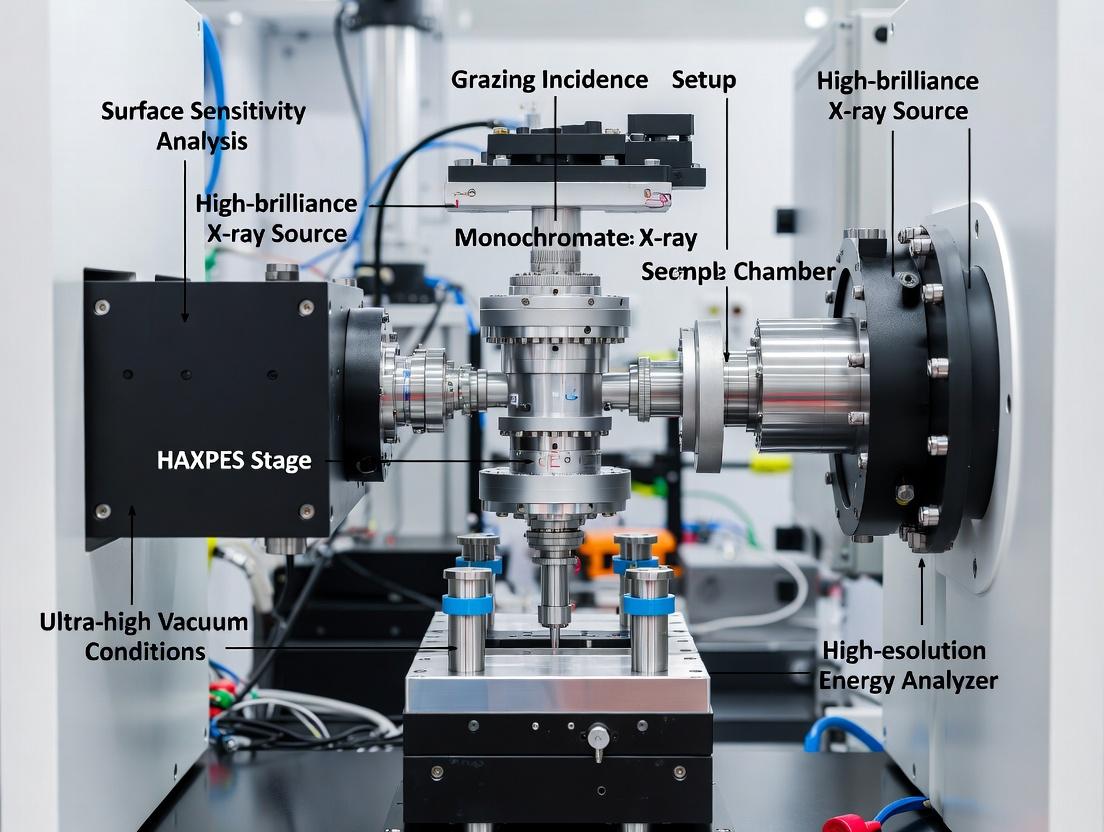
HAXPES at Grazing Incidence: Unlocking Extreme Surface Sensitivity for Drug Development & Biomaterials Research
This comprehensive guide explores the advanced surface analysis technique of HAXPES (Hard X-ray Photoelectron Spectroscopy) at grazing incidence angles.
HAXPES at Grazing Incidence: Unlocking Extreme Surface Sensitivity for Drug Development & Biomaterials Research
Abstract
This comprehensive guide explores the advanced surface analysis technique of HAXPES (Hard X-ray Photoelectron Spectroscopy) at grazing incidence angles. Tailored for researchers, scientists, and drug development professionals, it details how the method dramatically enhances surface and shallow-interface sensitivity for analyzing complex biological and pharmaceutical samples. The article covers foundational principles, practical methodological protocols, strategies for troubleshooting common challenges, and validation against complementary techniques. By bridging fundamental science with applied problem-solving, it serves as an essential resource for leveraging this powerful tool to investigate drug-polymer interactions, thin-film coatings, catalyst surfaces, and biomaterial interfaces with unprecedented chemical-state specificity.
What is Grazing-Incidence HAXPES? Principles of Depth Profiling & Enhanced Surface Sensitivity
This Application Note details the integration of Hard X-ray Photoelectron Spectroscopy (HAXPES) with angle-resolved detection, positioned within the broader thesis of utilizing grazing incidence geometries for enhanced surface and interface sensitivity. The core advantage lies in the combination of increased information depth (2-20 nm) from hard X-rays (2-10 keV) with the depth-profiling capability of angle-resolved measurements, without the need for destructive sputtering. This is critical for analyzing buried interfaces, complex multilayer devices, and operando cells—key challenges in materials science and drug development (e.g., for analyzing solid dosage forms or coated medical implants).
Quantitative Data Comparison
Table 1: Comparative Performance of XPS Modalities
| Parameter | Traditional XPS (Al Kα, 1.486 keV) | HAXPES (Hard X-ray, e.g., Cr Kα, 5.4 keV) | HAXPES with Angle-Resolved Detection |
|---|---|---|---|
| Typical Probe Depth | 3-10 nm | 10-30 nm | Tunable from ~2 nm to full probe depth |
| Information Depth (λ) | ~5-7 nm (for Si 2p) | ~15-20 nm (for Si 1s) | Depth resolution of ~1-2 nm near surface |
| Sampling Depth Control | Limited; requires ion sputtering (destructive) | Bulk-sensitive, but lacks inherent depth resolution | Non-destructive, via take-off angle (θ) variation |
| Key Application | Surface chemistry, ultrathin films (<5nm) | Buried interfaces, bulk electronic structure | Gradient analysis, non-destructive depth profiling |
| Kinetic Energy Example | Si 2p: ~1.4 keV | Si 1s: ~4.8 keV | Core-level intensity vs sin(θ) curves |
Table 2: Comparative Signal & Resolution Data
| Metric | Al Kα Source (1.486 keV) | Cr Kα Source (5.414 keV) | Ga Kα Source (9.251 keV) |
|---|---|---|---|
| Inelastic Mean Free Path (λ) for Si | ~5.2 nm (Si 2p) | ~15.8 nm (Si 1s) | ~25.0 nm (Si 1s) |
| Absolute Energy Resolution (ΔE) | <0.5 eV | ~0.7 - 1.0 eV | ~1.0 - 1.5 eV |
| Relative Depth Sensitivity (λ cos θ) | ~1.3 nm (at 75°) | ~4.1 nm (at 75°) | ~6.5 nm (at 75°) |
Experimental Protocols
Protocol 1: Non-Destructive Depth Profiling of a Buried Organic/Inorganic Interface
Objective: To determine the chemical composition gradient across a polymer coating (~20 nm thick) on a metallic biomedical implant substrate. Materials: HAXPES system with tunable X-ray energy (e.g., Ga Kα, 9.25 keV) and a high-precision, multi-axis goniometer. Procedure:
- Sample Mounting: Secure the sample on a flat, conductive holder. Ensure precise alignment of the surface plane with the goniometer's axis.
- System Calibration: Calibrate the spectrometer's binding energy scale using Au 4f7/2 (84.0 eV) and Cu 2p3/2 (932.7 eV) foils.
- Angular Series Acquisition:
- Set the hard X-ray source to Ga Kα (9.25 keV).
- Acquire survey spectra at a take-off angle (θ) of 90° (normal emission) to identify all elements.
- For key core levels (e.g., C 1s, O 1s, Ti 2p from substrate), perform high-resolution scans at a minimum of 5 take-off angles (e.g., 15°, 30°, 45°, 60°, 75°, 90°). Maintain constant pass energy and step size.
- Ensure the X-ray spot size remains on the same sample region for all angles.
- Data Analysis:
- Plot the normalized intensity (peak area) of a substrate peak (e.g., Ti 2p) and a coating peak (e.g., C 1s) as a function of sin(θ).
- Fit the data using a layered model (e.g., within the SESSA simulation software) to extract layer thickness and composition.
Protocol 2: Operando HAXPES of a Solid Electrolyte Interphase (SEI)
Objective: To monitor the chemical evolution of the buried SEI layer in a solid-state battery during cycling. Materials: Operando HAXPES cell with hard X-ray transparent window (SiNx), potentiostat, hard X-ray source (Cr Kα, 5.4 keV). Procedure:
- Cell Assembly: Assemble the battery cell inside an Ar-filled glovebox, integrating it with the operando HAXPES cell. Ensure electrical contact for cycling.
- Operando Measurement Setup: Mount the cell in the HAXPES chamber. Connect the potentiostat leads. Align the X-ray beam to illuminate the electrode of interest through the window.
- Grazing Incidence Alignment: Set the X-ray beam to a shallow incidence angle (<5° relative to sample surface). This maximizes the path length through the SEI layer, enhancing its signal relative to the bulk electrode.
- Cycling & Spectral Acquisition:
- Begin potentiostatic/galvanostatic cycling protocol.
- At defined states of charge/discharge (e.g., OCV, 0.5V, 0.1V), pause cycling and acquire high-resolution HAXPES spectra of key elements (C 1s, O 1s, F 1s, Li 1s, P 2p).
- Use a take-off angle of 80-90° for maximum bulk sensitivity to probe the buried interface.
- Data Processing: Deconvolute core-level spectra to identify chemical species. Track the intensity ratio of SEI components (e.g., LiF, Li2O) to electrode peaks as a function of cycle number.
Visualizations
HAXPES Depth Profiling Workflow
Core Advantage of HAXPES for Buried Layers
The Scientist's Toolkit: Essential Research Reagent Solutions
Table 3: Key Materials & Reagents for HAXPES Experiments
| Item | Function/Explanation |
|---|---|
| Ga Kα / Cr Kα X-ray Source | High-energy source (9.25 keV / 5.41 keV) to excite deep core levels and increase probe depth. |
| High-Precision Goniometer | Enables accurate angular positioning of sample for take-off angle-dependent measurements. |
| Sputter-Deposited Calibration Foils | Au, Cu, Ag foils for precise binding energy and spectrometer work function calibration. |
| Conductive Adhesive Tape (e.g., Cu Tape) | For mounting insulating samples to prevent charging, compatible with high-energy X-rays. |
| Operando Electrochemical Cell | Specialized sample holder with X-ray transparent window (SiNx) for in-situ/operando studies. |
| Reference Powder Samples | Well-characterized standard powders (e.g., LiFePO4, TiO2) for energy scale validation. |
| Argon Glovebox Integration | For sample preparation and transfer of air-sensitive materials (batteries, organics) without contamination. |
| Depth Profiling Simulation Software | Software like SESSA for modeling angle-resolved data and extracting quantitative depth profiles. |
Grazing Incidence (GI) geometry is a cornerstone technique in surface-sensitive spectroscopy and scattering, most notably applied in techniques like X-ray Photoelectron Spectroscopy (XPS) and its variant, Hard X-ray Photoelectron Spectroscopy (HAXPES). The core principle exploits the phenomenon of total external reflection of X-rays at interfaces. When an X-ray beam impinges on a solid surface at an angle ((\alphai)) smaller than a critical angle ((\alphac)), it does not penetrate deeply into the bulk. Instead, it undergoes total external reflection, creating an evanescent wave that propagates parallel to and decays exponentially within a few nanometers of the surface. This dramatically enhances surface sensitivity by confining the probe (photons) to the surface region, minimizing the signal from the bulk substrate.
Within the thesis context of HAXPES for surface science, GI geometry is pivotal for isolating chemical and electronic states of the topmost atomic layers, interfaces, and thin films, which are critical in fields ranging from catalysis to organic electronics and drug-surface interactions.
Core Principles & Quantitative Data
The critical angle ((\alphac)) is material- and energy-dependent, calculated as: [ \alphac (^{\circ}) \approx \sqrt{\frac{2\delta}{10^{-6}}} ] where (\delta) is the dispersive part of the complex refractive index, (n = 1 - \delta - i\beta). For a given element and X-ray energy, (\delta) is proportional to the electron density.
Table 1: Critical Angles ((\alpha_c)) for Common Materials at Key X-ray Energies
| Material | X-ray Energy (keV) | Density (g/cm³) | (\alpha_c) (degrees) | Evanescent Wave Decay Length (1/e, nm) at (\alphai = 0.5\alphac) |
|---|---|---|---|---|
| Silicon (Si) | 2.0 (Al Kα) | 2.33 | 0.57 | ~3.2 |
| Silicon (Si) | 10.0 (HAXPES) | 2.33 | 0.25 | ~7.1 |
| Gold (Au) | 2.0 | 19.32 | 1.31 | ~1.4 |
| Gold (Au) | 10.0 | 19.32 | 0.57 | ~3.2 |
| Polymeric Film (C-rich) | 2.0 | ~1.2 | 0.40 | ~4.5 |
| Water (H₂O) | 10.0 | 1.00 | 0.23 | ~7.8 |
Table 2: Penetration Depth Comparison: Grazing vs. Normal Incidence
| Incidence Angle ((\alpha_i)) | Effective Probe Depth (Si, 10 keV) | Primary Information Origin |
|---|---|---|
| Normal (90°) | ~10,000 nm (10 µm) | Bulk material |
| 2° | ~100 nm | Intermediate, bulk-dominated |
| 0.5° (~2(\alpha_c)) | ~15 nm | Surface region, thin films |
| 0.12° (~0.5(\alpha_c)) | < 5 nm | Ultra-surface, top atomic layers |
Application Notes for HAXPES Surface Sensitivity
- Ultra-thin Film & Interface Analysis: GI-HAXPES is ideal for probing buried interfaces (e.g., electrode/electrolyte in batteries, gate dielectric/semiconductor) without sputtering damage. The shallow escape depth of high-kinetic-energy photoelectrons combined with GI X-ray confinement provides unmatched interface specificity.
- Contaminant & Adsorbate Mapping: Enables differentiation of surface adsorbates (from ambient or processing) from bulk composition. Essential for studying catalyst surfaces or contamination in pharmaceutical coatings.
- In-situ/Operando Studies: The geometry is compatible with liquid cells and gas-phase reaction chambers, allowing real-time monitoring of surface reactions under relevant conditions for drug dissolution or catalytic processes.
Experimental Protocols
Protocol 4.1: Alignment for Grazing Incidence HAXPES
Objective: Precisely align the X-ray beam to achieve a stable, reproducible grazing incidence angle on the sample surface.
- Sample Mounting: Mount the sample on a multi-axis goniometer (capable of precision in the range of 0.001°). Ensure the sample surface is level (parallel to the translational plane of the stage) using a laser level or internal microscope.
- Beam Finder: Use a downstream beam viewer or diode to locate the direct beam position at a known, large angle (e.g., 2-3°). Record the stage coordinates.
- Finding the Surface (Knife-Edge): a. Move the sample into the beam path, obscuring part of the beam. b. Scan the sample height (Z) or rotation (tilt) while monitoring the beam intensity on the downstream viewer. A sharp intensity drop indicates the beam grazing the sample edge. c. Record the position at the 50% intensity point. Repeat for the opposite edge to define the sample plane.
- Setting the Angle: Calculate the motor movements required to reach the desired (\alpha_i) (e.g., 0.3°) from the found surface position. Execute the movement.
- Fine-Tuning & Validation: Perform a fine angular scan ((\alphai) scan) across the theoretical (\alphac) while monitoring the sample current (drain current) or the intensity of a strong substrate XPS peak. The onset of a sharp increase in signal marks (\alphac). Set the working angle relative to this measured value (e.g., 0.7 x (\alphac)).
Protocol 4.2: Angle-Dependent Depth Profiling
Objective: Non-destructively depth-profile a thin film or surface region by varying the incidence angle.
- Initial Setup: Align the sample per Protocol 4.1. Choose a starting angle well below (\alpha_c) (e.g., 0.2° for Si at 10 keV).
- Spectral Acquisition: a. Acquire wide-scan and high-resolution spectra of core levels of interest (e.g., C 1s, O 1s, Si 1s for an organic film on Si). b. Ensure sufficient signal-to-noise ratio; acquisition time may increase at very shallow angles due to reduced illuminated area.
- Angle Variation: Increase (\alpha_i) in a series of steps (e.g., 0.2°, 0.4°, 0.6°, 0.8°, 1.0°, 1.5°, 2.0°). At each step, repeat spectral acquisition with identical parameters.
- Data Analysis: Plot the normalized intensity ratio of a film-specific peak (C 1s) to a substrate peak (Si 1s) as a function of (\alphai) or (1/\sin(\alphai)). Model the data using an exponential decay or a stratified model to extract film thickness and layer ordering.
Protocol 4.3:In-situLiquid-Phase Surface Reaction Monitoring
Objective: Study the evolution of a solid surface in contact with a liquid (e.g., drug dissolution, corrosion) using a GI-HAXPES compatible liquid cell.
- Cell Preparation: Load the solid sample of interest (e.g., active pharmaceutical ingredient crystal) into the HAXPES liquid cell, which features an X-ray transparent membrane (SiNx or graphene).
- Dry Reference Measurement: Align the sample to GI geometry and acquire reference spectra under ultra-high vacuum (UHV) or inert gas.
- Liquid Injection: Under controlled atmosphere, inject the relevant liquid (e.g., simulated gastric fluid) into the cell chamber, ensuring no bubbles form at the sample surface.
- Real-Time Acquisition: With the beam at a fixed grazing angle (~0.5-0.8 x (\alpha_c) of the solid), initiate time-resolved acquisition of specific core levels.
- Post-Experiment: Drain the cell, perform a final measurement of the wet surface, and optionally dry the sample for post-mortem analysis.
Diagrams
Diagram 1: Grazing Incidence HAXPES Principle (67 chars)
Diagram 2: GI-HAXPES Experimental Workflow (53 chars)
The Scientist's Toolkit: Key Research Reagent Solutions
Table 3: Essential Materials for GI-HAXPES Experiments
| Item | Function in GI-HAXPES | Example/Specification |
|---|---|---|
| High-Precision Goniometer | Provides angular positioning with sub-0.01° accuracy for setting grazing incidence. | 5-axis manipulator with piezo-driven tilt. |
| Monochromatic Hard X-ray Source | Provides high-energy (2-10 keV), focused X-rays for deep core-level excitation and enhanced bulk penetration when needed. | Ga Kα (9.25 keV), monochromated Al Kα (1.49 keV) for softer GI. |
| HAXPES Analyzer | Electron energy analyzer with high transmission for high-kinetic-energy photoelectrons. | Wide acceptance angle (±30°) hemispherical analyzer. |
| UHV-Compatible Liquid Cell | Enables in-situ GI-HAXPES measurements of solid-liquid interfaces. | Features SiNx or graphene windows, fluidic connections. |
| Reference Single Crystals | For alignment calibration and energy scale calibration. | Au(111), Si(100) with native oxide. |
| Sputter Ion Gun | For in-situ surface cleaning prior to GI measurements to remove adventitious carbon. | Ar⁺ or Ar cluster source for gentle cleaning. |
| X-ray Transparent Windows | For in-situ gas or liquid cells. Must withstand pressure differential. | 100 nm thick SiNx membranes. |
| Charge Neutralization System | Essential for insulating samples (e.g., polymers, pharmaceuticals) under GI due to reduced conductivity. | Low-energy electron flood gun combined with Ar⁺ ions. |
In Hard X-ray Photoelectron Spectroscopy (HAXPES), understanding the depth from which information is derived is critical for accurate surface and bulk analysis. Two interrelated but distinct concepts govern this: Probe Depth and Information Depth.
- Probe Depth (XPD): The maximum depth from which photoelectrons can be generated and potentially contribute to the signal. It is primarily determined by the attenuation length of the incoming hard X-ray beam in the material. XPD is typically on the order of micrometers (µm).
- Information Depth (ID) / Escape Depth (λ): The maximum depth from which photoelectrons can escape without losing their characteristic kinetic energy (i.e., without inelastic scattering). It is governed by the inelastic mean free path (IMFP) of the outgoing photoelectron. For HAXPES, with photoelectron kinetic energies of 2-10 keV, the ID ranges from ~5 to 30 nm.
- Escape Depth (λ): Often used synonymously with Information Depth, it is defined as the depth normal to the surface from which a specified percentage (e.g., 95% or 63%) of the detected signal originates.
Quantitative Data Comparison
Table 1: Comparative Depths in HAXPES vs. Conventional XPS
| Parameter | Conventional XPS (Al Kα, 1.5 keV) | HAXPES (Ga Kα, 9.25 keV) | Unit | Notes |
|---|---|---|---|---|
| Typical Photoelectron Kinetic Energy (KE) | 200 - 1400 | 2000 - 8000 | eV | Core-level dependent |
| Inelastic Mean Free Path (IMFP, λ) | 0.5 - 3 | 5 - 30 | nm | "Universal Curve" minimum at ~50-100 eV KE |
| Information Depth (3λ, 95% signal) | 1.5 - 9 | 15 - 90 | nm | Depth for 95% of the detected signal |
| Probe Depth (Incoming X-ray) | ~1 | >10 | µm | 1/e attenuation length of X-rays |
| Primary Application Depth Regime | Surface, Ultra-thin films (<10 nm) | Bulk, Buried Interfaces, Thin Films (10-100 nm) | - |
Table 2: Information Depth for Selected Elements in a Silicon Matrix (HAXPES at 9.25 keV)
| Core Level | Binding Energy (eV) | Approx. KE (eV) | Estimated IMFP λ (nm)* | 3λ Info Depth (nm) |
|---|---|---|---|---|
| Si 1s | 1839 | ~7410 | ~23 | ~69 |
| Au 4f | 84 | ~9165 | ~28 | ~84 |
| SiO₂ O 1s | 532 | ~8715 | ~27 | ~81 |
| Ti 1s | 4964 | ~4285 | ~15 | ~45 |
*Estimates based on TPP-2M formula for Si matrix.
Experimental Protocols for Grazing Incidence HAXPES
Protocol 1: Optimizing Surface Sensitivity via Grazing Incidence Objective: To enhance the surface-specific signal contribution by reducing the effective probe depth of the incoming X-rays. Materials: HAXPES spectrometer with tunable X-ray source (e.g., synchrotron bending magnet/undulator or Ga Kα lab source), multi-axis goniometer sample stage, clean, flat specimen. Procedure: 1. Mounting: Mount the sample on the goniometer. Ensure the surface is aligned to the incident X-ray beam axis (θ = 90° defines normal incidence). 2. Initial Measurement: Acquire a wide-scan spectrum at normal incidence (θ ≈ 90°) to identify elemental peaks. 3. Angle Series: Set the photoelectron take-off angle (TOA) to a fixed, near-normal value (e.g., 80-90°). This defines the detection direction. 4. Incidence Angle Variation: Systematically decrease the X-ray incidence angle (θ) from 90° (normal) to near-grazing angles (e.g., 5-10°). Critical: Ensure the beam footprint does not exceed the sample size. 5. Data Acquisition: At each incidence angle (θ), acquire high-resolution spectra of the core levels of interest (e.g., surface contaminant C 1s, substrate bulk peak). 6. Analysis: Plot the intensity of a surface peak vs. a bulk peak as a function of 1/sin(θ). The slope of this plot provides information about the depth distribution of the respective species.
Protocol 2: Determining Layer Thickness of an Ultra-thin Buried Layer Objective: To measure the thickness of a buried nano-layer (e.g., a metal oxide interlayer in a stack) non-destructively. Materials: Sample with buried planar layer, HAXPES spectrometer with high kinetic energy resolution. Procedure: 1. Reference Measurement: Acquire a spectrum from a pure, bulk reference sample of the buried layer material. 2. Sample Measurement: Acquire high-resolution spectra of the buried layer's core level and the core level of the overlying capping layer material. 3. Peak Deconvolution: Fit the buried layer peak. It will likely consist of two components: one from the bulk of the buried layer and one from the interface with the overlying material (chemically shifted). 4. Intensity Ratio Analysis: Apply a layered model (e.g., using the NIST SESSA software or a simple exponential attenuation model). The intensity ratio (Iburied / Icap) is a function of the overlying layer thickness (d), the IMFP of the photoelectrons in the cap layer (λcap), and the geometric angles. 5. Calculation: Solve for thickness *d* using the formula: Iburied / Icap ∝ [1 - exp(-d / (λcap * sin(TOA)))] / exp(-d / (λ_cap * sin(TOA))).
Diagrams
Diagram 1: Probe Depth vs Information Depth Concept
Diagram 2: Grazing Incidence HAXPES Workflow
The Scientist's Toolkit: Key Research Reagent Solutions
Table 3: Essential Materials for HAXPES Surface Sensitivity Studies
| Item | Function / Role in Experiment | Critical Specifications |
|---|---|---|
| High-Brightness X-ray Source | Generates high-energy photons to probe deep core levels and achieve high bulk sensitivity. | Synchrotron Undulator (tunable) or Ga Kα (9.25 keV), Cr Kα (5.4 keV) lab source. |
| High-Energy, High-Resolution Analyzer | Measures kinetic energy of ejected photoelectrons with minimal aberrations. | Wide acceptance angle, pass energy up to 200-500 eV for survey scans, <1 eV resolution for core levels. |
| Multi-Axis Cryo-Goniometer | Precisely manipulates sample orientation (incidence & take-off angles) and maintains sample integrity. | Angular precision <0.1°, cooling to reduce beam damage, UHV compatibility. |
| Reference Calibration Samples | For energy scale calibration and instrument function verification. | Sputter-cleaned Au foil (Au 4f at 84.0 eV), Cu foil (Cu 2p, Cu 3p), Fermi edge of a metal. |
| Depth Profiling Software | Models photoelectron intensities from layered structures to extract quantitative depth information. | NIST SESSA, QUASES, or custom routines implementing exponential attenuation models. |
| UHV Sample Preparation Chamber | For in-situ cleaning (sputtering, annealing) and thin film deposition to prepare uncontaminated surfaces/interfaces. | Base pressure <5e-10 mbar, integrated sputter gun, electron beam evaporators, sample heating. |
| High-Purity Single Crystals / Substrates | Used as well-defined substrates for thin film growth or as reference bulk samples. | Si(100) with native/thermal oxide, epitaxial grade SrTiO₃, optically flat SiO₂ wafers. |
Hard X-ray Photoelectron Spectroscopy (HAXPES) conducted at grazing incidence angles is a powerful technique for probing the chemical and electronic structure of surfaces, interfaces, and buried layers. A fundamental phenomenon in this geometry is the interaction of the incident X-ray beam with the sample surface near the critical angle for total external reflection. At and below this angle, the X-ray penetration depth is minimized to a few nanometers, drastically enhancing surface sensitivity. Furthermore, under these conditions, an X-ray Standing Wave (XSW) field is generated above the surface due to the coherent interference between the incident and specularly reflected beams. This periodic electric field intensity can be strategically used to amplify the photoelectron signal from specific atomic planes, providing exceptional depth resolution and positional accuracy for adsorbates or dopants. This application note details the protocols and considerations for leveraging these effects in surface science and materials research, with specific relevance to advanced drug delivery system characterization.
Core Principles and Quantitative Data
Critical Angle Parameters
The critical angle ((\thetac)) for total external reflection is material- and energy-dependent, approximated by: [ \thetac (^\circ) \approx \frac{1.65}{E{keV}} \sqrt{\frac{Z\rho}{A}} ] where (E{keV}) is the X-ray energy in keV, (Z) is the atomic number, (\rho) is the density (g/cm³), and (A) is the atomic mass.
Table 1: Critical Angles for Common Materials at Selected HAXPES Energies
| Material | Density (g/cm³) | (\theta_c) at 4 keV (mrad) | (\theta_c) at 8 keV (mrad) | Penetration Depth at (\theta_c) (nm) |
|---|---|---|---|---|
| Si | 2.33 | 4.1 | 2.0 | ~3-5 |
| SiO₂ | 2.65 | 4.4 | 2.2 | ~3-5 |
| Au | 19.3 | 11.2 | 5.6 | ~2-4 |
| Pt | 21.45 | 11.8 | 5.9 | ~2-4 |
| Polymer (C-based) | ~1.0 | ~1.8 | ~0.9 | ~5-10 |
X-ray Standing Wave Characteristics
The XSW period ((D)) is controlled by the incidence angle ((\theta)): [ D = \frac{\lambda}{2\sin\theta} ] where (\lambda) is the X-ray wavelength. By scanning (\theta) through (\theta_c), the antinodes of the standing wave sweep vertically through the sample, modulating the photoelectron yield from atoms at specific heights.
Table 2: XSW Modulation Parameters for a Si Substrate at 4 keV
| Incidence Angle Condition | Standing Wave Period (nm) | Primary Information Gained |
|---|---|---|
| (\theta << \theta_c) | > 100 | Enhanced surface signal, no depth resolution. |
| (\theta \approx \theta_c) | ~2-5 | Maximum surface sensitivity, precise adsorbate height determination. |
| (\theta > \theta_c) | < 2 | Bulk probing, interface analysis. |
Experimental Protocols
Protocol 3.1: Optimizing Grazing Incidence for Surface-Sensitive HAXPES
Objective: To configure a HAXPES experiment for maximum surface signal amplification from a thin organic film on a flat substrate. Materials: High-brilliance synchrotron beamline or lab-based Ga Kα (9.25 keV) source; high-precision 4-6 axis goniometer; high-energy electron analyzer; ultra-high vacuum (UHV) chamber; flat, clean substrate (e.g., Si wafer with native oxide or Au(111)); sample. Procedure:
- Sample Mounting: Mount the sample on the UHV manipulator. Ensure the surface is in the plane defined by the X-ray beam and the analyzer entrance.
- Beam Alignment: Align the incident X-ray beam to the sample surface using a laser or optical telescope. Coarse alignment should be within ±0.5°.
- Angle Calibration: Perform a specular reflectivity scan (monitoring X-ray fluorescence or sample current) around the expected (\thetac). Fit the curve to obtain the precise (\thetac) value for the substrate.
- HAXPES Measurement: a. Set the analyzer to the core-level photoelectron peak of interest (e.g., C 1s, N 1s, or a substrate element). b. Acquire photoelectron spectra at a series of fixed incidence angles: 0.8(\thetac), 0.9(\thetac), (\thetac), 1.1(\thetac), and 1.5(\theta_c). c. For each spectrum, record the integrated peak intensity and background.
- Data Analysis: Plot the normalized peak intensity vs. incidence angle. The maximum surface signal is typically observed at or just below (\theta_c). The intensity modulation with angle contains XSW information.
Protocol 3.2: XSW-HAXPES for Element-Specific Depth Profiling
Objective: To determine the vertical position of specific atoms (e.g., a drug molecule's key element) within a layered structure. Materials: As in Protocol 3.1, with added requirement for high angular resolution (< 0.001°). Procedure:
- Sample Preparation: Prepare a model system with a well-defined layer (e.g., a self-assembled monolayer or a Langmuir-Blodgett film containing Br or S atoms) on a flat, high-Z substrate (e.g., Au).
- High-Resolution Angular Scan: Choose a photoelectron peak from the marker atom (e.g., Br 1s at ~13.5 keV binding energy for 8 keV excitation).
- Perform a fine-angle scan through (\thetac) (e.g., from 0.7(\thetac) to 1.3(\thetac) in 0.01(\thetac) steps). At each angle, acquire a high-resolution spectrum of the chosen peak.
- Simultaneously, acquire the substrate photoelectron peak (e.g., Au 4f).
- Modeling and Fitting: The photoelectron yield (Y(\theta)) is modulated as: [ Y(\theta) = 1 + R(\theta) + 2\sqrt{R(\theta)} \cdot f \cdot \cos[\nu(\theta) - 2\pi Pz / D(\theta)] ] where (R(\theta)) is reflectivity, (\nu(\theta)) is the reflection phase, (f) is the coherent fraction, and (Pz) is the coherent position (atomic height). Fit the experimental (Y(\theta)) for the adsorbate and substrate peaks to extract (P_z).
Visualizations
Title: HAXPES Grazing Incidence Experimental Workflow
Title: X-ray Standing Wave Formation at Grazing Incidence
The Scientist's Toolkit: Research Reagent Solutions
Table 3: Essential Materials and Reagents for Surface-Sensitive HAXPES/XSW Studies
| Item | Function & Relevance | Example/Specifications |
|---|---|---|
| High-Z Single Crystal Substrates | Provide a flat, atomically smooth surface for forming well-defined XSW and model adsorbate systems. | Au(111), Pt(111), or SrTiO₃(001) single crystals. |
| Silicon Wafers (with native oxide) | Standard, readily available flat substrates for polymer/organic film studies. | P-type, ⟨100⟩ orientation, 10 mm x 10 mm chips. |
| Self-Assembled Monolayer (SAM) Precursors | To create well-ordered, uniformly thick organic layers for method calibration. | Alkanethiols (e.g., 1-dodecanethiol) for Au, or silanes (e.g., octadecyltrichlorosilane) for SiO₂. |
| Langmuir-Blodgett (LB) Film Trough & Materials | For depositing highly ordered, multi-layer films of controlled thickness and composition. | Arachidic acid or phospholipids doped with brominated or metallated molecules (marker atoms). |
| Calibrated Reference Samples | For beamline alignment and energy/angle calibration of the HAXPES system. | Sputter-cleaned Au foil (for Fermi edge), patterned Si/SiO₂ depth standards. |
| UHV-Compatible Solvent Cleaners | For in-situ or pre-insertion sample cleaning to remove adventitious carbon. | HPLC-grade acetone, isopropanol; volatile solvents dried and degassed. |
| Doped Polymer or Drug-Loaded Nanoparticle Films | Representative real-world samples for applying the technique. | Poly(lactic-co-glycolic acid) (PLGA) nanoparticles with Br-tagged paclitaxel on Si. |
| Synchrotron Beamtime | Access to high-brilliance, tunable X-ray source for optimal HAXPES and XSW experiments. | Beamlines specialized for in-situ spectroscopy at variable angles (e.g., SPring-8 BL46XU, ESRF ID32). |
Application Note 1: Titanium Implant Surface Oxide Characterization
Context: The bio-integration and long-term stability of titanium-based medical implants are governed by the properties of their native surface oxide layer (TiO₂). Within the thesis framework, HAXPES at grazing incidence is employed to non-destructively probe the chemical states and stoichiometry of this critical oxide-substrate interface, which is buried beneath several nanometers of surface contamination or functional coatings.
Key Quantitative Data: Table 1: HAXPES Analysis of TiO₂ Layers on Medical-Grade Ti-6Al-4V Implants
| Sample Treatment | Oxide Thickness (nm) | Ti⁴⁺/Ti⁰ Ratio | Carbon Contamination (at. %) | O/Ti Stoichiometry |
|---|---|---|---|---|
| As-machined | 3.5 ± 0.5 | 1.2 | 28.5 | 1.8 |
| Acid-etched | 7.2 ± 1.1 | 5.8 | 15.2 | 2.0 |
| Thermal Oxidation | 25.0 ± 3.0 | 99.0 | 8.7 | 2.0 |
| Plasma Sprayed HA Coating | 2.1 (interfacial) | 0.8 | 22.1 | N/A |
Experimental Protocol: HAXPES Analysis of Implant Surfaces
- Sample Preparation: Cut implant material to 10mm x 10mm coupons. Clean ultrasonically in sequential baths of acetone, isopropanol, and ultrapure water (18.2 MΩ·cm) for 10 minutes each. Dry under a stream of Argon.
- HAXPES Setup: Mount sample on a multi-axis goniometer. Use a monochromated Ga Kα X-ray source (photon energy = 9.25 keV). Set beam footprint to 0.5mm x 2.0mm.
- Grazing Incidence Alignment: Set the incident X-ray angle (α) relative to the sample surface to 0.5°, 2.0°, and 5.0° to vary information depth from ~5 nm to ~20 nm.
- Data Acquisition: Acquire wide survey scans (0-6000 eV binding energy) at pass energy of 200 eV. Acquire high-resolution regional spectra for Ti 2p, O 1s, C 1s, Ca 2p, and P 2p at pass energy of 50 eV. Use a flood gun for charge neutralization for insulating samples (e.g., thick oxide, HA coating).
- Data Analysis: Fit Ti 2p spectra with doublet components for metallic Ti⁰ (453.8 eV), Ti²⁺, Ti³⁺, and Ti⁴⁺ (458.5 eV). Calculate oxide thickness using relative intensities of Ti⁰ and Ti⁴⁺ peaks and known inelastic mean free paths.
Diagram 1: HAXPES depth profiling of implant interface.
The Scientist's Toolkit: Implant Surface Analysis Table 2: Essential Reagents & Materials for Implant Surface Studies
| Item | Function |
|---|---|
| Medical-Grade Ti-6Al-4V ELI Alloy | Standard implant substrate material for biocompatibility testing. |
| Ultrapure Water (Type 1) | Prevents inorganic contamination during rinse steps. |
| Argon Sputter Gas (99.9999%) | For surface cleaning and depth profiling in connected UHV systems. |
| Certified XPS Reference Samples (Au, Cu, SiO₂) | For binding energy scale calibration and instrument performance verification. |
| HA (Hydroxyapatite) Nanopowder (99.9%) | Reference material for coating chemistry validation. |
Application Note 2: Organic Thin-Film Drug Delivery Systems
Context: Ultrathin polymeric films (<100 nm) enable controlled drug release. The thesis utilizes HAXPES grazing incidence to quantify the vertical distribution of active pharmaceutical ingredients (APIs) and polymer matrix components without damaging the fragile film, a task challenging for conventional surface techniques.
Key Quantitative Data: Table 3: HAXPES Depth-Resolved Composition of PLGA/Paclitaxel Thin Film
| Take-off Angle (ψ) | Effective Depth (nm) | PLGA C=O (at. %) | Paclitaxel C-O (at. %) | F 1s (API Tracer) (at. %) |
|---|---|---|---|---|
| 10° (Grazing) | 8 | 72.1 | 27.9 | 0.05 |
| 45° (Standard) | 15 | 78.3 | 21.7 | 0.04 |
| 80° (Near-normal) | 25 | 82.5 | 17.5 | 0.02 |
Experimental Protocol: Compositional Depth Profiling of Polymer Films
- Film Fabrication: Prepare a 2% w/v solution of PLGA (50:50) and 0.2% w/v Paclitaxel in anhydrous chloroform. Spin-coat onto clean silicon wafers at 3000 rpm for 60 seconds in a dry N₂ glovebox. Anneal at 60°C for 1 hour under vacuum.
- Non-Destructive HAXPES Profiling: Load sample without any pre-measurement sputtering. Use Al Kα source (1486.6 eV) for higher surface sensitivity complementing bulk-sensitive Ga Kα. Set the analyzer take-off angle (ψ) to 10°, 45°, and 80° relative to the surface plane.
- Core-Level Spectroscopy: Acquire high-resolution spectra for C 1s, O 1s, N 1s, and F 1s (if using fluorinated API). Use a long acquisition time for trace F 1s signal (≥ 30 mins).
- Quantification & Modeling: Deconvolute C 1s peak into components: C-C/C-H (285.0 eV), C-O (286.5 eV), C=O (289.0 eV). Use the intensity ratio of API-specific peaks (e.g., F 1s, N 1s) to polymer matrix peaks (C=O of PLGA) at different ψ to construct a concentration-depth model.
Diagram 2: Non-destructive depth profiling of organic film.
The Scientist's Toolkit: Organic Thin-Film Research Table 4: Essential Reagents & Materials for Organic Film Studies
| Item | Function |
|---|---|
| PLGA (50:50) Resomer | Biodegradable polymer matrix for controlled drug release. |
| Anhydrous Chloroform (99.9+%) | Solvent for spin-coating, prevents polymer hydrolysis. |
| Test Grade Silicon Wafers (P/Boron) | Atomically flat, conductive substrate for film deposition. |
| Fluorinated API Analog (e.g., Flutamide) | Provides a strong F 1s spectroscopic tag for tracking API distribution. |
| Charge Neutralization Flood Gun (Low-energy e-/Ar+ ions) | Essential for analyzing insulating polymer films without charging artifacts. |
Application Note 3: Functionalized Biosensor Interfaces
Context: The performance of label-free biosensors (e.g., SPR, waveguide) depends on the molecular orientation and packing density of self-assembled monolayers (SAMs). Grazing incidence HAXPES provides quantitative elemental and chemical state data from the SAM-active substrate interface, crucial for immobilization chemistry optimization.
Protocol: SAM Quality Assessment on Gold Biosensor Chips
- SAM Formation: Clean gold-coated sensor chips in piranha solution (3:1 H₂SO₄:H₂O₂) CAUTION: Highly exothermic. Rinse thoroughly with water and ethanol. Incubate in 1 mM solution of thiolated probe molecule (e.g., HS-C11-EG6-COOH) in ethanol for 24 hours under inert atmosphere. Rinse with ethanol and dry under N₂.
- Interface-Sensitive HAXPES: Use Cr Kα radiation (5414.7 eV) to enhance bulk sensitivity and probe the S 2p signal from the Au-S bond at the interface. Set grazing incidence angle (α) to 0.8°.
- Critical Spectral Regions: Acquire high-resolution spectra for S 2p (split into S 2p₃/₂ and 2p₁/₂ doublet), Au 4f, C 1s, O 1s, and N 1s. The S 2p region requires high signal-to-noise; use >1 hour acquisition time.
- Data Interpretation: Fit S 2p peaks to identify bound thiolate (S 2p₃/₂ at ~162 eV) versus unbound/disordered sulfur (S 2p₃/₂ at ~163.5 eV). Calculate SAM surface coverage using the attenuated Au 4f substrate signal relative to a bare gold standard.
Diagram 3: Probing SAM interface for biosensors.
How to Implement GI-HAXPES: Protocols for Biomaterials, Pharmaceuticals, and Thin Films
Sample Preparation Strategies for Sensitive Bio-Interfaces and Drug Layers
Hard X-ray Photoelectron Spectroscopy (HAXPES) at grazing incidence is a cornerstone technique in the thesis "Depth-Resolved Electronic Structure Analysis of Functional Interfaces via Grazing-Incidence HAXPES." This approach combines the bulk sensitivity of hard X-rays (2-10 keV) with the surface selectivity afforded by grazing incidence geometry. The shallow escape depth of photoelectrons at grazing emission angles allows for the non-destructive, depth-resolved probing of the outermost 2-10 nm of a sample. This is critical for investigating sensitive, non-uniform layers such as:
- Bio-interfaces: Protein coronas on nanoparticles, immobilized enzyme layers, lipid membranes, and cellular adhesion films.
- Drug Layers: Amorphous solid dispersions, thin-film drug coatings, and surface-enriched polymer-drug matrices.
The paramount challenge is that these layers are easily perturbed by conventional sample handling, vacuum exposure, or X-ray damage. Therefore, robust preparation protocols are essential to preserve their native chemical state and spatial distribution for meaningful HAXPES analysis.
Application Notes & Comparative Data
Table 1: Comparison of Sample Preparation Methods for Sensitive Layers
| Method | Principle | Optimal For | Key Advantages for HAXPES | Critical Limitations |
|---|---|---|---|---|
| Spin-Coating | Radial centrifugal force spreads solution to form a thin film. | Polymer-drug films, homogeneous ligand layers on flat substrates. | Excellent thickness control (10-200 nm). High uniformity. Rapid. | Can induce molecular alignment. Not suitable for viscous bio-fluids or particulate samples. |
| Langmuir-Blodgett (LB) Transfer | Compressing and transferring a monomolecular layer from air-water interface to solid substrate. | Phospholipid bilayers, highly ordered organic monolayers, 2D protein arrays. | Precise monolayer control (∼0.5-3 nm). Unparalleled molecular order. | Technically demanding. Limited to amphiphilic molecules. Can introduce transfer artifacts. |
| Dip-Coating | Controlled withdrawal of substrate from a solution to entrain a liquid film, which dries. | Conformal coatings on complex geometries, hydrogel layers. | Simple. Works on non-planar substrates. Good for stepwise layer-by-layer assembly. | Less thickness uniformity than spin-coating. Thickness depends on withdrawal speed and viscosity. |
| Cryogenic Fixation & Transfer | Rapid freezing (vitrification) of hydrated samples followed by transfer under ultra-high vacuum (UHV) or cryogenic conditions. | Hydrated protein layers, liposomes, biological specimens in native aqueous state. | Preserves native hydrated state. Minimizes vacuum-induced dehydration and radiation damage. | Requires specialized cryo-transfer equipment. Risk of ice crystallization if not frozen rapidly enough. |
| Electrospray Deposition (ESD) | Generating an aerosol of charged microdroplets from a solution that are soft-landed onto a substrate. | Large biomolecules (antibodies), fragile non-covalent complexes, metastable polymorphs. | Gentle, non-thermal deposition. Minimizes conformational denaturation. Can build thick films gradually. | Requires optimization of solvent conductivity and voltage. Lower deposition rate. |
Table 2: Impact of Preparation Artifacts on HAXPES Spectral Features (Quantitative Summary)
| Artifact | Cause | Observed Spectral Shift/Change | Typical Magnitude | Mitigation Strategy |
|---|---|---|---|---|
| Radiation Damage | X-ray-induced bond cleavage or oxidation. | Appearance of new C 1s (C-O, C=O) or N 1s peaks; decrease in original peak intensity. | New peak growth rates of 0.5-2% per minute of beam exposure. | Use cryogenic cooling (≤ -120°C). Reduce flux, use fast detectors. |
| Vacuum Dehydration | Loss of bound water under UHV. | Shift in O 1s peak: decrease in OH/H₂O component (~533.5 eV), increase in oxide/ether component (~531.5 eV). | Can reduce OH/H₂O signal by 30-70% within 30 min. | Cryogenic preparation, in situ humidification cells. |
| Surface Charging | Poor conductivity of organic/drug layers. | Broadening and shifting of all peaks (often >1 eV). | Uncontrolled shifts of 1-5 eV common. | Use ultra-thin substrates (SiNx membranes), low-energy electron flood gun, graphene coating. |
| Molecular Reorientation | Shear forces during spin/dip coating. | Changes in relative intensity of functional group signals with changing emission angle. | Angle-dependent intensity ratios can vary by factor of 2. | Use slower coating speeds, Langmuir-Blodgett for controlled orientation. |
Detailed Experimental Protocols
Protocol 3.1: Cryo-Stabilized Spin-Coating of Amorphous Solid Dispersion (ASD) Films for HAXPES
Aim: Prepare a uniform, 50 nm thick film of a drug-polymer ASD while preventing phase separation and crystallization. Materials: Itraconazole (drug), HPMC-AS (polymer), anhydrous dichloromethane (DCM), 10x10 mm silicon wafer with native oxide, programmable spin coater, argon glovebox, cryo-transfer puck.
- Solution Preparation: In an argon glovebox (<1% RH), dissolve Itraconazole and HPMC-AS at a 50:50 w/w ratio in DCM to a total concentration of 20 mg/ml. Stir magnetically for 4 hours.
- Substrate Pre-treatment: Plasma clean Si wafer for 5 minutes (O₂/Ar plasma) to ensure hydrophilic surface. Transfer to glovebox.
- Spin-Coating: Place substrate on coater in glovebox. Dispense 100 µl solution. Spin at 500 rpm for 5s (spread), then immediately ramp to 3000 rpm for 30s. Film thickness is governed by
t ∝ 1/√(ω)(where ω is angular speed) and solution viscosity. - Immediate Vitrification: Within 15 seconds of coating, plunge the sample into a slushed nitrogen bath (-210°C) held in a dedicated cryo-transfer vessel. This halts molecular mobility.
- Cryogenic Transfer: Under continuous liquid nitrogen cooling, transfer the puck to the pre-cooled (-150°C) manipulator of the HAXPES system using a vacuum suitcase, ensuring no temperature rise above -130°C.
Protocol 3.2: Langmuir-Blodgett Deposition of a Model Lipid Layer
Aim: Transfer a single, tightly packed monolayer of 1,2-dipalmitoyl-sn-glycero-3-phosphocholine (DPPC) onto a solid substrate for interface studies. Materials: DPPC in chloroform (1 mg/ml), ultrapure water (18.2 MΩ·cm), Langmuir-Blodgett trough with dipper, Wilhelmy plate pressure sensor, hydrophilic Si wafer or gold-coated substrate.
- Trough Preparation: Meticulously clean the trough and barriers with chloroform and ethanol. Fill with ultrapure water. Set temperature to 25.0 ± 0.1°C. Set barrier speed to 10 cm²/min.
- Monolayer Formation: Gently apply the DPPC solution dropwise onto the water surface. Allow 15 minutes for chloroform evaporation and monolayer equilibration.
- Compression Isotherm: Slowly compress the barriers while monitoring surface pressure (Π). The target is the solid-condensed phase at Π = 35 mN/m. Pause compression upon reaching target.
- Vertical Transfer: Orient the hydrophilic substrate vertically. Dip the substrate through the monolayer at a constant speed of 2 mm/min during the upstroke. Monitor transfer ratio (∆Asubstrate/∆Abarrier) to confirm ideal 1:1 transfer.
- Post-Transfer: Retract the substrate fully. Carefully raise the barriers to remove the monolayer from the water surface. The substrate now holds a Y-type LB film. Store under nitrogen until HAXPES analysis.
Visualization: Workflows and Pathways
Title: Cryo-HAXPES Sample Prep Workflow for Sensitive Layers
Title: Grazing Incidence HAXPES Surface Sensitivity Principle
The Scientist's Toolkit: Key Research Reagent Solutions
Table 3: Essential Materials for Preparing Bio-Interfaces & Drug Layers
| Item / Reagent Solution | Primary Function | Critical Specification for HAXPES Prep |
|---|---|---|
| Si Wafers with Low-Roughness Oxide | Standard, flat, conductive substrate. | < 0.5 nm RMS roughness. P/Boron doped for conductivity. Pre-cleaned with piranha solution. |
| Silicon Nitride (SiNx) Membrane Windows | Substrate for transmission-mode and charging-free analysis. | 50-200 nm thick membrane. 0.5x0.5 mm window size. Low-stress nitride. |
| Graphene-Coated TEM Grids | Ultrathin, conductive, inert support for nanoparticles or macromolecules. | Single-layer CVD graphene. Holey carbon grid optional for cryo-work. |
| Cryogenic Vitrification System | Preserves hydrated state and prevents radiation damage. | Slushed nitrogen bath (-210°C) or ethane propane mixture. Cryo-transfer shuttle compatible with your spectrometer. |
| Inert Atmosphere Glovebox | For processing air/moisture-sensitive drug compounds. | < 1 ppm O₂ and H₂O. Integrated spin coater or hotplate preferred. |
| Langmuir-Blodgett Trough | For depositing highly ordered mono- and multilayers. | Computer-controlled barriers and dipper. Precise temperature control (±0.1°C). |
| Low-Damage Sputter Coater | For applying ultrathin conductive capping layers. | Able to deposit 1-2 nm of Au, Pt, or Ir. Cool sputter head to minimize thermal load. |
| Hydration Control Cell | For in situ HAXPES analysis under controlled humidity. | Compatible with spectrometer manipulator. Allows relative humidity control from 5% to 95%. |
| Anhydrous, Spectroscopic-Grade Solvents | For dissolving drugs/polymers without introducing contaminants. | DCM, chloroform, DMF. Stored over molecular sieves in glass ampoules. |
Hard X-ray Photoelectron Spectroscopy (HAXPES), operating in the multi-keV range (typically 2-10 keV), enables bulk-sensitive analysis due to increased inelastic mean free paths (IMFPs). However, for surface-sensitive research—crucial for studying catalysts, thin films, corrosion layers, or drug-surface interactions—the geometry of measurement is paramount. By employing grazing incidence angles, the effective probe depth is drastically reduced, confining the excitation volume to the near-surface region. This application note, framed within a broader thesis on HAXPES for surface science, provides a detailed protocol for determining and optimizing the incidence angle to maximize surface sensitivity for researchers and applied scientists.
Core Principle: Incidence Angle and Effective Probe Depth
The effective information depth, d_eff, for a HAXPES experiment at a given photoelectron emission angle, θ, relative to the surface normal is governed by: d_eff = λ * cos(θ) where λ is the inelastic mean free path (IMFP) of the photoelectron. For grazing incidence (angle between incident X-ray beam and sample surface, α_i, approaching 0°), the emission angle θ also becomes shallow if using a forward-scattering geometry. This double-grazing condition minimizes d_eff.
A more precise formulation for the grazing incidence condition considers the X-ray penetration depth. The intensity of X-rays decays exponentially into the material: I(z) = I_0 exp(-z/Λ), where Λ is the X-ray attenuation length. At grazing incidence, Λ is reduced to Λ * sin(α_i), localizing the X-ray excitation near the surface. Thus, surface sensitivity is maximized when both X-ray penetration and photoelectron escape are constrained.
Quantitative Data: IMFP and Attenuation Lengths for HAXPES
The following table summarizes key parameters for common elements and photoelectron lines relevant to HAXPES surface studies. Values are approximated for 6 keV excitation.
Table 1: HAXPES Parameters for Surface Sensitivity Calculation
| Material | Core Level (Approx. KE) | IMFP (λ) at ~6 keV [nm] | X-ray Attenuation Length (Λ) at 6 keV [nm] | Critical Angle for Total External Reflection (α_c) [degrees] |
|---|---|---|---|---|
| Si | Si 1s (~5.5 keV) | ~15 | ~15,000 | ~0.15 |
| Au | Au 4f (~5.8 keV) | ~8 | ~2,000 | ~0.25 |
| SiO₂ | O 1s (~5.3 keV) | ~12 | ~10,000 | ~0.17 |
| TiO₂ | Ti 1s (~5.7 keV) | ~10 | ~7,000 | ~0.20 |
Key Insight: For maximum surface sensitivity, the incidence angle (α_i) should be set at or slightly above the material-specific critical angle (α_c) to utilize the standing wave and enhanced surface field effects, while ensuring sufficient photon flux.
Experimental Protocol: Determining the Optimal Angle
Protocol 1: Incidence Angle Sweep for Surface Signal Maximization
Objective: To find the incidence angle that maximizes the signal from an ultrathin surface layer (e.g., a 2 nm Al₂O₃ film on Si). Materials: See "Scientist's Toolkit" below. Procedure:
- Sample Alignment: Mount the sample on a high-precision goniometer. Using a laser alignment tool or theodolite, ensure the sample surface is coincident with the rotation axis of the goniometer stage.
- Initial Setup: Set the HAXPES analyzer to a take-off angle (emission angle) of 80° from surface normal (10° grazing emission). Select a core level from the surface layer (e.g., Al 1s) and the substrate (e.g., Si 1s).
- Angle Sweep: Starting at an incidence angle (α_i) of 0.5° (above most critical angles), acquire spectra for both core levels. Use a fixed photon flux and acquisition time.
- Iterative Measurement: Decrease α_i in steps of 0.05° down to 0.05°. At each step, record the peak intensity (background-subtracted area) for the surface (Al 1s) and substrate (Si 1s) signals.
- Data Analysis: Calculate the Surface-to-Bulk Ratio (SBR) = (IntensitySurface) / (IntensitySubstrate) for each angle.
- Optimization: Plot SBR vs. α_i. The optimal angle for surface sensitivity is typically where SBR is maximized. This often occurs just above the critical angle of the substrate material.
Protocol 2: Verifying Probe Depth with Angle-Resolved HAXPES (AR-HAXPES)
Objective: To experimentally measure the effective probe depth and confirm surface confinement. Procedure:
- Fixed Grazing Incidence: Set α_i to the optimal value determined in Protocol 1 (e.g., 0.2°).
- Emission Angle Sweep: Vary the analyzer (emission) angle (θ) from near-grazing (e.g., 85°) to more bulk-sensitive (e.g., 45°) in steps.
- Model Fitting: For a known thin film or adsorbate system, fit the intensity decay of the substrate signal as a function of 1/cos(θ). The slope yields λ, and the extrapolated effective probe depth at grazing emission confirms the surface sensitivity achieved.
Visualization of the Optimization Workflow and Physical Principles
Diagram 1: Workflow for Optimizing Incidence Angle
Diagram 2: Incidence Angle Impact on Probe Depth
The Scientist's Toolkit: Essential Research Reagents & Materials
Table 2: Key Materials for Grazing Incidence HAXPES Experiments
| Item | Function & Specification | Importance for Surface Sensitivity |
|---|---|---|
| High-Precision Goniometer | Provides angular control with ≤0.001° resolution. | Essential for precise alignment and reproducible setting of grazing angles. |
| Reference Thin Film Samples | e.g., Thermally grown SiO₂ on Si (2-10 nm), certified thickness. | Used for calibrating the angle-dependent intensity response and verifying probe depth. |
| High-Energy Analyzer | Wide-angle acceptance lens, capable of >5 keV electron detection. | Enables Angle-Resolved (AR) measurements at high kinetic energies. |
| Synchrotron Beamtime | Access to a HAXPES beamline with tunable energy (3-10 keV). | Provides the high-brilliance, monochromatic X-ray source required for grazing incidence experiments. |
| Surface Charge Neutralizer | Low-energy electron flood gun (< 1 eV) combined with adjustable ion source. | Critical for analyzing insulating samples (e.g., polymers, oxides) without distorting spectral lineshape at low angles. |
| In-situ Sputter Gun & Deposition | Ar⁺ ion source and thermal evaporator. | For sample cleaning and deposition of model ultra-thin films to test surface sensitivity protocols. |
Hard X-ray Photoelectron Spectroscopy (HAXPES), operating in the 2-10 keV range, enables bulk-sensitive probing of materials. However, when integrated with grazing incidence (GI) geometries, it becomes a powerful tool for investigating buried interfaces, thin films, and surface-sensitive phenomena with enhanced signal from top layers. This application note, framed within a broader thesis on HAXPES-GI for surface and interface research, provides a detailed comparison of synchrotron and lab-based sources. The selection critically impacts depth resolution, elemental specificity, and experimental feasibility for research in advanced materials and drug development (e.g., studying drug-polymer interfaces in solid dispersions).
Comparative Analysis: Synchrotron vs. Lab-Based HAXPES
Table 1: Core Source Characteristics and Performance Metrics
| Feature | Synchrotron Beamline | Laboratory Source (e.g., Ga Kα, Cr Kα) |
|---|---|---|
| Photon Energy Range | Tunable, typically 2-12+ keV | Fixed (e.g., Cr Kα @ 5414.9 eV, Ga Kα @ 9251.7 eV) |
| Beam Flux | ~10¹² - 10¹³ ph/s/0.1%BW | ~10⁸ - 10⁹ ph/s |
| Spot Size | 10x10 µm² to 500x500 µm² | 100x100 µm² to mm-scale |
| Energy Resolution (ΔE/E) | ~10⁻⁴ (Excellent) | ~10⁻³ (Good) |
| Source Brightness | Extremely High (10¹⁷-10²⁰) | Moderate (10¹⁰-10¹²) |
| Operational Access | Competitive proposal, scheduled beamtime | 24/7 in-house access |
| Cost Model | High capital, low per-experiment | High capital, no per-use fee |
| Key Advantage | Tunability, high flux & resolution | Availability, dedicated set-up |
Table 2: Suitability for HAXPES Grazing Incidence Applications
| Application Goal | Recommended Source | Rationale |
|---|---|---|
| High-Resolution Depth Profiling (GI) | Synchrotron | Tunable energy optimizes probe depth (λ~E^1.7) and surface sensitivity at grazing angles. |
| Chemical State Mapping at Buried Interfaces | Synchrotron | High flux enables high-resolution spectra from ultra-thin interfacial layers in reasonable time. |
| Routine Quality Control of Film Thickness/Composition | Laboratory | High availability ideal for repetitive measurements on similar samples. |
| Time-Resolved / In Operando Studies | Context-Dependent: Fast processes require synchrotron flux; long-term stability tests suit lab sources. | |
| Valence Band Analysis of Bulk Materials | Both | Lab sources sufficient; synchrotron offers superior signal-to-noise for detailed electronic structure. |
Experimental Protocols for HAXPES-GI
Protocol 3.1: Synchrotron Beamline HAXPES-GI Experiment
Aim: To determine the chemical composition and uniformity of a ~5 nm buried interface within a multilayer semiconductor device.
Materials & Sample Prep:
- Sample: Epitaxially grown multilayer device (e.g., III-V heterostructure).
- Mounting: Conductive carbon tape on a standard sample holder. Ensure electrical contact.
- Cleaning: Ex situ ultrasonic cleaning in isopropanol, followed by Ar gas blow-dry. In situ mild Ar⁺ sputtering may be used if beamline end-station permits.
Procedure:
- Beamline Alignment:
- Align beamline optics for desired photon energy (e.g., 4000 eV for optimal Sn 3d cross-section).
- Use beam viewport and downstream diode to maximize flux on sample position.
- Sample Loading & Alignment:
- Load sample into UHV analysis chamber (P < 5x10⁻⁹ mbar).
- Use sample stage motors to position the region of interest at the beam focus and spectrometer focal point.
- Grazing Incidence Alignment:
- Set the incident X-ray angle (θ) to 0.5° - 2° using the goniometer.
- Perform a quick survey scan (wide energy range) of a core-level peak to maximize intensity by fine-tuning θ and sample height (z).
- Data Acquisition:
- Acquire core-level spectra (Sn 3d, In 3d, Ga 2p, As 2p) with pass energy yielding <200 meV resolution.
- Perform angle-resolved series (0.5°, 1°, 2°, 5°) to vary probe depth non-destructively.
- Map a region by raster-scanning the stage, collecting a spectrum per pixel (optional).
- Data Analysis:
- Energy calibrate spectra using adventitious C 1s or known Fermi edge.
- Fit peaks using Shirley/Vegh-Salvi-Chan/Tougaard backgrounds and Voigt functions.
- Calculate depth profiles from angle-resolved data using layer models.
Protocol 3.2: Laboratory HAXPES-GI for Drug Formulation Analysis
Aim: To assess the surface segregation of a polymer excipient in a solid dispersion tablet.
Materials & Sample Prep:
- Sample: Bisected tablet of drug (e.g., Itraconazole) in polymeric matrix (e.g., HPMC).
- Mounting: Use a screw-mounted clamp holder to secure the tablet half, ensuring a flat surface faces analyzer.
- Charge Compensation: Mandatory. Use low-energy electron flood gun and, if available, Ar ion flood gun.
Procedure:
- System Startup:
- Power on lab source (e.g., Ga Kα), high-voltage supply, and spectrometer.
- Allow 1-2 hours for source and electronics stabilization.
- Sample Loading:
- Load sample into fast-entry load-lock chamber.
- Pump down load-lock to <1x10⁻⁶ mbar, then transfer to analysis chamber (P < 5x10⁻⁹ mbar).
- Geometry Optimization:
- Set take-off angle (TOA = 90° - θ) to 10° (grazing emission) for maximum surface sensitivity.
- Manually or via software, translate/rotate sample to align to the spectroscopic field of view.
- Charge Compensation Tuning:
- Acquire a rapid scan of C 1s or a known peak.
- Adjust flood gun current/energy to minimize peak shift and broadening. Use a known internal reference if possible.
- Data Acquisition:
- Acquire high-count, high-resolution spectra of C 1s, O 1s, N 1s, and drug-specific core levels (e.g., F 1s, Cl 2p).
- Acquire survey spectrum for full compositional overview.
- Repeat at TOA = 80° (more bulk-sensitive) to compare.
- Post-Measurement:
- Compare C 1s peak shapes and component ratios between angles. A change in C-O/C-C ratio indicates polymer surface enrichment.
Visualized Workflows and Relationships
HAXPES Source Selection Decision Tree
Synchrotron vs Lab HAXPES-GI Experimental Workflows
The Scientist's Toolkit: Key Research Reagent Solutions
Table 3: Essential Materials for HAXPES-GI Experiments
| Item | Function in HAXPES-GI | Example / Specification |
|---|---|---|
| Conductive Adhesive | Provides electrical and thermal contact between sample and holder, mitigating charging. | Double-sided copper tape, carbon tape, silver paste. |
| UHV-Compatible Sample Holders | Holds sample in precise, reproducible geometry for angle-dependent work. | Plate-style holders with defined troughs for grazing angles. |
| Charge Neutralization System | Essential for insulating samples (polymers, pharmaceuticals, oxides). Floods surface with low-energy charges. | Integrated electron flood gun (0.1 - 10 eV) often combined with Ar ion flood. |
| Sputter Ion Source | For in situ surface cleaning (removing adventitious carbon) or depth profiling. | Ar⁺ gas, 0.5 - 4 keV, rasterable. |
| Reference Materials | For energy scale calibration and system performance checks. | Clean Au foil (Fermi edge, Au 4f), Cu foil (Cu 2p, Cu LMM), Sputtered Al. |
| For Synchrotron Only: | ||
| Beamline-Specific Filters | Absorbs low-energy harmonics from monochromator. | Thin foil of Cu, Al, or Si, depending on fundamental energy. |
| For Drug Development: | ||
| Model Formulation Standards | Controls for method validation. Samples with known drug/excipient distribution. | Physical mixtures vs. solid dispersions with certified composition. |
Data Acquisition Protocols for Buried Interfaces and Multi-Layer Systems
This document details advanced protocols for probing buried interfaces and complex multi-layer systems using Hard X-ray Photoelectron Spectroscopy (HAXPES) at grazing incidence. Within the broader thesis on HAXPES for surface sensitivity, these protocols leverage the tunability of information depth by varying the incident X-ray angle. Grazing incidence conditions enhance surface and interface sensitivity even when using high-energy photons (2-10 keV) that typically probe bulk. This is critical for non-destructive, depth-resolved chemical and electronic state analysis of technologically relevant layered structures, such as battery electrodes, photovoltaic stacks, catalytic coatings, and encapsulated drug delivery systems.
Table 1: Key HAXPES Parameters for Interface Studies
| Parameter | Typical Range for Buried Interfaces | Function & Impact |
|---|---|---|
| X-ray Energy | 2 - 10 keV | Higher energy increases probing depth and reduces surface specificity. Enables access to deeper core levels. |
| Incidence Angle (α) | 0.5° - 5° (grazing) | Critical control parameter. Lower angles increase surface/interface sensitivity by reducing the effective photoelectron escape depth. |
| Information Depth (λ) | ~5 - 30 nm (kinetic energy dependent) | Depth from which ~63% of signal originates. λ ≈ KE^0.7. Grazing incidence reduces effective depth. |
| Depth Resolution | 1 - 5 nm (with angular variation) | Achievable via modeling or angular-dependent measurements. Best at grazing angles. |
| Energy Resolution | < 0.5 eV | Required to resolve chemical shifts in core levels from different layers. |
| Beam Size | 10 - 100 μm | Allows for spatially resolved analysis of interface homogeneity. |
Table 2: Comparison of Data Acquisition Modes
| Mode | Primary Goal | Protocol Synopsis | Key Output |
|---|---|---|---|
| Single-Angle HAXPES | Rapid chemical state survey | Fix α at 1-2° for enhanced interface signal. Acquire wide-scan and high-resolution core-level spectra. | Elemental composition and chemical states averaged over enhanced surface region. |
| Angle-Resolved HAXPES (AR-HAXPES) | Non-destructive depth profiling | Acquire identical core-level spectra at a series of α (e.g., 0.5°, 1°, 2°, 5°, 10°, 15°). Use constant analyzer transmission. | Dataset for modeling concentration/chemical state vs. depth. |
| HAXPES Mapping | Interface homogeneity | Fix α at grazing angle. Raster beam or sample. Acquire core-level intensity or peak position maps. | 2D spatial map of chemical or electronic property variations at the interface. |
Detailed Experimental Protocols
Protocol 1: AR-HAXPES for Buried Interface Chemical State Depth Profiling
Objective: To determine the chemical state distribution as a function of depth across a buried interface (e.g., solid-electrolyte interphase (SEI) on a Li-ion battery anode). Materials: See "Scientist's Toolkit" below. Methodology:
- Sample Mounting & Alignment:
- Mount sample on a high-precision, multi-axis goniometer.
- Using a laser or optical microscope, align the sample surface to coincide with the goniometer's rotation axis (surface height alignment).
- Set the sample normal perpendicular to the analyzer entrance lens (θ = 90° configuration common at synchrotrons).
- Grazing Incidence Alignment (Critical):
- Define α = 0° as the X-ray beam parallel to the sample surface.
- Using a photodiode or the sample current, perform an incident angle scan (e.g., -5° to +5°) to find the angle of total external reflection for the substrate. This defines the true α = 0°.
- Set the starting measurement angle to just above the critical angle (e.g., 0.5°) for maximum surface/interface sensitivity.
- Data Acquisition:
- Select core levels of interest (e.g., O 1s, F 1s, C 1s, Li 1s for SEI).
- For each pre-defined α (e.g., 0.5°, 1°, 2°, 4°, 6°, 10°, 15°), acquire:
- A survey spectrum to monitor overall composition changes.
- High-resolution spectra for all core levels of interest, ensuring sufficient signal-to-noise ratio.
- Constant Analyzer Energy mode and pass energy must be identical for all angles to ensure comparable electron transmission.
- Record all relevant parameters: α, X-ray energy, beam flux, acquisition time.
- Data Processing:
- Apply standard preprocessing: satellite subtraction, Shirley/Tougaard background subtraction, peak fitting with appropriate constraints.
- For each chemical component (peak), plot normalized intensity vs. sin(α). The slope indicates relative depth.
- Employ modeling (e.g., software like
HAXPESfit) to reconstruct a quantitative depth profile of chemical states.
Protocol 2: Buried Interface Stability UnderIn SituStress
Objective: To monitor the chemical evolution of a buried interface (e.g., in an organic photovoltaic stack) under controlled environmental stress. Materials: See "Scientist's Toolkit." Requires an in situ cell compatible with HAXPES. Methodology:
- Baseline Measurement:
- Load the multi-layer sample into the in situ reaction cell.
- Evacuate or fill with inert gas (N₂).
- Perform a detailed Single-Angle HAXPES survey at a fixed grazing incidence (e.g., α = 2°) to establish the baseline state of the buried interface.
- Application of Stress:
- Introduce stressor to the cell. Examples:
- Thermal: Ramp temperature to target (e.g., 80°C) at a controlled rate.
- Chemical: Introduce a reactive gas (O₂, H₂O vapor) at a specific partial pressure.
- Electrical: Apply a bias across the layers (if contacts are present).
- Introduce stressor to the cell. Examples:
- Time-Resolved Monitoring:
- At fixed time intervals (Δt), rapidly acquire high-resolution spectra of key interface-sensitive core levels (e.g., S 2p for P3HT:PCBM interface, N 1s for perovskite interfaces).
- Continue acquisition until spectral changes stabilize or a maximum time is reached.
- Post-Stress Analysis:
- Return to baseline conditions (inert, room temperature).
- Perform a final AR-HAXPES scan series to assess changes in the depth distribution of components compared to the initial state.
- Model data to quantify interface degradation, diffusion, or reaction layer growth.
Visualization of Protocols and Relationships
HAXPES Protocols for Buried Interface Analysis
Grazing Incidence HAXPES Physical Process
The Scientist's Toolkit: Key Research Reagent Solutions & Materials
Table 3: Essential Materials for HAXPES Interface Studies
| Item / Reagent | Function & Application in Protocols |
|---|---|
| High-Precision Goniometer | Enables accurate sample rotation for setting grazing incidence angles (α) to within < 0.05°. Essential for AR-HAXPES. |
| Inert Transfer Chamber (Vacuum Suitcase) | Allows air-sensitive samples (batteries, perovskites) to be prepared in a glovebox and transferred to the HAXPES system without air exposure. |
| In Situ Reaction Cell | A miniature reactor fitting the HAXPES stage, enabling Protocols with controlled gas, temperature, or bias during measurement. |
| Monochromated Hard X-ray Source | Synchrotron beamline or laboratory source (Ga Kα, Cr Kα) providing high flux, tunable energy photons for high-resolution spectra. |
| Reference Sample (Sputtered Au foil) | Used for energy scale calibration (Au 4f₇/₂ at 84.0 eV) and analyzer work function calibration. |
| Conductive Adhesive (Carbon Tape, In-Ga Eutectic) | For mounting insulating or powder samples to prevent charging artifacts during measurement. |
| HAXPES Data Analysis Software (e.g., CasaXPS, HAXPESfit) | For peak fitting, background subtraction, and quantitative depth profile modeling from AR-HAXPES data. |
| Ion Gun (Ar⁺/Gas Cluster) | For optional, gentle surface cleaning prior to measurement or for depth profiling by sputtering between HAXPES scans (destructive). |
This application note details a critical experiment within a broader thesis investigating the use of Hard X-ray Photoelectron Spectroscopy (HAXPES) at grazing incidence for enhanced surface and interface sensitivity. Polymeric drug-eluting stents (DES) present a classic challenge: the surface chemical state of the therapeutic agent directly influences its release kinetics, stability, and therapeutic efficacy. Conventional XPS is limited by its shallow information depth (~5-10 nm), which may not probe the critical drug-polymer interface beneath the topmost layer. This study demonstrates how tunable HAXPES, combined with variable grazing incidence angles, non-destructively profiles the chemical speciation of the drug (e.g., Sirolimus) from the surface into the bulk of the polymer coating (~100 nm depth), correlating findings with in-vitro elution profiles.
Key Research Reagent Solutions & Materials
Table 1: Essential Materials for HAXPES Analysis of Drug-Eluting Stents
| Material/Reagent | Function / Rationale |
|---|---|
| Drug-Eluting Stent Sample | Coated with a thin polymer (e.g., PBMA, PVDF-HFP) containing Sirolimus. Primary test specimen. |
| Reference Sirolimus Powder | High-purity standard for establishing core-level photoelectron fingerprints (C 1s, O 1s, N 1s) of the pristine drug. |
| Uncoated Bare Metal Stent | Substrate control for identifying contributions from the stent alloy (e.g., Co-Cr, Pt-Cr). |
| Polymer-Coated Stent (No Drug) | Control for deconvoluting photoelectron peaks originating from the polymer matrix vs. the drug. |
| HAXPES Synchrotron Beamtime | Access to tunable high-energy X-rays (e.g., 2-10 keV) for deep, element-specific probing. |
| High-Precision Goniometer | Enables precise variation of the incident X-ray angle (θ) relative to the sample surface for depth-profiling. |
| Charge Neutralization System | Essential for analyzing insulating polymer coatings to prevent sample charging artifacts. |
Experimental Protocols
Protocol: Grazing-Incidence HAXPES Depth Profiling
Objective: To non-destructively determine the chemical state distribution of Sirolimus as a function of depth within the polymer coating. Materials: DES sample, reference materials, HAXPES endstation with goniometer. Procedure:
- Mounting: Secure the stent sample flat on the manipulator stage using a conductive, non-contaminating clip. Ensure electrical contact for charge neutralization.
- Alignment: Use the laser/video system to align the sample surface to the rotational axis of the goniometer. Set initial geometry to near-normal emission (e.g., 80° take-off angle).
- Energy Calibration: Acquire a survey spectrum from a clean gold reference at the intended beam energy (e.g., 4 keV). Adjust binding energy scale to set Au 4f7/2 to 84.0 eV.
- Angular Series Acquisition:
- Set the X-ray beam energy to a high value (e.g., 5 keV) to increase probing depth.
- Acquire high-resolution core-level spectra (C 1s, O 1s, N 1s) at a series of grazing incidence angles (θ): 85°, 80°, 75°, 70°, 65° relative to the surface plane.
- Note: Decreasing θ (more grazing) increases surface sensitivity by reducing the effective path length of photoelectrons to the surface.
- Spectral Processing: For each angle, apply charge correction (if needed), subtract a Shirley background, and perform peak fitting using reference spectra from the pure drug and polymer controls.
Protocol: In-vitro Drug Elution Correlation
Objective: To correlate HAXPES-derived chemical state information with drug release kinetics. Materials: DES samples from same batch, phosphate-buffered saline (PBS) with 0.02% Tween 20, HPLC system. Procedure:
- Elution Setup: Immerse individual stents (n=3) in 10 mL of elution medium (PBS + Tween) at 37°C with gentle agitation.
- Sampling: At predetermined time points (1 hr, 6 hr, 24 hr, 72 hr, 168 hr), remove and replace the entire elution medium. Store samples for analysis.
- HPLC Analysis: Quantify Sirolimus concentration in each eluent using a validated reverse-phase HPLC-UV method.
- Post-Elution HAXPES: After 168 hours, retrieve the stents, rinse gently with DI water, dry under nitrogen, and perform HAXPES analysis as per Protocol 3.1 at a single, representative angle.
Data Presentation & Analysis
Table 2: HAXPES-Derived Relative Atomic Concentration (%) of Key Elements vs. Incidence Angle
| Incidence Angle (θ) | Effective Probing Depth (nm)* | C 1s (%) | O 1s (%) | N 1s (%) | F 1s (%) | Sirolimus O/C Ratio |
|---|---|---|---|---|---|---|
| 85° (Most Bulk-Sensitive) | ~100 | 75.2 | 20.1 | 1.1 | 3.6 | 0.267 |
| 80° | ~75 | 74.8 | 20.5 | 1.0 | 3.7 | 0.274 |
| 75° | ~50 | 73.5 | 21.3 | 1.2 | 4.0 | 0.290 |
| 70° | ~30 | 72.1 | 22.0 | 1.3 | 4.6 | 0.305 |
| 65° (Most Surface-Sensitive) | ~15 | 70.5 | 23.5 | 1.5 | 4.5 | 0.333 |
| Pure Sirolimus Ref. | N/A | 70.0 | 24.0 | 1.8 | 0.0 | 0.343 |
| Pure Polymer Ref. | N/A | 78.0 | 16.0 | 0.0 | 6.0 | 0.205 |
*Estimated using the TPP-2M equation for 5 keV photons in a polymer matrix.
Interpretation: The increasing O/C ratio and N concentration at more grazing angles (surface-sensitive) indicate drug enrichment at the coating surface. The decreasing F signal (from the fluorinated polymer) corroborates this. The sub-surface/bulk composition more closely matches the polymer-rich reference.
Table 3: Correlation of Surface Drug State with Cumulative Elution
| Sample Group | HAXPES Surface N/C Ratio | Cumulative Release at 24 hr (%) | Time to 50% Release (hr) |
|---|---|---|---|
| High Surface Drug (Batch A) | 0.021 | 45 ± 5 | 30 |
| Uniform Distribution (Batch B) | 0.015 | 28 ± 3 | 55 |
| Polymer-Rich Surface (Batch C) | 0.008 | 15 ± 2 | >120 |
Visualizations
Diagram 1: GI-HAXPES and Elution Study Workflow (85 chars)
Diagram 2: Grazing Incidence Depth Sensitivity Principle (91 chars)
Diagram 3: Drug State Correlation with Depth & Release (77 chars)
This application note details a protocol for investigating the surface chemical states of transition metal catalyst nanoparticles (NPs) used in enzymatic bioreactors. Within the broader thesis on Hard X-ray Photoelectron Spectroscopy (HAXPES) at grazing incidence, this study demonstrates the technique's unique capability for non-destructive, depth-resolved analysis of buried functional interfaces. Unlike conventional XPS, HAXPES, with its higher excitation energy (e.g., 4-10 keV), increases the inelastic mean free path of photoelectrons, providing greater probe depths (10-30 nm). When combined with grazing incidence angles, this configuration enhances surface sensitivity, allowing us to isolate and quantify the oxidation states at the NP surface (1-5 nm) from the bulk-like core. This is critical for correlating surface chemistry with catalytic activity and stability in liquid-phase bioreactor environments.
Key Research Reagent Solutions & Materials
| Item Name | Function & Rationale |
|---|---|
| Platinum Nanoparticles (3-5 nm) | Model catalyst system for oxidoreductase-driven reactions. High surface area-to-volume ratio maximizes active sites. |
| Silicon Wafer with 100 nm Thermal Oxide | Ultra-flat, conductive substrate for NP deposition, minimizing charging effects during HAXPES analysis. |
| Phosphate Buffered Saline (PBS), pH 7.4 | Simulates physiological bioreactor conditions. Used for controlled electrochemical oxidation of NP surfaces. |
| Calomel Reference Electrode | Provides a stable potential reference during electrochemical treatment of NPs. |
| Anaerobic Glovebox (N₂ atmosphere) | Enables sample transfer and preparation without unintended atmospheric oxidation prior to HAXPES. |
| HAXPES Synchrotron Beamline | Provides high-flux, monochromatic hard X-rays (e.g., 6 keV) with precise incident angle control (5-85°). |
Experimental Protocol: HAXPES at Grazing Incidence
Objective: To determine the depth profile of Pt oxidation states in electrochemically treated Pt NPs.
Procedure:
- Sample Preparation: Dilute colloidal Pt NPs (3-5 nm) in isopropanol. Deposit 50 µL onto a cleaned SiO₂/Si wafer and allow to dry under N₂. Divide the wafer into four segments.
- Electrochemical Treatment: Using a three-electrode cell (Pt NP sample as working electrode, Pt counter, calomel reference), immerse each sample segment in PBS (pH 7.4). Apply a controlled potential for 300 seconds:
- Sample A: +0.2 V (vs. RHE) – Reduced state.
- Sample B: +0.8 V – Mild oxidation.
- Sample C: +1.2 V – Severe oxidation.
- Sample D: Hold at +1.2 V, then cycle to +0.4 V to simulate reactor regeneration.
- Sample Transfer: Rinse treated electrodes with deaerated water, dry under N₂ flow, and immediately transfer to the HAXPES load-lock via an anaerobic transfer vessel.
- HAXPES Data Acquisition:
- Beam Conditions: 6 keV photon energy, beam spot size 50 x 200 µm.
- Angle-Resolved Measurement: For each sample, acquire Pt 4f and O 1s core-level spectra at four grazing incidence angles (α): 15°, 30°, 60°, 80° (relative to surface).
- Detection: Use a high-resolution hemispherical analyzer at normal emission. Pass energy: 50 eV for survey, 20 eV for high-resolution scans.
- Charge Compensation: Use a low-energy electron flood gun if necessary.
- Data Analysis: Fit Pt 4f spectra using Shirley background and Voigt profiles. Constrain doublet separation (∆ = 3.30 eV) and area ratio (4:3 for 4f₇/₂:4f₅/₂). Assign components: Pt⁰ (71.0-71.2 eV), Pt²⁺ (72.2-72.6 eV), Pt⁴⁺ (74.0-74.5 eV). Calculate relative atomic concentrations from integrated peak areas.
Table 1: Relative Concentration (%) of Pt Species at Grazing Incidence (α = 15°)
| Sample | Applied Potential (V) | Pt⁰ (Metallic) | Pt²⁺ (e.g., PtO) | Pt⁴⁺ (e.g., PtO₂) | O/Pt Ratio |
|---|---|---|---|---|---|
| A | +0.2 | 92.5 ± 1.2 | 6.1 ± 0.9 | 1.4 ± 0.5 | 0.15 ± 0.03 |
| B | +0.8 | 68.4 ± 2.1 | 25.3 ± 1.8 | 6.3 ± 1.1 | 0.52 ± 0.06 |
| C | +1.2 | 12.8 ± 1.5 | 41.7 ± 2.3 | 45.5 ± 2.0 | 1.88 ± 0.12 |
| D | +1.2 → +0.4 | 58.9 ± 2.0 | 32.6 ± 1.7 | 8.5 ± 1.2 | 0.71 ± 0.08 |
Table 2: Depth Profiling via Variable Grazing Incidence on Sample C
| Incidence Angle (α) | Effective Probe Depth (nm)* | Pt⁰ (%) | Pt²⁺ (%) | Pt⁴⁺ (%) |
|---|---|---|---|---|
| 15° | ~2.5 | 12.8 | 41.7 | 45.5 |
| 30° | ~5.0 | 18.5 | 43.2 | 38.3 |
| 60° | ~10.0 | 35.6 | 38.9 | 25.5 |
| 80° | ~12.5 | 45.2 | 34.1 | 20.7 |
*Estimated based on electron IMFP and geometry.
Visualized Workflow and Relationships
HAXPES Workflow for Catalyst NPs
NP Depth Probing with Grazing Angle
Challenges & Solutions in GI-HAXPES: Radiation Damage, Charging, and Data Interpretation
1. Introduction: The Challenge in HAXPES Studies Within the context of a broader thesis on Hard X-ray Photoelectron Spectroscopy (HAXPES) at grazing incidence for enhanced surface sensitivity, a fundamental challenge is radiation-induced damage to organic and pharmaceutical samples. High-energy X-ray flux can break bonds, cause mass loss, and induce chemical state changes, compromising data integrity. These protocols outline strategies to monitor, quantify, and mitigate such damage to obtain reliable surface chemical information.
2. Quantifying Radiation Damage: Key Metrics Damage is assessed by tracking changes in spectral features as a function of photon dose (D), calculated as: D = (I × t) / A where I is beam flux (photons/s), t is exposure time (s), and A is beam area (cm²). Critical metrics are summarized below.
Table 1: Quantitative Metrics for Radiation Damage Assessment
| Metric | Definition | Measurement Method | Typical Threshold for Significant Damage |
|---|---|---|---|
| Critical Dose (D₁/₂) | Dose at which signal intensity or specific chemical component is reduced to 50% of its initial value. | Time-series HAXPES, fitting decay curves. | Highly variable: 10⁸ - 10¹¹ photons/cm² for organics. |
| Mass Loss Rate | Rate of decrease in total C 1s or other core-level intensity. | Slope of total normalized intensity vs. dose. | >5% loss per 10⁹ photons/cm². |
| Chemical State Ratio Change | Change in ratio of two characteristic peaks (e.g., C-C/C=O, API/excipient). | Ratio analysis from peak-fitted spectra over time. | >10% deviation from initial ratio. |
| BE Shift Rate | Rate of Binding Energy (BE) shift of a core-level due to charging or degradation. | Linear fit of BE position vs. dose. | >0.1 eV per 10⁹ photons/cm². |
3. Core Mitigation Protocols
Protocol 3.1: Pre-Experiment Viability Assessment
- Objective: Determine sample sensitivity and establish a safe maximum dose.
- Materials: Sample, HAXPES system with fast-entry load-lock, low-current Faraday cup or photodiode for flux measurement.
- Method:
- Mount sample, align for grazing incidence (e.g., 80-85° from surface normal).
- Measure incident flux (I) at the chosen beamline.
- Define a small, sacrificial analysis area.
- Acquire a rapid survey scan (C 1s, O 1s, N 1s, specific element from API).
- Expose area to a pre-defined, low dose (e.g., 1x10⁸ photons/cm²).
- Immediately acquire identical scan.
- Compare peak shapes, FWHM, and BE positions.
- If changes are minimal (<2%), proceed to full dose-response test (Protocol 3.2).
Protocol 3.2: Dose-Response Curve Generation for Damage Threshold Determination
- Objective: Quantify D₁/₂ for key chemical components.
- Method:
- Select a fresh sample area.
- Acquire high-resolution scan of a core-level of interest (e.g., C 1s).
- Expose the same spot to a series of incremental doses (e.g., 1x10⁸, 5x10⁸, 1x10⁹, 5x10⁹ photons/cm²).
- After each dose, acquire an identical high-resolution scan.
- Fit peaks to quantify intensities of specific chemical states (e.g., C-C, C-O, C=O).
- Plot normalized intensity (I/I₀) vs. cumulative photon dose.
- Fit curve to exponential decay model: I/I₀ = A × exp(-D/τ) + C, where τ is the damage constant. D₁/₂ = τ × ln(2).
- Analysis: Set experimental total dose well below the lowest D₁/₂ for components critical to the study.
Protocol 3.3: Active Mitigation via Sample Cooling and Defocused Beam
- Objective: Reduce damage rate during long acquisitions.
- Materials: Cryogenic cooling stage (liquid N₂ or He), motorized beam-defocusing optics.
- Method:
- Cooling: Mount sample on cryo-stage. Cool to -50°C to -150°C prior to and during analysis. Record sample temperature.
- Defocusing: Defocus the incident beam to increase spot area (A) by a factor of 4-10, thereby reducing dose rate (D/t).
- Combined Approach: Use cooling and beam defocusing simultaneously.
- Repeat Protocol 3.2 under these mitigated conditions to quantify improvement in D₁/₂.
Protocol 3.4: Multi-Point Mapping vs. Single-Point Spectroscopy
- Objective: Distribute dose spatially to preserve chemical integrity at each measurement point.
- Method:
- Define a mapping grid (e.g., 5x5 points over 500x500 μm²) on the sample surface.
- Set the beam size to 50-100 μm.
- Program the stage to move to each grid point.
- Acquire a single, short-duration spectrum at each unique point.
- Co-add spectra from all points to create a final "pristine" spectrum where each point received only 1/25th of the total analysis dose.
4. Visualization of Strategies and Workflows
Diagram Title: Radiation Damage Mitigation Decision Pathway
Diagram Title: Dose-Response Experiment Workflow (76 chars)
5. The Scientist's Toolkit: Research Reagent Solutions
Table 2: Essential Materials for Radiation-Sensitive HAXPES Studies
| Item | Function & Rationale |
|---|---|
| Cryogenic Cooling Stage (LN₂/He) | Reduces kinetic energy of radicals and desorption processes, slowing mass loss and bond breaking. Essential for long scans. |
| Conductive Carbon Tape (Low Outgassing) | For mounting powder samples. Provides a conductive path to minimize charging, with minimal volatile components that create background. |
| In-Situ Sputter Deposition Tool | For applying a thin, transparent (to HAXPES), conductive capping layer (e.g., few nm of Au) post-analysis on a sacrificial area to check for charging-induced BE shifts. |
| Fast-Entry Load-Lock Chamber | Minimizes exposure to atmospheric contaminants and allows rapid transfer to the analysis chamber, preserving sample pristine state. |
| High-Sensitivity, Low-Noise Detector (e.g., CMD) | Enables acquisition of usable signal-to-noise spectra with lower photon flux or shorter acquisition times, reducing dose. |
| Beam-Defocusing/Shaping Optics | Allows controlled enlargement of beam footprint, lowering power density (dose rate) on the sample surface. |
| Reference Calibration Sample (Sputtered Au) | Used for precise, regular beam flux measurement via Au 4f photoelectron yield, critical for accurate dose calculation. |
| Atomic Layer Deposition (ALD) System (Ex-situ) | For depositing ultra-thin, conformal inert encapsulation layers (e.g., Al₂O₃) for transport/storage, removable by in-situ gentle Ar⁺ sputtering. |
Hard X-ray Photoelectron Spectroscopy (HAXPES) at grazing incidence is a powerful technique for probing the chemical composition and electronic structure of buried interfaces and thin films with enhanced surface sensitivity. For insulating biomaterials—such as protein films, polymeric coatings, drug-eluting matrices, and tissue-engineered scaffolds—sample charging during analysis poses a significant challenge. It distorts spectral lineshapes, shifts binding energy scales, and can render data uninterpretable. This application note, framed within a broader thesis on optimizing HAXPES for surface-sensitive research on delicate systems, details practical, experimentally validated compensation techniques to mitigate charging, thereby enabling reliable data acquisition from insulating biomaterials.
Core Charging Mechanisms and Quantitative Impact
Sample charging in HAXPES occurs when the flux of emitted photoelectrons is not balanced by an influx of electrons from the sample stage or the environment. For insulating biomaterials, the problem is exacerbated by their low electrical conductivity and susceptibility to beam damage. The table below summarizes the primary effects and their typical magnitude.
Table 1: Quantitative Impact of Uncompensated Charging on HAXPES of Insulating Biomaterials
| Effect | Description | Typical Observed Shift/Deviation | Consequence for Data |
|---|---|---|---|
| Static Charging | Uniform positive surface potential due to electron loss. | +1 eV to >50 eV (shift) | Complete loss of absolute binding energy reference. |
| Differential Charging | Non-uniform potential across heterogeneous sample surface. | Peak broadening (FWHM increase of 0.5 - 5 eV) | Inaccurate chemical state identification, poor quantification. |
| Beam-Induced Instability | Progressive charging or damage altering local conductivity. | Drift of >0.1 eV/min | Non-reproducible spectra, time-dependent artifacts. |
Practical Compensation Techniques: Protocols and Methodologies
The following protocols outline integrated approaches for charge compensation, suitable for commercial HAXPES systems equipped with standard accessories.
Protocol 3.1: Integrated Low-Energy Electron/Flood Gun and Conductive Grid Compensation
This is the most common and effective method for analyzing bulk insulating biomaterials.
Materials & Setup:
- HAXPES system with integrated low-energy flood gun (typically 0.1 – 10 eV electrons).
- High-transmission (80-90%) nickel or gold fine-mesh grid.
- Conductive carbon tape or colloidal graphite paste.
- Sample stage capable of applying a slight bias (optional).
Procedure:
- Sample Mounting: Apply a minimal amount of conductive carbon tape or graphite paste to the back and edges of the insulating biomaterial sample. Avoid contaminating the analysis surface.
- Grid Placement: Carefully place the conductive mesh grid in direct contact with the front surface of the sample. Ensure good electrical contact between the grid and the conductive paste/tape at the sample edges.
- Flood Gun Calibration:
- Insert the sample and establish initial HAXPES analysis conditions (e.g., 3 keV Al Kα, grazing incidence <10°).
- With the flood gun OFF, acquire a wide-scan spectrum. Observe severe charging (shifted, broadened peaks).
- Activate the flood gun at a very low current (e.g., 10 µA) and low bias (0.5-1 eV). Acquire a spectrum of a known adventitious carbon C 1s peak.
- Iteratively adjust the flood gun electron energy and current until the C 1s peak shape stabilizes and reaches its minimum full width at half maximum (FWHM). The optimal setting typically provides just enough low-energy electrons to neutralize the positive surface charge.
- Verification: Acquire a full spectrum. Check for stability over time (sequential acquisitions) and spatial uniformity by mapping a core level peak across the sample.
Diagram: Integrated Charge Compensation Workflow
Title: Charge Compensation Protocol for Bulk Insulating Biomaterials
Protocol 3.2: Ultra-Thin Coating via Sputter Deposition for Film Stability
For biomaterial films prone to degradation, a conformal, ultra-thin conductive coating can be applied.
Materials & Setup:
- Sputter coater equipped with a platinum or gold target.
- Thickness monitor (quartz crystal microbalance).
- Rotating sample stage within the sputter coater.
Procedure:
- Preparation: Place the biomaterial sample in the sputter coater. Use a rotating stage to ensure uniformity.
- Coating Deposition:
- Pump down to high vacuum (≤ 5 x 10⁻⁵ mbar).
- Set a low deposition rate (0.1-0.2 Å/s for Pt/Au).
- Deposit a coating with a target thickness of 1.0 - 1.5 nm. This thickness is critical: it must be less than the inelastic mean free path of the photoelectrons of interest (typically 3-5 nm for HAXPES) to avoid signal attenuation, while providing a conductive percolation network.
- Validation: Transfer the coated sample to the HAXPES system. Acquire spectra with minimal or no flood gun assistance. The coating's core levels (e.g., Pt 4f, Au 4f) can serve as an internal energy reference.
Table 2: Performance Comparison of Key Compensation Techniques
| Technique | Optimal Use Case | Advantages | Limitations | Typical Residual Shift (C 1s) |
|---|---|---|---|---|
| Low-Energy Flood Gun + Grid | Bulk polymers, thick bioceramics, hydrated films. | Non-destructive, tunable, standard equipment. | May not stabilize highly insulating/rough samples. | < 0.2 eV |
| Ultra-Thin Conductive Coating (1-1.5 nm) | Delicate protein layers, organic films, temperature-sensitive samples. | Provides stable reference, reduces beam damage. | Potential chemical interaction, attenuates signal from underlying sample. | < 0.1 eV (referenced to coating) |
| Sample Biasing | Homogeneous, moderately insulating films on a conductive substrate. | Simple, no extra hardware. | Ineffective for thick or freestanding insulators. | Variable (0.1 - 1 eV) |
The Scientist's Toolkit: Research Reagent Solutions
Table 3: Essential Materials for Charge Compensation in Biomaterial HAXPES
| Item | Function | Key Considerations for Biomaterials |
|---|---|---|
| High-Transmission Metal Mesh Grids (Ni, Au, Cu) | Placed on sample surface to distribute flood gun electrons evenly and provide a local conductive pathway. | Gold is inert, preferred for biological samples. Mesh size (e.g., 100 lines/inch) must balance coverage and signal loss. |
| Conductive Carbon Tape & Colloidal Graphite Paste | Creates an electrical path from the sample holder to the sample edges/back and to the conductive grid. | Use sparingly to avoid contamination. Graphite paste can be dissolved post-analysis if necessary. |
| Platinum/Gold Sputter Target (for ~1.5 nm coating) | Source material for depositing an ultra-thin, conformal conductive layer on the sample surface. | Platinum offers finer grain size than gold for thinner continuous films. Critical to calibrate thickness accurately. |
| Low-Energy Flood Gun (Integrated) | Source of low-energy (0.1-10 eV) electrons to neutralize positive surface charge. | Must be finely adjustable in current and energy. Prolonged high current can cause beam damage. |
| Charge Reference Standards (e.g., Sputtered Au, Adventitious Carbon) | Provides a known binding energy for post-acquisition calibration when an internal reference is absent. | Adventitious carbon (C-C/C-H at 284.8 eV) is ubiquitous but can be affected by sample chemistry. |
Data Interpretation and Validation Protocol
Even with compensation, validation is crucial.
Protocol 5.1: Post-Collection Spectral Calibration and Consistency Check
- Internal Reference: If present (e.g., from a controlled contamination or a known component like a poly(ethylene oxide) ether carbon at 286.5 eV), use it to calibrate the spectrum.
- Adventitious Carbon Reference: If no internal standard exists, calibrate the C 1s peak of adventitious hydrocarbon to 284.8 eV. Document this step explicitly, as it is an assumption.
- Peak Shape Analysis: Check the FWHM of core levels from homogeneous regions of the sample. FWHM values should be consistent with conductive analogs of the material and symmetric.
- Survey Scan Consistency: Ensure all expected elements are present and that the wide-scan spectrum does not show abnormal intensity deficits, which could indicate severe differential charging or coating artifacts.
Diagram: Post-Acquisition Data Validation Logic
Title: Validation Logic for Compensated HAXPES Data
Effective charge management is not a one-size-fits-all procedure but a mandatory step for rigorous HAXPES analysis of insulating biomaterials. By integrating the practical mounting and compensation techniques outlined here—specifically the combined flood gun/grid method for bulk samples and the ultra-thin coating for delicate films—researchers can obtain reliable, high-quality data. This enables the full application of grazing incidence HAXPES to advance surface-sensitive research in biomaterial science, drug delivery, and biointerface engineering, providing critical insights into chemical states and elemental distributions without the artifact of charging.
Deconvoluting Overlapping Signals from Surface and Bulk Contributions
Within the broader thesis on Hard X-ray Photoelectron Spectroscopy (HAXPES) at grazing incidence for surface sensitivity research, a central challenge is the quantitative separation of photoelectron signals originating from the surface region from those of the underlying bulk material. HAXPES (using X-rays > 2 keV) inherently probes deeper (tens to hundreds of nanometers) compared to conventional XPS. Employing grazing incidence angles exploits the increased path length of X-rays, enhancing surface sensitivity by reducing the effective probing depth. This application note details protocols and analytical methods for deconvoluting these overlapping contributions, a critical step for accurate surface chemical state analysis in fields ranging from catalysis to organic electronics and drug delivery surface engineering.
Theoretical Background: Signal Depth Dependence
The total measured photoelectron intensity (I_{total}) for a given element and core level is an integration of contributions from different depths. It can be modeled as:
[ I{total}(\theta) = K \int{0}^{\infty} n(z) \exp\left(\frac{-z}{\lambda_e \cos(\theta)}\right) dz ]
where:
- (K) is an instrumental constant.
- (n(z)) is the depth-dependent atomic concentration.
- (\lambda_e) is the effective inelastic mean free path (IMFP) of the photoelectrons.
- (\theta) is the emission angle relative to the surface normal (for grazing emission, (\theta) is large).
- (z) is the depth from the surface.
For a simple two-layer model (surface layer of thickness (d) on a semi-infinite substrate), the signal separates into surface ((Is)) and bulk ((Ib)) components:
[ I{total}(\theta) = Is(\theta) + Ib(\theta) = K ns \lambdae \cos(\theta) \left[1 - \exp\left(\frac{-d}{\lambdae \cos(\theta)}\right)\right] + K nb \lambdae \cos(\theta) \exp\left(\frac{-d}{\lambda_e \cos(\theta)}\right) ]
By measuring the intensity (I{total}) at multiple, carefully chosen grazing incidence angles, one can solve for (ns), (n_b), and (d).
Key Experimental Protocol: Angle-Resolved HAXPES for Depth Profiling
Objective: To experimentally acquire data suitable for deconvoluting surface and bulk signals from a thin film or surface-modified sample.
Materials & Equipment:
- HAXPES spectrometer (e.g., with Ga Kα, Cr Kα, or synchrotron source > 5 keV).
- High-precision, ultra-high vacuum (UHV) compatible goniometer for sample rotation.
- Sample of interest (e.g., a self-assembled monolayer on a metal substrate, a thin oxide layer on a semiconductor).
- Charge neutralizer (if analyzing insulating samples).
- Sputter ion gun (for optional post-measurement cleaning/validation).
Procedure:
- Sample Preparation & Mounting:
- Prepare the sample according to surface science standards (cleaning, deposition in situ or transfer via UHV suitcase).
- Mount the sample on the holder ensuring a flat, uniform surface is presented to the X-ray beam. Ensure good electrical contact.
- Insert into the HAXPES analysis chamber and achieve base pressure (< 5 x 10⁻⁹ mbar).
Spectrometer Alignment & Calibration:
- Align the sample height to the rotation axis of the goniometer using a fiduciary mark or laser pointer.
- Calibrate the 0° position (surface normal aligned to analyzer lens axis) using a known, clean, homogeneous metal standard (e.g., Au foil).
- Set the desired X-ray source and select the analyzer pass energy for optimal intensity/ resolution (e.g., 50-100 eV for survey, 20-50 eV for high-resolution scans).
Data Acquisition at Multiple Angles:
- Begin with a survey spectrum at normal emission (θ = 0°) to identify all elements present.
- Select the core-level peaks of interest for high-resolution scanning (e.g., C 1s, O 1s, a specific metal peak).
- Set the first grazing emission angle (e.g., θ = 70°). Record high-resolution spectra for all peaks of interest, ensuring sufficient signal-to-noise ratio.
- Sequentially rotate the sample to a series of predefined angles (e.g., θ = 0°, 45°, 60°, 70°, 75°, 80°). Maintain the same spot on the sample to ensure consistency.
- At each angle, collect identical high-resolution spectra. Record the precise geometry and measurement time.
- Critical: Monitor the sample for X-ray or beam-induced damage, especially for organics. Adapt exposure times accordingly.
Data Collection Parameters (Example):
- X-ray Source: Ga Kα (9.25 keV)
- Spot Size: 100 x 100 μm²
- Analyzer Pass Energy: 50 eV
- Step Size: 0.05 eV
- Dwell Time: 100 ms/step
- Angles (θ): 0°, 45°, 60°, 70°, 75°, 80°
Data Analysis Protocol: Mathematical Deconvolution
Objective: To fit the angular-dependent intensity data to a model and extract surface and bulk concentrations and layer thickness.
Software Requirements: Data analysis software capable of non-linear curve fitting (e.g., CasaXPS, Origin, IGOR Pro, or custom Python/Matlab scripts).
Procedure:
- Data Pre-processing:
- Import all spectra from different angles.
- Apply consistent energy calibration referencing to a known adventitious C 1s peak (e.g., 284.8 eV) or a substrate Fermi edge.
- Subtract a Shirley or Tougaard background for each core-level peak.
- Integrate the background-subtracted peak area (I_{total}(\theta)) for each peak at each angle.
Model Fitting:
- Construct a table of (I_{total}(\theta)) vs. (\cos(\theta)).
- Assume a model (e.g., a homogeneous overlayer on a homogeneous substrate). Input known or estimated values for (\lambda_e) (calculate using TPP-2M formula).
- Use a non-linear least squares fitting algorithm to fit the data to the two-layer equation (Section 2).
- Fitted Parameters: Overlayer atomic density ((ns)), substrate atomic density ((nb)), and overlayer thickness ((d)).
- Evaluate fit quality using R² and residual plots.
Advanced Fitting (Graded Interfaces):
- For diffuse interfaces, replace the exponential attenuation term with an error function or a multi-slice model.
- Discretize the depth into N layers, each with a variable concentration, and fit the entire dataset globally.
Table 1: Example Angular-Dependent HAXPES Data for a TiO₂ Thin Film on Si
| Emission Angle θ (deg) | cos(θ) | Ti 2p Peak Area (Arb. Units) | O 1s Peak Area (Arb. Units) | Si 1s Peak Area (Arb. Units) |
|---|---|---|---|---|
| 0 (Normal) | 1.00 | 105,400 | 253,100 | 89,500 |
| 45 | 0.71 | 98,200 | 221,500 | 45,300 |
| 60 | 0.50 | 85,600 | 185,400 | 18,900 |
| 70 | 0.34 | 72,100 | 152,200 | 7,050 |
| 75 | 0.26 | 65,300 | 135,500 | 3,850 |
| 80 | 0.17 | 58,400 | 118,800 | 1,210 |
Table 2: Fitted Parameters from Data in Table 1 (Two-Layer Model)
| Parameter | Symbol | Fitted Value | Unit | Physical Interpretation |
|---|---|---|---|---|
| TiO₂ Overlayer Thickness | d | 4.2 ± 0.3 | nm | Thickness of the surface oxide film. |
| Ti Atomic Density | n_s(Ti) | 42 ± 2 | at./nm³ | Density within the TiO₂ layer. |
| O Atomic Density | n_s(O) | 84 ± 4 | at./nm³ | Consistent with ~TiO₂ stoichiometry. |
| Si Substrate Density | n_b(Si) | 50 ± 1 | at./nm³ | Close to pure Si bulk density (~50 at./nm³). |
| Effective IMFP (Ti 2p) | λ_e | 8.5 | nm | Calculated for ~6 keV photoelectrons in TiO₂. |
The Scientist's Toolkit: Research Reagent Solutions
Table 3: Essential Materials for HAXPES Surface-Bulk Deconvolution Experiments
| Item | Function in the Experiment |
|---|---|
| HAXPES Spectrometer | Core instrument providing high-energy X-rays (lab-based Cr Kα, Ga Kα or synchrotron) and a high-transmission electron analyzer to detect high kinetic energy photoelectrons. |
| UHV Goniometer Stage | Allows precise, motorized rotation of the sample to vary the emission angle θ without breaking vacuum, critical for AR-HAXPES. |
| Single-Crystal Substrates (Au(111), SiO₂/Si, HOPG) | Well-defined, atomically flat surfaces used as model substrates for depositing films or adsorbates for fundamental studies. |
| UHV Suitcase/Transfer System | Enables transfer of air-sensitive samples (e.g., organics, battery materials) from gloveboxes or deposition chambers to the HAXPES system without air exposure. |
| In-situ Sputter/Ion Gun | For surface cleaning of standard samples and for performing depth profiling to validate the non-destructive angular method results. |
| Charge Neutralizer (Flood Gun) | Essential for analyzing insulating samples (e.g., polymers, oxides) to compensate for positive surface charge build-up during X-ray irradiation. |
| TPP-2M Calculator Software | Used to calculate the inelastic mean free path (λ) and effective attenuation lengths for photoelectrons in different materials, a key input for models. |
| Advanced Fitting Software (CasaXPS, QUASES) | Software packages with built-in routines for modeling angle-resolved data and depth profiles, facilitating the deconvolution process. |
Visualization Diagrams
Workflow for Angle-Resolved HAXPES Experiment
Signal Deconvolution Principle
Optimizing Signal-to-Noise Ratio for Trace Element Detection at Surfaces
Within the broader thesis on Hard X-ray Photoelectron Spectroscopy (HAXPES) at grazing incidence for extreme surface sensitivity research, optimizing the Signal-to-Noise Ratio (SNR) is paramount. This Application Note details protocols to enhance SNR for detecting trace elements (e.g., dopants, catalytic sites, surface contaminants) at parts-per-million (ppm) levels, crucial for researchers in materials science, semiconductor development, and pharmaceutical surface analysis.
Core Principles of SNR Optimization in HAXPES
SNR in surface-sensitive HAXPES is defined as the ratio of the photoelectron peak intensity (Signal) to the background noise level. For trace detection, maximizing SNR involves enhancing signal generation from the target element and minimizing all noise sources.
Key Factors:
- Signal: Proportional to photon flux, photoionization cross-section, analyzer transmission, and detector efficiency.
- Noise: Originates from instrumental noise (dark current, electronic), inelastic background, and bremsstrahlung radiation.
Table 1: Effect of Experimental Parameters on SNR for Trace Element Detection
| Parameter | Typical Range | Effect on Signal | Effect on Background/Noise | Recommended for Max SNR |
|---|---|---|---|---|
| Incidence Angle | 0.1° - 5° (grazing) | Increases surface signal exponentially | Increases substrate bremsstrahlung | 0.2° - 1° (balance surface sensitivity & flux) |
| Photon Energy (HAXPES) | 2 - 10 keV | Increases probing depth; tunable for resonant cross-sections | Increases bremsstrahlung continuum | Use resonant energy near target element's absorption edge |
| Analyzer Pass Energy | 5 - 200 eV | Higher transmission at higher PE | Degrades energy resolution | Use ≤ 50 eV for high-resolution core levels; higher for survey |
| Slit/Aperture Size | 0.3 - 1.0 mm | Increases accepted signal | Can increase stray electrons | Use largest compatible with required resolution |
| Acquisition Time per Step | 10 - 500 ms | Linear increase in total counts | Increases proportionally with sqrt(time) | Maximize within instrument/beamtime constraints |
| Beam Size (Focused) | 10 - 100 µm | Increases power density on sample | No direct effect on spectral noise | Use smallest spot covering area of interest |
| Sample Temperature | 80 - 300 K | Can reduce thermal broadening | Can reduce thermal diffuse scattering | Cryogenic temperatures recommended if possible |
Table 2: Comparative SNR for Common Trace Elements (Simulated Data for 1 at. ppm, 10 keV, 0.5° incidence)
| Target Element | Core Level | Binding Energy (eV) | Resonant Energy (keV) | Estimated SNR (1 hr scan, high flux) | Critical Parameter for Optimization |
|---|---|---|---|---|---|
| Fe (contaminant) | 1s | 7112 | 7.112 | 8.2 | Use resonant excitation at Fe K-edge |
| La (dopant) | 3d₅/₂ | 836 | 6.0 | 5.7 | Low P.E., high acquisition time |
| F (pharma surface) | 1s | 684 | 0.69 (SOFT) | 2.1* | Use tender X-rays (~1 keV), not HAXPES |
| Pt (catalyst) | 4f₇/₂ | 74 | 2.0 | 12.5 | High cross-section, easy detection |
*Indicates element not optimal for HAXPES detection.
Detailed Experimental Protocols
Protocol 4.1: Sample Preparation for Ultra-Sensitive Surface HAXPES
Objective: Prepare a clean, flat, electrically grounded surface to minimize extrinsic noise.
- Substrate Selection: Use highly-polished, conductive substrates (e.g., Si wafer, Au(111) film).
- Cleaning: Sonicate in sequential solvents (acetone, isopropanol) for 10 minutes each. Dry under Ar/N₂ stream.
- Surface Treatment: Immediately prior to loading, treat with UV-Ozone for 15 minutes or perform Ar⁺ sputter-anneal cycles in UHV (for non-organic samples).
- Application of Analyte: For dopant/contaminant studies, use spin-coating or drop-casting from high-purity solutions. For adsorption studies, use a dedicated UHV deposition system.
- Electrical Grounding: Apply conductive carbon tape or wire to the sample edge to connect to the spectrometer ground, preventing charging.
Protocol 4.2: Instrumental Setup for Grazing Incidence HAXPES SNR Optimization
Objective: Configure the beamline and spectrometer for maximum surface sensitivity and SNR.
- Beamline Alignment:
- Calibrate photon energy using a standard foil (e.g., Cu, Au) absorption edge.
- Optimize beam focus and harmonics rejection using the beamline's monochromator and mirrors.
- Grazing Incidence Alignment (Critical):
- Use a laser level to coarsely align the sample surface parallel to the beam.
- Perform an incidence angle scan (θ) by monitoring the sample drain current or the intensity of a strong substrate peak (e.g., Si 1s) from 0° to 5°.
- Set θ to the angle just before the onset of total external reflection (typically 0.2°-0.5° for 10 keV on Si). This maximizes electric field intensity at the surface.
- Spectrometer Configuration:
- Select a wide acceptance lens mode (e.g., "Large Area" mode).
- Set the entrance slit to the largest width compatible with the desired energy resolution (e.g., 0.8 mm).
- Choose a pass energy of 50 eV for detailed scans and 200 eV for rapid surveys.
- Cool the detector (if applicable) to reduce dark noise.
Protocol 4.3: Data Acquisition Strategy for Trace Element Core Levels
Objective: Acquire spectra with statistically significant counts for the target peak.
- Preliminary Scan: Acquire a wide survey spectrum (e.g., 0-10 keV BE) to identify all elements present and check for charging.
- Region of Interest (ROI) Definition:
- Set the scan window to ±30 eV around the target core level peak.
- Use a step size of 0.1 eV for high-resolution scans.
- Dwell Time Optimization:
- Perform a short test scan (5 min). Estimate the count rate in the peak channel (S) and a background channel (B).
- Calculate required total scan time (T) to achieve a target SNR using: SNR ≈ (S * T) / sqrt((S+2B) * T).
- For ppm-level detection, plan for 8-24 hours of integration per core level, splitting into multiple sweeps to monitor stability.
- Background Characterization: Acquire a spectrum from a clean, otherwise identical reference sample under identical conditions to define the substrate background.
Protocol 4.4: Post-Processing for SNR Enhancement
Objective: Extract the weakest signals from the acquired data.
- Averaging & Alignment: Align all sweep cycles to a reference peak (e.g., adventitious C 1s or substrate peak) and sum them.
- Background Subtraction: Apply a Shirley or Tougaard background model to remove the inelastic secondary electron background.
- Smoothing: Apply a minimal, frequency-based smoothing filter (e.g., Savitzky-Golay) only after background subtraction, ensuring it does not distort peak shape.
- Peak Fitting: Fit the target peak using a Gaussian-Lorentzian lineshape on a linear background. Constrain parameters (FWHM, asymmetry) based on major element peaks in the same spectrum.
Visualizations
HAXPES Grazing Incidence SNR Optimization Workflow
Signal and Noise Pathways in HAXPES
The Scientist's Toolkit: Research Reagent Solutions
Table 3: Essential Materials and Reagents for Surface-Sensitive Trace HAXPES
| Item | Function in Experiment | Key Consideration for SNR |
|---|---|---|
| HAXPES Beamtime | Provides high-energy, tunable, high-flux X-rays. | Synchrotron grade: Select beamline with high brilliance and energy resolution near target element's absorption edge. |
| High-Precision Goniometer | Allows accurate alignment to grazing incidence (<0.1° precision). | Motorized with sub-0.01° steps: Critical for setting optimal incidence angle. |
| UHV-Compatible Cryostat | Cools sample to cryogenic temperatures (≤ 80 K). | Reduces thermal broadening and vibrational noise, enhancing peak sharpness. |
| Charge Neutralization System | Floods sample with low-energy electrons/ions to compensate for photoelectron emission. | Essential for insulating samples to prevent peak shifting and broadening. |
| High-Transmission Electron Energy Analyzer | Collects and energy-filters photoelectrons. | Large acceptance angle and slit maximize signal collection efficiency. |
| Spin Coater | Produces uniform thin films of analyte on substrates for model studies. | Uniformity prevents signal variation and simplifies data interpretation. |
| Ar⁺ Sputter Gun | Cleans sample surfaces in situ within the UHV analysis chamber. | Removes adventitious carbon, revealing the true surface signal. |
| Reference Standard Samples | Calibrate binding energy scale and analyzer transmission function (e.g., Au, Cu, Ag foils). | Traceable standards ensure quantitative accuracy for peak fitting and quantification. |
1. Introduction Within the broader thesis on Hard X-ray Photoelectron Spectroscopy (HAXPES) at grazing incidence for enhanced surface sensitivity, accurate data interpretation is paramount. Angle-dependent measurements are central to this, enabling depth profiling and the isolation of surface signals. However, the derived quantitative information is severely compromised by two pervasive experimental factors: geometric effects (e.g., variable analyzed area and effective path length) and intrinsic sample roughness. This document outlines the theoretical foundations, correction protocols, and data presentation methods essential for reliable analysis.
2. Core Correction Principles
2.1 Geometric Effects As the emission angle (θ, measured from the surface normal) increases, the effective sampling area on the sample surface increases proportionally to 1/cos(θ). Simultaneously, the effective path length of photoelectrons through any overlayer or the sampling depth itself increases by 1/cos(θ). For a perfectly smooth, homogeneous sample, the detected intensity I(θ) for a signal from an infinitely thin layer at depth d is modulated as: I(θ) ∝ exp(-d / (λ cos(θ))) where λ is the inelastic mean free path (IMFP). The raw angular plot is therefore a convolution of this exponential decay with the geometric projection factor.
2.2 Sample Roughness Effects Surface and interfacial roughness scatter photoelectrons, effectively redistributing intensity from specular directions. This attenuates the measured angular anisotropy, mimicking a thicker or more diffuse interface. Commonly used models (e.g., the β-parameter model or the Height-Height Correlation Function model) treat roughness as a damping factor on the ideal angular response.
3. Quantitative Data Summary
Table 1: Impact of Uncorrected Effects on Derived HAXPES Parameters
| Parameter | Effect of Uncorrected Geometry | Effect of Uncorrected Roughness | Typical Magnitude of Error |
|---|---|---|---|
| Layer Thickness | Overestimated at high θ | Significantly overestimated | 20-200% |
| IMFP (λ) | Inaccurate, non-physical values | Overestimated | 30-150% |
| Interface Width | Artificially broadened | Greatly broadened | 50-300% |
| Signal Depth Origin | Skewed towards deeper layers | Indistinct, blurred | Major misassignment |
Table 2: Comparison of Roughness Correction Models
| Model | Key Parameter | Applicability | Complexity |
|---|---|---|---|
| β-parameter (Empirical) | β (0=smooth, 1=fully rough) | Isotropic roughness, quick assessment | Low |
| Height-H Correlation (HHCF) | RMS roughness (σ), correlation length (ξ) | Fractal or correlated roughness | High |
| Effective MLD (EMLD) | Effective multilayer dispersion | Graded interfaces, intermixing | Medium |
4. Experimental Protocols
Protocol 4.1: Angle-Resolved HAXPES Data Acquisition for Correction Objective: Acquire a dataset suitable for subsequent geometric and roughness correction. Materials: HAXPES beamline/source, multi-axis goniometer, sample of interest, reference standard (e.g., Au foil). Procedure:
- Mount the sample ensuring the surface is at the rotational center (phi axis) of the goniometer.
- Using a low-incidence angle (e.g., <5° grazing), align the sample surface by maximizing the specular reflection of a visible laser or optimizing the total electron yield.
- Define θ = 0° as the surface normal. Verify by checking symmetry of a core-level intensity during a small phi rotation.
- Acquire wide-scan spectra at a minimum of 10 emission angles (θ) from 0° (normal) to 80° or the instrument maximum. Ensure constant pass energy and step size.
- Critical Step: At each angle, measure the intensity of a substrate peak with a known, large IMFP (e.g., Si 1s in silicon-based samples) or use a current monitor to record the incident photon flux. This serves as the geometric correction monitor.
- Record all relevant geometric parameters: beam footprint dimensions, analyzer acceptance angle, and angular step accuracy.
Protocol 4.2: Two-Step Data Correction Workflow Objective: Apply sequential corrections to raw angle-dependent intensities. Input: Raw intensity I_raw(θ) for a specific photoelectron peak. Software: Data analysis suite (e.g., Igor Pro, Matlab, Python with SciPy).
Step A: Geometric Correction
- Calculate the geometric projection factor: G(θ) = 1 / cos(θ).
- Account for illuminated area variation: I_geom(θ) = I_raw(θ) / G(θ).
- (Optional/Advanced) Correct for incident beam footprint variation if the sample is smaller than the beam at high θ.
Step B: Roughness Assessment & Correction
- Fit the geometrically corrected data I_geom(θ) for an ideal, smooth layered model (e.g., a single layer on substrate) to extract a first-approximation thickness (d_0) and IMFP (λ_0).
- Compute the residuals. If a systematic damping of the angular modulation is observed, apply a roughness model.
- For β-model: Refit the data using the modified equation: I_fit(θ) = I_0 * exp(-d / (λ cos(θ))) * [1 - β + β * (1/cos(θ))]. The fit parameters are I_0, d, λ, β.
- For HHCF model: Implement a Debye-Waller-like damping factor: I_fit(θ) = I_ideal(θ) * exp[-(4πσ sin(θ) / λ)^2] for uncorrelated roughness, or use the full HHCF formalism for correlated roughness.
- The final corrected parameters describing the material are d and λ from the model fit that includes the roughness term.
5. Mandatory Visualizations
Diagram 1: Core Workflow for Data Correction
Diagram 2: Geometry vs. Roughness Effects
6. The Scientist's Toolkit: Research Reagent Solutions
Table 3: Essential Materials for Angle-Dependent HAXPES Studies
| Item | Function & Rationale |
|---|---|
| High-Precision Multi-Axis Goniometer | Allows accurate angular positioning (θ, φ, χ) with <0.1° reproducibility. Crucial for defining geometry. |
| Optical Surface Alignment Laser | Enables visual pre-alignment of the sample surface to the rotation axis, reducing setup time and error. |
| Atomically Flat Reference Sample (e.g., SiO₂/Si wafer, Au(111)) | Provides a benchmark for assessing instrument alignment and the baseline for "zero roughness" angular response. |
| Roughness Calibration Gratings (with known σ, ξ) | Certified samples with defined RMS roughness (σ) and correlation length (ξ) for validating roughness correction models. |
| Flux Monitor (Mesh or Au Grid) | Placed upstream of the sample to normalize incident photon flux, decoupling intensity variations from beam instability. |
| Kinematic Mount with XYZ & Theta Adjustment | Ensures the sample surface can be precisely positioned at the focal and rotational center of the instrument. |
| Software for NLLS Fitting (e.g., CasaXPS, QUASES, Custom Code) | Implements complex layered models with geometric and roughness correction factors for parameter extraction. |
GI-HAXPES vs. Other Techniques: Validating Findings and Choosing the Right Tool
Within the broader thesis framework utilizing Hard X-ray Photoelectron Spectroscopy (HAXPES) at grazing incidence for enhanced surface sensitivity, the combination of Time-of-Flight Secondary Ion Mass Spectrometry (TOF-SIMS) and Auger Electron Spectroscopy (AES) provides a powerful, complementary analytical triad. HAXPES offers non-destructive chemical state information from buried interfaces (1-10 nm), but for detailed elemental and molecular depth profiling with nanometer-scale resolution, TOF-SIMS and AES are indispensable. This application note details protocols for their integrated use to solve complex materials science problems in thin-film systems, semiconductors, and advanced functional coatings relevant to device development.
The table below summarizes the key parameters and complementary information provided by the three core techniques in this workflow.
Table 1: Complementary Surface and Interface Analysis Techniques
| Parameter | HAXPES (Grazing Incidence) | AES | TOF-SIMS |
|---|---|---|---|
| Primary Information | Chemical state, oxidation state, electronic structure | Elemental composition (Z>2), chemical shifts (minor) | Elemental & molecular species, isotopes, mapping |
| Depth Resolution | 1-10 nm (tunable via angle) | 2-5 nm (for profiling with sputtering) | 1-3 nm (in depth profiling mode) |
| Lateral Resolution | 10s µm to mm (beam size) | ~10 nm (in scanning mode) | 100 nm - 1 µm (imaging mode) |
| Detection Sensitivity | 0.1 - 1 at.% | 0.1 - 1 at.% | ppm - ppb (high mass sensitivity) |
| Destructive? | Non-destructive | Destructive during sputter profiling | Destructive (sputtering) |
| Best For | Non-destructive chemical bonding at buried interfaces | High-res elemental depth profiles & nanoscale mapping | Ultra-trace contamination, organic layers, isotopes |
Experimental Protocols
Protocol 1: Integrated Depth Profile of a Thin-Film Stack (e.g., ALD High-k Dielectric on Si)
This protocol sequences techniques to maximize information from a single sample region.
1. Sample Preparation:
- Material: Silicon wafer with 10 nm Al₂O₃ (ALD) / 2 nm SiO₄Nₓ interlayer.
- Cleaning: Sonicate in isopropanol for 5 minutes, dry with N₂.
- Mounting: Use indium foil or dedicated conductive clips on an ASTM standard holder. Ensure electrical contact for AES/TOF-SIMS.
2. Initial Non-Destructive HAXPES Analysis:
- Tool: Synchrotron-based HAXPES endstation or lab-source with monochromator.
- Parameters: Photon energy: 4-6 keV. Incidence angle: 5° (grazing) for max surface sensitivity.
- Scan: Acquire survey and high-resolution spectra (Si 1s, O 1s, Al 1s, N 1s, C 1s). Use charge neutralizer if needed.
- Outcome: Determine chemical states of Al (Al-O vs. Al-metal), Si (substrate, silicate, nitride), and nitrogen bonding at the buried interface without sputter damage.
3. AES Depth Profiling on Adjacent Area:
- Tool: Scanning Auger Microprobe with Ar⁺ ion sputter gun.
- Parameters: Primary beam: 10 keV, 10 nA. Sputter ion beam: 1 keV Ar⁺, 2x2 mm raster, optimized for uniform crater.
- Profile Setup: Alternate between sputtering (30-60 sec intervals) and AES analysis (peak-to-peak heights for Al KLM, O KLL, Si KLL, N KLL).
- Data Work: Plot atomic concentrations (using relative sensitivity factors) vs. sputter time. Convert time to depth using crater measurement (profilometer).
- Outcome: High-resolution elemental depth profile defining layer thicknesses and interfacial widths with ~3 nm resolution.
4. TOF-SIMS Molecular & Trace Analysis:
- Tool: TOF-SIMS V (or equivalent) with Biₙ⁺ cluster source for analysis, Cs⁺ or O₂⁺ for sputtering.
- Parameters: Analysis: 30 keV Bi₃⁺, static conditions for surface, then dual-beam depth profile. Sputter: 1 keV Cs⁺, 300x300 µm area.
- Profile Setup: Acquire positive/negative ion spectra cyclically. Monitor Al⁺, AlO⁻, Si⁺, SiO⁻, SiO₂⁻, CN⁻, C₂H₄O⁻, etc.
- Data Work: Generate depth profiles for specific molecular fragments and trace contaminants (Na⁺, K⁺, F⁻). Overlay with AES elemental data.
- Outcome: Identify molecular species at interfaces (e.g., hydroxyl groups, organic residues) and trace contaminants at ppb levels not visible by AES/HAXPES.
Table 2: Key Parameters for Integrated Depth Profiling Protocol
| Step | Technique | Primary Beam / Source | Sputter Source | Key Measured Signals | Critical Setting |
|---|---|---|---|---|---|
| 1 | HAXPES | 5 keV X-rays (grazing) | N/A | Al 1s, Si 1s, O 1s, N 1s | Take-off angle = 5° |
| 2 | AES | 10 keV, 10 nA e⁻ beam | 1 keV Ar⁺ | Al KLL, O KLL, Si KLL | Sputter raster > Analysis raster |
| 3 | TOF-SIMS | 30 keV Bi₃⁺ | 1 keV Cs⁺ | Al⁺, Si⁺, SiO⁻, C₂H₄O⁻ | Dual-beam mode, low energy sputter |
Protocol 2: Mapping Surface Contamination & Interface Delamination
For failure analysis of a coated device with suspected interfacial corrosion.
1. Macroscopic HAXPES Survey:
- Perform large-area HAXPES survey (500 µm beam) on delaminated and intact regions. Identify changes in oxidation states (e.g., metal → oxide shift).
2. AES Elemental Mapping:
- Locate the interfacial crack at high magnification (SEM mode).
- Perform AES point analysis inside crack and on adjacent material.
- Create high-resolution (≤50 nm) elemental maps for O, Cl, S, and base metal across the crack interface.
3. TOF-SIMS Molecular Mapping:
- On the same feature, acquire high-lateral-resolution TOF-SIMS images using a Bi₃⁺ or J105⁺ cluster beam.
- Map specific negative ions (Cl⁻, HS⁻, SO₃⁻, organic acids) to identify corrosive agents.
- Perform a shallow depth profile within the mapped area to see if contaminants are surface-only or have penetrated.
The Scientist's Toolkit: Research Reagent Solutions & Essential Materials
Table 3: Essential Materials for TOF-SIMS/AES/HAXPES Experiments
| Item / Reagent | Function / Application |
|---|---|
| Indium Foil | Conductive, malleable mounting substrate for irregular samples; ensures electrical ground. |
| Certified Reference Materials | Thin-film standards (e.g., Ta₂O₅ on Si, Ni/Cr multilayers) for depth profile calibration. |
| Conductive Carbon Tape | Low-outgassing adhesive for mounting insulating powders or fragments. |
| Argon (99.9999%), Cryo Grade | Ultra-high purity sputtering gas for AES and TOF-SIMS to minimize analytical artifacts. |
| Cesium/Iodine Evaporation Sources | For TOF-SIMS, enhances negative/positive ion yields respectively for specific elements. |
| In-situ Cleaving Stage | For creating clean, atomically fresh cross-sections within the UHV chamber for interface analysis. |
| Low-Energy Electron Flood Gun | Essential charge neutralization for insulating samples during AES and TOF-SIMS analysis. |
| ISO 17034 CRM for HAXPES | Calibration standards (Au, Cu, Ag foils) for binding energy scale verification. |
Visualizing the Complementary Workflow
Diagram 1: Logical decision workflow for technique selection.
Diagram 2: Sequential experimental protocol for full interface characterization.
Within the context of advancing surface sensitivity research using Hard X-ray Photoelectron Spectroscopy (HAXPES) at grazing incidence (GI), understanding the comparative information depths of related techniques is paramount. This application note provides a detailed comparison of Grazing Incidence HAXPES (GI-HAXPES), traditional XPS, and Angle-Resolved XPS (ARXPS). It outlines their fundamental principles, quantitative capabilities, and provides specific experimental protocols for their application, particularly in fields like interfacial science and drug development where layered or buried structures are critical.
Fundamental Principles & Information Depth Comparison
The probing depth (δ, where ~95% of the signal originates) is defined as δ = 3λ sin(θ), where λ is the inelastic mean free path (IMFP) of the photoelectrons and θ is the emission angle relative to the surface plane. Key differentiators:
- Traditional XPS: Uses soft X-rays (e.g., Al Kα, 1486.6 eV). Shorter IMFP limits probing to ~5-10 nm at normal emission (θ=90°).
- ARXPS: Uses the same source as traditional XPS but varies θ to manipulate effective depth. Lowering θ decreases effective depth, enhancing surface sensitivity.
- GI-HAXPES: Uses hard X-rays (≥ 2 keV) at a grazing incidence angle (e.g., < 5°). The high energy increases IMFP (allowing bulk probing), while the grazing incidence geometry drastically reduces the effective path length to the analyzer, restoring extreme surface sensitivity.
Table 1: Quantitative Comparison of Technique Parameters
| Parameter | Traditional XPS (Al Kα) | ARXPS (Al Kα) | GI-HAXPES (Cr Kα, 5414 eV) |
|---|---|---|---|
| Typical X-ray Energy | 1.0 - 1.5 keV | 1.0 - 1.5 keV | 2 - 10+ keV |
| Typical IMFP (λ) in SiO₂ | ~3.5 nm | ~3.5 nm | ~10 nm |
| Typical Take-off Angle (θ) | 90° (normal) | 10° - 90° | ≤ 5° (grazing emission) |
| Effective Probing Depth (δ) | ~10 nm (at θ=90°) | ~0.6 - 10 nm (varies with θ) | < 2 nm (at θ=5°) |
| Primary Depth Information | Averaged over top ~10 nm | Depth profiling via angle variation | Extreme surface/Buried interface sensitivity |
| Sample Damage Risk | Medium (soft X-rays) | Medium | Lower (hard X-rays often cause less damage) |
| Information Volume | Surface-near bulk | Depth-resolved surface region | Ultra-surface and buried interfaces |
Experimental Protocols
Protocol 1: GI-HAXPES for a Buried Organic/Inorganic Interface
Objective: To characterize the chemical states at the interface between a polymer film (≈50 nm) and a silicon substrate. Materials: See "Scientist's Toolkit" below. Procedure:
- Sample Preparation: Spin-coat polymer solution onto cleaned Si wafer. Anneal as required. Verify uniform thickness via ellipsometry.
- Instrument Setup:
- Mount sample on a 6-axis manipulator capable of fine angular control (< 0.1° precision).
- Align sample surface to the manipulator's rotation axis (e.g., using a laser level).
- Select hard X-ray source (e.g., Cr Kα, 5414 eV or Ga Kα, 9251 eV).
- Set analyzer pass energy to 50-100 eV for survey, 20-50 eV for high-resolution scans.
- Grazing Incidence Alignment:
- Set the sample so the surface plane is nearly parallel to the analyzer input lens (θ ≈ 0°).
- Perform a fine θ-scan (e.g., 0° to 5°) while monitoring a substrate core-level intensity (e.g., Si 1s). The intensity will maximize at the optimal grazing angle.
- Data Acquisition:
- Acquire survey spectrum at optimized grazing angle.
- Acquire high-resolution spectra of key peaks: C 1s, O 1s, Si 1s, Si 2s.
- Charge Compensation: Use low-energy flood gun (< 5 eV) if needed. Hard X-rays often induce less charging.
- Data Analysis:
- Fit C 1s peak to identify polymer components and potential interface reactions.
- The Si 1s/2s signal originates from electrons traveling through the polymer overlayer, providing chemical state information of the buried interface.
Protocol 2: ARXPS Depth Profiling of a Surface-Modified Layer
Objective: To determine the thickness and composition gradient of a self-assembled monolayer (SAM) on a gold substrate. Materials: SAM-coated Au substrate, XPS system with angle-resolved capability. Procedure:
- Sample Preparation: Immerse Au substrate in SAM solution, rinse, and dry. Transfer to XPS without contamination.
- Instrument Setup:
- Use Al Kα source.
- Ensure analyzer acceptance cone is small relative to angular changes.
- Data Acquisition:
- Acquire high-resolution spectra (C 1s, S 2p, Au 4f) at a minimum of 5 take-off angles (e.g., 15°, 30°, 45°, 60°, 75°).
- Keep all other parameters (X-ray spot, pass energy) constant.
- Data Analysis (Layer Thickness):
- Use the ratio of substrate (Au 4f) intensities at two angles or a full exponential attenuation model.
- Thickness d can be calculated via: I(θ) = I₀ exp[-d/(λ sin θ)], where I(θ) is the attenuated substrate intensity.
Protocol 3: Traditional XPS for Surface Composition
Objective: Rapid survey of elemental surface composition and contamination. Procedure:
- Mount sample at standard position (typically θ = 45° or 90°).
- Acquire a wide survey scan (e.g., 0-1200 eV binding energy).
- Acquire high-resolution scans of all identified elemental peaks.
- Use relative sensitivity factors (RSFs) to calculate atomic concentrations.
Visualization of Technique Concepts and Workflow
Diagram Title: Technique Selection Decision Workflow
Diagram Title: Schematic Comparison of XPS Techniques
The Scientist's Toolkit: Key Research Reagent Solutions
Table 2: Essential Materials for Surface Analysis Experiments
| Item | Function/Benefit | Example Use Case |
|---|---|---|
| Single-Crystal Substrates (Si, SiO₂, Au(111)) | Provide atomically flat, well-defined surfaces for model studies. | SAM formation, thin-film growth calibration. |
| Certified Reference Materials (Cr, Au, Cu foils) | Essential for binding energy scale calibration and spectrometer function checks. | Daily instrument calibration pre-measurement. |
| Charge Compensation Flood Gun (Low-energy e⁻/Ar⁺) | Neutralizes surface charging on insulating samples, enabling accurate analysis. | Analysis of polymers, oxides, or biological films. |
| In-situ Sample Cleaver/Fracture Stage | Creates clean, uncontaminated interfaces inside the UHV chamber. | Studying buried interfaces in layered devices. |
| Sputter Ion Source (Gas Cluster Ion Beam preferred) | For gentle depth profiling of organic materials and cleaning surfaces. | Removing adventitious carbon or shallow profiling. |
| High-Precision 6-Axis Manipulator | Enables accurate alignment for grazing incidence geometry (<0.1° precision). | Critical for GI-HAXPES experiments. |
| Model Polymer Solutions (PS, PMMA, PVP) | Well-characterized systems for validating depth profiling protocols. | Testing ARXPS or GI-HAXPES analysis methods. |
Synergy with Grazing-Incidence X-ray Diffraction (GIXD) and X-ray Reflectivity (XRR)
Within the broader thesis on Hard X-ray Photoelectron Spectroscopy (HAXPES) at grazing incidence for enhanced surface sensitivity, the synergistic combination of Grazing-Incidence X-ray Diffraction (GIXD) and X-ray Reflectivity (XRR) emerges as a powerful correlative methodology. While HAXPES provides elemental and chemical state information from buried interfaces and thin films, GIXD and XRR deliver complementary nanoscale structural data. This application note details protocols for integrated GIXD-XRR analysis, targeting researchers in surface science and drug development who require comprehensive characterization of organic thin films, self-assembled monolayers, and pharmaceutical formulations.
Table 1: Comparative Outputs of GIXD and XRR Techniques
| Parameter | Grazing-Incidence X-ray Diffraction (GIXD) | X-ray Reflectivity (XRR) | Synergistic Information Gain |
|---|---|---|---|
| Primary Information | In-plane crystalline structure, lattice parameters, crystallite size & orientation. | Film thickness, density, and interfacial roughness (layer-by-layer). | Complete 3D structural map (in-plane order + vertical architecture). |
| Probed Depth | Controlled by α_i (typically 0.1° - 0.5°), can be surface-specific (~5-20 nm) or penetrate deeper. | Entire film stack; extremely surface sensitive to electron density profile normal to surface. | Correlates surface/near-surface crystallinity with overall film morphology. |
| Key Output Metrics | Lattice spacing (d-spacing), crystallite coherence length, texture, unit cell. | Thickness (Å), density (g/cm³), roughness (Å) for each layer. | Links crystalline quality to layer integrity and interface sharpness. |
| Typical Resolution | In-plane Qxy: ~0.001 Å⁻¹. Out-of-plane Qz: ~0.01 Å⁻¹. | Thickness: ±1-2 Å. Density: ±0.01-0.02 g/cm³. Roughness: ±1-2 Å. | Enables modeling where density informs electron density for diffraction, roughness explains peak broadening. |
| Sample Requirements | Requires some degree of in-plane long-range order. | Requires smooth, layered structures; works on amorphous and crystalline materials. | A single sample can be fully characterized if it has both layered structure and in-plane order. |
Table 2: Representative Data from Integrated GIXD-XRR Study on a Pharmaceutical Thin Film
| Analysis Method | Measured Property | Value | Interpretation |
|---|---|---|---|
| XRR | Total Film Thickness | 352 ± 2 Å | Confirms target deposition thickness. |
| XRR | Layer Density | 1.18 ± 0.02 g/cm³ | Suggests porous crystalline form or low packing density. |
| XRR | Substrate-Film Roughness | 8 ± 1 Å | Indicates relatively sharp, conformal interface. |
| GIXD (Primary Peak) | In-plane d-spacing | 18.5 Å | Corresponds to molecular side-chain stacking distance. |
| GIXD | Crystallite Coherence Length | 250 Å | Domains are smaller than the film thickness, suggesting polycrystallinity. |
| Synergy | Structural Model | Tilted crystalline domains within a 352 Å layer. | GIXD explains lower density; XRR confines domains vertically. |
Experimental Protocols
Protocol 1: Sample Preparation for Correlative GIXD-XRR-HAXPES
Objective: Prepare a smooth, homogeneous thin film on a polished, low-roughness substrate (e.g., silicon wafer, quartz) suitable for all three techniques.
- Substrate Cleaning: Sonicate substrate in successive baths of Hellmanex III (2%), deionized water, and ethanol (HPLC grade) for 15 minutes each. Dry under a stream of nitrogen or argon.
- Thin Film Deposition (Spin-coating):
- Prepare a solution of the active material (e.g., organic semiconductor, drug compound) in an appropriate solvent (e.g., toluene, chloroform) at a concentration of 5-10 mg/mL.
- Filter the solution through a 0.2 μm PTFE syringe filter.
- Dispense 100-200 μL onto the static substrate. Spin at 500 rpm for 5 s (spread cycle), then immediately accelerate to 2000-4000 rpm for 30-60 s (thin film cycle).
- Anneal on a hotplate at a temperature below substrate deformation or compound degradation (e.g., 80-150°C) for 10-30 minutes in a nitrogen glovebox.
Protocol 2: Sequential XRR and GIXD Measurement on a Synchrotron Beamline
Objective: Collect high-resolution XRR and GIXD data from the same sample spot to ensure direct correlation.
- Beamline Setup & Alignment:
- Use a high-brilliance, monochromatic X-ray source (e.g., synchrotron beamline with Si(111) double-crystal monochromator, λ = 0.5-1.5 Å).
- Mount the sample on a high-precision 6-circle diffractometer or a dedicated goniometer with horizontal geometry.
- Align the sample surface to the incident beam axis (ω = 0) using a laser and downstream ionization chamber. Fine-tune using a direct beam scan.
- XRR Data Collection:
- Set the detector (typically a point or 1D detector) at 2θ = 0°. Use slits to reduce background.
- Perform a θ/2θ scan. Typical range: 0° ≤ 2θ ≤ 5-10° (Q_z up to ~0.5-1.0 Å⁻¹). Step size: 0.002-0.01°.
- Normalize reflected intensity (I) to the incident beam intensity (I₀) measured via a beam monitor or direct beam scan.
- GIXD Data Collection (Immediately After XRR, Same Spot):
- Fix the incident angle (αi) just below the critical angle of the film (~0.1-0.2°) for supreme surface sensitivity, or slightly above (~0.3°) to probe the entire film.
- Use a 2D pixelated detector (e.g., Pilatus, Eiger) placed perpendicular to the incident beam.
- Perform a rocking scan (phi rotation) or a stationary exposure to capture in-plane Bragg peaks (Qxy). Integration time depends on flux and sample scattering power.
- Data Reduction:
- XRR: Plot log(I/I₀) vs. Qz. Fit data using a Parratt formalism or similar recursive algorithm (e.g., in Motofit, GenX).
- GIXD: Integrate the 2D diffraction image azimuthally to generate 1D intensity vs. Qxy plots. Calibrate Q-space using a known standard (e.g., silver behenate).
Protocol 3: Data Integration and Model Refinement
Objective: Create a unified structural model consistent with both XRR and GIXD datasets.
- Primary XRR Modeling:
- Construct a layered model (substrate / interface / film / air).
- Refine parameters (thickness, density, roughness) for each layer until the simulated curve matches the experimental XRR data.
- Incorporating GIXD Constraints:
- Use the film thickness and density from XRR as fixed parameters in GIXD analysis.
- The crystallite size from GIXD peak broadening should be consistent with (or less than) the layer thickness from XRR.
- If GIXD shows texture, use this to inform the electron density profile model in XRR (e.g., anisotropic density).
- Unified Refinement: Use software capable of simultaneous fitting (e.g., BornAgain, Dioptas with custom scripts) to minimize the residual between the experimental data and a model that simulates both the reflectivity and diffraction patterns.
Visualizations
Title: Synergistic HAXPES-GIXD-XRR Analysis Workflow
Title: GIXD vs XRR Measurement Geometry
The Scientist's Toolkit
Table 3: Essential Research Reagent Solutions & Materials
| Item | Function/Description | Critical Specification |
|---|---|---|
| High-Purity Solvents (Toluene, Chloroform, etc.) | For dissolving thin film materials without impurities that disrupt crystallization. | Anhydrous, ≥99.9%, stored over molecular sieves. |
| Polished Single-Crystal Substrates (e.g., Silicon wafers) | Provide an atomically smooth, flat, and well-defined surface for film growth and analysis. | Prime grade, with native oxide (SiO₂), RMS roughness < 5 Å. |
| Hellmanex III or Micro-90 | Aqueous cleaning concentrate for removing organic and particulate contamination from substrates. | 1-2% dilution in ultrapure water (18.2 MΩ·cm). |
| PTFE Syringe Filters (0.2 μm pore size) | Remove undissolved aggregates or dust from coating solutions to prevent film defects. | Hydrophobic for organic solvents. |
| Calibration Standards (e.g., Silver Behenate, LaB₆) | For accurate calibration of the scattering vector (Q) in GIXD measurements. | NIST-traceable or well-characterized d-spacing. |
| XRR Modeling Software (Motofit, GenX, Parratt32) | To fit XRR data and extract thickness, density, and roughness parameters. | Implements Parratt recursive formalism. |
| GIXD Analysis Suite (GIDVis, DAWN, Fit2D) | For integrating 2D diffraction images and analyzing in-plane peak positions & widths. | Capable of azimuthal integration and Q-space conversion. |
1. Introduction & Thesis Context Within the broader thesis on Grazing-Incidence Hard X-ray Photoelectron Spectroscopy (GI-HAXPES) for surface sensitivity research, a critical challenge is linking the rich chemical-state and compositional data from surfaces/interfaces to functional biological outcomes. This document provides a protocol for correlating GI-HAXPES analysis of bio-functionalized surfaces with downstream cellular assays, enabling researchers to move beyond surface characterization to predictive biological understanding.
2. Experimental Workflow: From Surface to Assay
Diagram Title: Workflow for Correlating Surface Chemistry and Biofunction
3. Detailed Protocols
Protocol 3.1: Substrate Preparation & Bio-Functionalization
- Objective: Create a reproducible, ultra-clean, and well-defined surface for biomolecule immobilization.
- Materials: (See Section 5: Scientist's Toolkit).
- Method:
- Sonicate silicon wafers with Au/Ti adhesion layer in acetone, then isopropanol (5 min each). Dry under N2 stream.
- Clean in UV-ozone cleaner for 20 minutes.
- Incubate in 1 mM thiolated peptide/protein solution in degassed PBS (pH 7.4) for 18 hours at 4°C in a humidity chamber.
- Rinse thoroughly with sterile PBS and Milli-Q water to remove physisorbed molecules. Dry under gentle N2.
Protocol 3.2: In-situ GI-HAXPES Measurement
- Objective: Obtain quantitative elemental and chemical state information from the bio-organic layer (1-10 nm) with minimal radiation damage.
- Instrument Setup: Synchrotron-based HAXPES endstation. X-ray energy: ≈ 4-6 keV. Grazing incidence angle (α): 0.5° - 2.0° (tunable for depth profiling). Chamber pressure: < 1e-9 mbar. Sample cooling: -10°C to reduce beam damage.
- Measurement:
- Transfer functionalized substrate under inert atmosphere to HAXPES load-lock.
- Align sample to achieve desired grazing incidence angle using laser/CCD alignment.
- Acquire survey spectrum (0-6000 eV binding energy) to identify all elements present.
- Acquire high-resolution spectra for core levels: C 1s, N 1s, O 1s, S 2p, Au 4f. Pass energy: 50-100 eV, step size: 0.05-0.1 eV.
- Critical: Acquire a "damage check" scan by repeating a core level at the start and end of the sequence; >5% intensity change invalidates data.
- Use a low flux density (< 1e12 photons/s/µm²) and defocused beam.
Protocol 3.3: Parallel Functional Cell Adhesion Assay
- Objective: Quantify cellular response to the characterized surfaces.
- Method:
- Prepare identical functionalized substrates in triplicate in a sterile 24-well plate format.
- Seed relevant cells (e.g., HUVECs for adhesion studies) at 2.5 x 10^4 cells/cm² in serum-free medium.
- Incubate at 37°C, 5% CO2 for 4 hours.
- Gently wash with PBS 3x to remove non-adherent cells.
- Lyse adherent cells with 0.1% Triton X-100. Measure lactate dehydrogenase (LDH) activity or DNA content using fluorescence (e.g., CyQUANT) to quantify cell number.
4. Data Correlation & Presentation
Table 1: Correlative Data Table from Model Peptide (RGD) Functionalization Study
| Sample ID | GI-HAXPES Metric (S 2p @ ~162 eV) | Surface N/C Atomic Ratio | Biological Assay Result (HUVEC Adhesion) |
|---|---|---|---|
| Au Control | Thiolate Peak Area: 0 ± 50 a.u. | 0.00 ± 0.01 | Cell Count: 1,250 ± 210 (Baseline) |
| Low RGD Density | Thiolate Peak Area: 2,850 ± 300 a.u. | 0.05 ± 0.01 | Cell Count: 8,750 ± 950 |
| High RGD Density | Thiolate Peak Area: 11,200 ± 500 a.u. | 0.12 ± 0.02 | Cell Count: 24,300 ± 1,800 |
| Scrambled Peptide | Thiolate Peak Area: 10,500 ± 600 a.u. | 0.11 ± 0.02 | Cell Count: 2,100 ± 400 |
Data are presented as mean ± SD (n=3 for HAXPES, n=6 for biological). a.u. = arbitrary units.
Table 2: Key HAXPES Spectral Fitting Parameters for Bio-Organic Layers
| Core Level | Binding Energy Range (eV) | Typical Component (Assignment) | FWHM Constraint (eV) |
|---|---|---|---|
| C 1s | 284.0 - 289.0 | C-C/C-H (284.8 eV) | 0.9 - 1.2 |
| C-N/C-O (286.2 eV) | |||
| O=C-O/N-C=O (288.0-288.5 eV) | |||
| N 1s | 398.0 - 402.0 | -NH2 / -NH- (399.5-400.0 eV) | 1.0 - 1.3 |
| -N+/- (401.0-401.5 eV) | |||
| S 2p | 161.0 - 164.0 | S 2p3/2 (Thiolate, Au-S, 162.0 eV) | 0.7 - 1.0 (2p3/2-2p1/2 doublet) |
| S 2p3/2 (Unbound/Disulfide, 163-164 eV) |
Correlation Pathway Logic:
Diagram Title: Data Correlation Informs Rational Surface Design
5. The Scientist's Toolkit: Research Reagent Solutions
| Item / Reagent | Function & Rationale |
|---|---|
| Au-coated Si Wafers (Ti adhesion layer) | Provides an atomically flat, chemically inert, and HAXPES-compatible conductive substrate for thiol-based chemistry. |
| Thiolated Biomolecules | Enable covalent, oriented immobilization on Au surfaces via stable Au-S bonds, crucial for reproducible layers. |
| HAXPES-Compatible Sample Holder | Conductive, non-magnetic holder (e.g., Cu or Mo) with flat, kinematic mounting for precise angle alignment. |
| Inert Atmosphere Transfer Kit | Enables movement of air-sensitive bio-samples from solution to UHV without contamination or oxidation. |
| Synchrotron Beamtime | Essential for accessing high-flux, tunable hard X-rays (>4 keV) required for probing buried interfaces with high SNR. |
| Serum-Free Cell Culture Medium | Used in functional assays to eliminate confounding adhesion factors from serum, isolating surface-bioactivity. |
| Quantitative Cell Assay Kit (e.g., CyQUANT) | Provides a sensitive, fluorescent DNA-based method to count adhered cells on opaque test substrates. |
| XPS Data Processing Software (e.g., CasaXPS) | Industry-standard for rigorous peak fitting, quantification, and depth profiling of HAXPES spectra. |
Grazing-Incidence Hard X-ray Photoelectron Spectroscopy (GI-HAXPES) provides unparalleled, non-destructive chemical state information from buried interfaces and thin films (1-10 nm depth). Within the broader thesis on utilizing GI-HAXPES for surface-sensitive research, validating its findings is paramount to eliminate artifacts and confirm interpretations. This document outlines a rigorous validation framework employing independent, complementary techniques.
Complementary Validation Methodologies & Data Correlation
GI-HAXPES results, such as chemical shift identification, layer thickness, and depth-dependent composition, must be confirmed through orthogonal methods.
Table 1: Core GI-HAXPES Outputs and Corresponding Validation Techniques
| GI-HAXPES Output | Primary Validation Technique | Secondary Validation Technique | Key Correlated Parameter |
|---|---|---|---|
| Elemental Composition & Stoichiometry | Rutherford Backscattering Spectrometry (RBS) | Elastic Backscattering Spectrometry (EBS) | Atomic concentration (%) |
| Layer Thickness & Density | X-ray Reflectivity (XRR) | Ellipsometry | Thickness (Å), Density (g/cm³) |
| Chemical State & Bonding | Soft X-ray PES (SX-PES) | Fourier-Transform Infrared Spectroscopy (FTIR) | Binding Energy (eV), Functional Groups |
| Crystalline Structure & Phase | Grazing-Incidence X-ray Diffraction (GIXRD) | Raman Spectroscopy | Lattice Parameters, Phase ID |
| Morphology & Roughness | Atomic Force Microscopy (AFM) | Scanning Electron Microscopy (SEM) | RMS Roughness (nm), Grain Size |
Table 2: Quantitative Data Correlation Example: SrTiO₃ Thin Film Analysis
| Technique | Measured Parameter | Result | Uncertainty |
|---|---|---|---|
| GI-HAXPES (Ti 2p) | Ti⁴⁺/(Ti³⁺+Ti⁴⁺) Ratio | 0.87 | ±0.03 |
| SX-PES (Ti 2p) | Ti⁴⁺/(Ti³⁺+Ti⁺) Ratio | 0.85 | ±0.05 |
| GI-HAXPES | Sr:Ti Atomic Ratio | 0.95:1 | ±0.05 |
| RBS | Sr:Ti Atomic Ratio | 0.98:1 | ±0.03 |
| GI-HAXPES (ML) | Top Layer Thickness | 32 Å | ±5 Å |
| XRR | Layer 1 Thickness | 34 Å | ±2 Å |
Detailed Experimental Protocols
Protocol 1: Validation of Chemical States using Soft X-ray PES
- Objective: To corroborate chemical bonding states identified by GI-HAXPES with higher surface-sensitive SX-PES.
- Sample Prep: Use identical sample cleave or deposition batch. Conduct SX-PES after GI-HAXPES to avoid soft X-ray surface modification.
- Instrumentation: Synchrotron beamline with tunable soft X-ray source (200-2000 eV).
- Procedure:
- Transfer sample under inert atmosphere to avoid air exposure.
- Acquire survey spectrum to confirm elemental presence.
- Acquire high-resolution spectra for core levels of interest (e.g., C 1s, O 1s, N 1s) at two emission angles (90° and 15°) to assess surface sensitivity.
- Use photon energy to set a similar escape depth (λ) to the GI-HAXPES measurement for direct comparison.
- Apply identical data processing: Shirley background subtraction, calibration using adventitious C 1s (284.8 eV), and consistent peak fitting constraints (FWHM, spin-orbit splitting).
- Validation Criteria: Binding energy shifts and component ratios between species must agree within experimental uncertainty (±0.1-0.2 eV).
Protocol 2: Validation of Thickness/Composition using X-ray Reflectivity & RBS
- Part A – XRR:
- Use a high-resolution X-ray diffractometer with Cu Kα source.
- Align sample for grazing incidence (ω ~ 0°).
- Scan 2θ from 0.1° to 5-10° with fine step size (0.005°).
- Fit the critical angle and Kiessig fringes using a layered model (e.g., in GenX or Motofit) to extract layer thickness, density, and interfacial roughness.
- Part B – RBS:
- Use a He⁺ ion beam with energy 1-2 MeV.
- Align sample normal 10-20° off the beam direction to enhance depth resolution.
- Use a detector at 160° backscattering angle.
- Simulate the RBS spectrum using software (e.g., SIMNRA) with the layer structure and composition from GI-HAXPES/XRR as the input model.
- Validation Criteria: The layered model must simultaneously fit the XRR fringe pattern and the RBS elemental yield edges within chi-squared (χ²) tolerance.
Visualizations
Validation Workflow for GI-HAXPES Results
Iterative Validation Protocol Logic
The Scientist's Toolkit: Research Reagent Solutions
Table 3: Essential Materials for GI-HAXPES Validation Studies
| Item | Function & Application |
|---|---|
| Single-Crystal Reference Substrates (e.g., SiO₂/Si, SrTiO₃) | Provides atomically flat, well-characterized surface for initial method calibration and as a calibration standard for binding energy. |
| Certified Thin Film Reference Materials (e.g., NIST Standard) | Enables cross-technique validation (XRR, RBS, HAXPES) on a sample with known thickness and composition. |
| Inert Atmosphere Transfer Vessel (e.g., Vacuum Suitcase) | Maintains sample integrity (prevents oxidation/contamination) between GI-HAXPES and SX-PES or other UHV techniques. |
| Conducting Adhesive Tape (Carbon, Copper) | For mounting insulating samples to mitigate charging during SX-PES and SEM analysis, ensuring accurate BE measurement. |
| Sputter-deposited Metal Films (Au, Pt, Cr) | Used as calibration overlayers for in-situ thickness validation and for creating well-defined test structures for RBS/XRR. |
| Ion Source (Ar⁺, C₆₀⁺) with Sputter Rate Calibrants (Ta₂O₅, SiO₂) | For controlled depth profiling. Calibrated source is essential for correlating sputter time with depth across techniques. |
| Synchrotron Beamtime Access | Critical for performing SX-PES and high-resolution GIXRD validation with tunable energy and high flux. |
Conclusion
HAXPES at grazing incidence represents a paradigm shift in surface-sensitive analysis, offering researchers in drug development and biomaterials a uniquely powerful tool to probe the crucial chemical makeup of topmost layers and shallow buried interfaces with hard X-ray penetration and robustness. By mastering its foundational principles (Intent 1), implementing robust methodologies (Intent 2), overcoming practical experimental hurdles (Intent 3), and validating data within a broader analytical context (Intent 4), scientists can extract unprecedented insights into surface functionalization, drug-polymer interactions, and corrosion or passivation layers. Future directions point toward in-situ and operando GI-HAXPES studies of biological interfaces in liquid cells, high-throughput screening of combinatorial material libraries, and tighter integration with computational modeling to predict surface properties. This progression will significantly accelerate the rational design of advanced drug delivery systems, bioactive implants, and catalytic platforms, directly impacting the translation of biomedical innovations from lab to clinic.