LEED vs RHEED: A Comprehensive Guide to Surface Analysis Techniques for Material Science and Biomedical Research
This article provides a detailed comparison of Low-Energy Electron Diffraction (LEED) and Reflection High-Energy Electron Diffraction (RHEED), two cornerstone surface analysis techniques.
LEED vs RHEED: A Comprehensive Guide to Surface Analysis Techniques for Material Science and Biomedical Research
Abstract
This article provides a detailed comparison of Low-Energy Electron Diffraction (LEED) and Reflection High-Energy Electron Diffraction (RHEED), two cornerstone surface analysis techniques. Targeting researchers and professionals in material science and drug development, we explore their foundational principles, methodological workflows, and optimal applications for thin-film growth and surface characterization. We directly compare their capabilities in troubleshooting film quality, validating surface order, and analyzing sensitive samples like organic thin films and biocompatible coatings. The guide synthesizes key decision-making criteria to select the appropriate technique for specific research goals in advanced materials and biomedical interfaces.
Understanding LEED and RHEED: Core Principles and When to Use Each Technique
This article provides a comparative guide to Low-Energy Electron Diffraction (LEED) and Reflection High-Energy Electron Diffraction (RHEED), two foundational surface analysis techniques. The comparison is framed within a broader thesis aimed at elucidating their distinct operational principles, performance characteristics, and suitability for specific research applications in materials science and drug development where surface structure is critical.
Fundamental Principles and Experimental Comparison
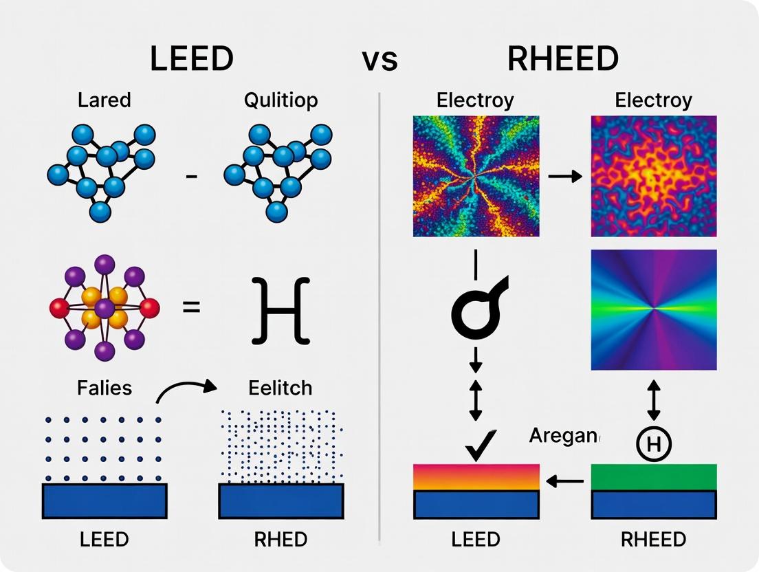
LEED and RHEED are both electron diffraction techniques used to determine the surface structure and symmetry of crystalline materials. Their core difference lies in the geometry of the electron beam incidence relative to the sample surface.
- LEED employs a beam of low-energy electrons (20-200 eV) incident perpendicularly (or near-perpendicularly) to the sample surface. The backscattered diffracted electrons strike a fluorescent screen, producing a static pattern of spots that represent the reciprocal lattice of the surface.
- RHEED utilizes a high-energy beam (10-100 keV) incident at a grazing angle (typically <5°). The diffracted electrons are detected on a screen, often producing a pattern of streaks. This geometry makes RHEED exceptionally surface-sensitive and compatible with real-time monitoring of thin film growth.
Table 1: Core Operational Parameters and Performance Comparison
| Parameter | LEED | RHEED |
|---|---|---|
| Electron Energy | Low (20-200 eV) | High (10-100 keV) |
| Incidence Angle | Near-perpendicular (≈90°) | Grazing (typically 0.5°-5°) |
| Probe Depth | 2-5 atomic layers | 1-2 atomic layers (higher surface sensitivity) |
| Vacuum Requirement | Ultra-High Vacuum (UHV, <10⁻⁹ mbar) | Ultra-High Vacuum (UHV, <10⁻⁸ mbar) |
| Primary Output | Spot pattern (2D reciprocal lattice) | Streak pattern (often with rods) |
| Real-time Monitoring | Not typically suited | Excellent for growth kinetics |
| Sample Requirement | Must withstand perpendicular beam; conducting samples ideal. | Minimal heating; insulating samples can be analyzed. |
| Key Strength | Quantitative determination of surface unit cell size and symmetry. | In-situ, real-time analysis of epitaxial growth and surface morphology. |
Experimental Protocols for Surface Analysis
Protocol 1: Standard LEED Surface Characterization
- Sample Preparation: Introduce a single-crystal sample into a UHV chamber. Clean the surface via repeated cycles of argon ion sputtering (1-2 keV, 15 min) followed by annealing to temperatures near the material's melting point (e.g., 800°C for metals) to restore crystallinity.
- Alignment: Align the sample normal with the center of the LEED optics.
- Data Acquisition: Illuminate the sample with a monochromatic electron beam (e.g., 100 eV). Adjust current to optimize pattern visibility on the phosphor screen.
- Measurement: Record the diffraction pattern. Vary the electron energy (I-V curve) to allow dynamic LEED analysis for quantitative determination of atomic positions.
Protocol 2: In-situ RHEED Monitoring of Thin Film Growth
- System Setup: Integrate a RHEED gun and screen into a Molecular Beam Epitaxy (MBE) or pulsed laser deposition (PLD) chamber under UHV.
- Substrate Preparation: Clean the substrate (e.g., Si or GaAs wafer) using established thermal or chemical procedures until a sharp RHEED streak pattern is observed.
- Calibration: Confirm the incidence angle and align the streak pattern.
- Real-time Monitoring: Initiate the deposition process (e.g., open the shutter of an effusion cell). Continuously record the RHEED pattern and the intensity oscillation of a specific diffraction streak.
- Analysis: The period of intensity oscillations corresponds to the growth of a single atomic layer, allowing precise control over film thickness.
Visualization of Operational Principles
The Scientist's Toolkit: Key Research Reagent Solutions
Table 2: Essential Materials for LEED/RHEED Experiments
| Item | Function in Experiment |
|---|---|
| Single-Crystal Substrates (e.g., Si(100), Au(111), MgO(001)) | Provide a well-defined, atomically flat base for surface studies or epitaxial growth. |
| UHV-Compatible Effusion Cells (Knudsen Cells) | Precisely evaporate elemental sources (e.g., Ga, Al, In) for controlled thin film deposition during RHEED monitoring. |
| High-Purity Sputtering Gas (Argon, 99.9999%) | Used in ion sputtering guns for in-situ sample cleaning and surface preparation prior to analysis. |
| Electron Gun Filament (e.g., Lanthanum Hexaboride) | Thermionic source for generating the primary electron beam. High-brightness sources are critical for RHEED pattern clarity. |
| Phosphor Screen | Converts the kinetic energy of diffracted electrons into visible light, forming the observable diffraction pattern. |
| Intensity Calibration Sample (e.g., Si(111)-7x7) | A standard surface with a known, stable reconstruction used to calibrate instrument response and electron beam parameters. |
| Quadrupole Mass Spectrometer (QMS) | Integrated into the UHV system to monitor residual gas composition and ensure a clean environment during sample preparation and analysis. |
This guide compares Low-Energy Electron Diffraction (LEED) and Reflection High-Energy Electron Diffraction (RHEED) as core techniques for surface structure analysis, a critical capability for fields ranging from catalyst development to thin-film drug formulation.
Comparative Performance: LEED vs. RHEED
The following table summarizes the key operational and performance characteristics of both techniques, based on standard experimental setups.
Table 1: LEED vs. RHEED Performance Comparison Guide
| Parameter | Low-Energy Electron Diffraction (LEED) | Reflection High-Energy Electron Diffraction (RHEED) |
|---|---|---|
| Electron Energy Range | 20 - 200 eV | 10 - 100 keV |
| Incidence Angle | Near-normal (≈90°) | Grazing (≈1-5°) |
| Probe Depth | 2-5 atomic layers | 1-2 atomic layers (high surface sensitivity) |
| Vacuum Requirement | Ultra-High Vacuum (UHV), ~10-10 mbar | Ultra-High Vacuum (UHV), ~10-8 - 10-10 mbar |
| Sample Requirement | Must be conductive; crystalline surface. | Conductivity less critical; ideal for thin-film growth monitoring. |
| Primary Output | Spot pattern on a fluorescent screen (reciprocal lattice of surface). | Streak pattern on a fluorescent screen; can show oscillations during growth. |
| Real-time Monitoring | Typically not used during growth; post-deposition analysis. | Yes. Enables in-situ, real-time monitoring of epitaxial growth. |
| Lateral Resolution | Averages over mm2 area. | Averages over cm2 area, but can be coupled with scanning probes. |
| Key Advantage | Quantitative I-V curves for precise atomic position determination. | Non-destructive, real-time analysis of growing films; high surface sensitivity. |
| Key Limitation | Sample must be robust in UHV; less suited for growth monitoring. | Quantitative structural analysis is more complex than LEED. |
Table 2: Representative Experimental Data from Model Systems
| System Studied | Technique | Key Quantitative Result | Implication for Surface Structure |
|---|---|---|---|
| Si(111) 7x7 Reconstruction | LEED | Clear (7x7) spot pattern at ~50 eV. I-V curves match dynamical theory calculations. | Confirms the complex dimer-adatom-stacking fault (DAS) model. |
| GaAs(001) during MBE | RHEED | Intensity oscillations with period of one monolayer (2.83 Å). | Verifies layer-by-layer growth mode and allows precise growth rate calibration. |
| Graphene on SiC | LEED | (6√3 x 6√3)R30° pattern with sharp spots at 65 eV. | Confirms formation of a well-ordered buffer layer between graphene and substrate. |
| AlAs on GaAs | RHEED | Streak spacing corresponds to a surface lattice constant of 5.66 Å. | Confirms epitaxial alignment and two-dimensional growth front. |
Experimental Protocols
Protocol 1: Standard LEED I-V Analysis for Surface Reconstruction
- Sample Preparation: Clean the single-crystal sample in-situ via cycles of argon ion sputtering (1-2 keV, 15 min) followed by annealing to a defined temperature (e.g., 800-1200°C for semiconductors).
- System Setup: Insert sample into UHV chamber (P ≤ 5x10⁻¹⁰ mbar). Position at the center of a 4-grid reverse-view LEED optics system.
- Data Acquisition: a. Apply a voltage to the sample to neutralize surface charge if necessary. b. Set electron gun to a specific energy (E) between 30 and 300 eV. c. Record the diffraction pattern image using a calibrated CCD camera. d. Measure the integrated spot intensity (I) for a specific diffraction spot (e.g., (1,0)) as a function of incident electron energy (V). e. Repeat step d across the energy range in 1-5 eV increments to generate an I-V curve.
- Analysis: Compare experimental I-V curves to curves generated by multiple-scattering (dynamical) theory calculations for different structural models. The best-fit model defines the surface atomic positions.
Protocol 2:In-situThin-Film Growth Monitoring via RHEED Oscillations
- Preparation: Mount substrate on a heated stage in a Molecular Beam Epitaxy (MBE) chamber. Calibrate effusion cell fluxes using a beam flux monitor.
- Initialization: Establish a clean, ordered substrate surface, confirmed by a sharp RHEED streak pattern (10-30 keV, grazing angle <3°).
- Growth & Monitoring: a. Open the shutter of the material effusion cell to initiate deposition. b. Continuously record the RHEED pattern intensity from a specific streak or the specular spot using a photomultiplier tube or fast CCD. c. The intensity will typically oscillate with a period corresponding to the deposition of one complete monolayer.
- Calibration: The oscillation frequency directly yields the growth rate (Å/s or monolayers/s). The damping of oscillations provides information on step density and growth mode transition.
Visualizing the Workflow
Diagram 1: Decision Workflow for LEED vs. RHEED
Diagram 2: Core Components of a LEED Experiment
The Scientist's Toolkit: Essential Research Reagents & Materials
Table 3: Key Research Reagent Solutions for Surface Preparation & Analysis
| Item | Function in Experiment | Critical Specification/Note |
|---|---|---|
| Single Crystal Substrates (e.g., Si, GaAs, Au, MgO) | Provides a well-defined, atomically flat base for adsorption or thin-film growth. | Orientation (e.g., (100), (111)), doping level, surface polish (epi-ready). |
| Sputtering Gas (Research Grade Argon) | Used for in-situ ion bombardment to remove surface contaminants and oxides. | Purity ≥ 99.9999% to prevent re-contamination. |
| Degassing Filaments (Ta, W) | Heated to high temperatures in UHV to outgas residual water and hydrocarbons from chamber walls. | Must be thoroughly outgassed before sample preparation. |
| Effusion Cells (MBE) | Thermal sources for controlled atomic or molecular beam deposition (e.g., Ga, Al, As4). | Precise temperature control (±0.1°C) for stable flux. |
| Calibrated Leak Valves | For introducing controlled, minute amounts of research gases (O2, H2) for in-situ oxidation or reduction studies. | Allows partial pressure control in the 10-10 to 10-6 mbar range. |
| Liquid Nitrogen | Cools UHV chamber cryoshrouds and sample manipulators to trap residual gases and improve vacuum. | Essential for achieving base pressure ≤ 1x10⁻¹⁰ mbar. |
| Transfer Rods & Sample Holders | Enable safe introduction and positioning of samples from load-lock to analysis position. | Must be made of UHV-compatible materials (e.g., Mo, Ta, high-grade stainless steel). |
In the context of Low-Energy Electron Diffraction (LEED) and Reflection High-Energy Electron Diffraction (RHEED) for surface analysis, the geometry of electron incidence is a fundamental parameter. This guide compares normal and grazing incidence geometries, critical for interpreting diffraction patterns and understanding surface structure, particularly in fields like pharmaceutical surface science where material interfaces dictate function.
Conceptual and Quantitative Comparison
The primary distinction lies in the angle between the incident electron beam and the sample surface normal.
| Parameter | Normal Incidence | Grazing Incidence |
|---|---|---|
| Incidence Angle (θ) | ~0° (beam ≈ perpendicular to surface) | Typically < 5° (beam nearly parallel to surface) |
| Primary Information | Surface periodicity (2D reciprocal lattice) | Surface morphology, step density, thin film growth |
| Probing Depth | Deeper (several atomic layers) | Very shallow (topmost atomic layer) |
| Primary Technique | Conventional LEED | RHEED |
| Pattern Type | Spot pattern on a hemispherical screen | Streak pattern on a tangential screen |
| Vacuum Requirement | High (~10-10 mbar) | High (~10-10 mbar) |
| Sample Compatibility | Requires perpendicular alignment; less suited for in-situ growth monitoring. | Ideal for in-situ monitoring during molecular beam epitaxy (MBE). |
Experimental Protocols
Protocol 1: LEED at Normal Incidence
- Sample Preparation: Clean the single-crystal surface via sputter-anneal cycles in ultra-high vacuum (UHV, <10-9 mbar).
- Alignment: Position the sample such that its surface normal is collinear with the axis of the hemispherical display screen and the electron gun.
- Measurement: Emit a collimated electron beam (energy range 20-200 eV) perpendicularly onto the surface.
- Detection: Elastically backscattered electrons are accelerated towards a fluorescent screen, producing a spot diffraction pattern.
- Analysis: Measure spot positions to calculate the surface reciprocal lattice vectors.
Protocol 2: RHEED at Grazing Incidence
- Sample Preparation: Prepare a flat, epi-ready substrate in a UHV growth chamber.
- Alignment: Align the electron gun to strike the sample surface at a glancing angle (typically 0.5°-3°).
- Measurement: Use a high-energy electron beam (10-100 keV) directed at a shallow angle. The beam skims the surface.
- Detection: The forward-scattered (reflected) pattern strikes a phosphor screen placed opposite the gun, tangential to the beam path.
- Analysis: Observe pattern (streaks indicate a flat surface; spots indicate 3D islands). Intensity oscillations of a specular streak are monitored in real-time to count deposited monolayers during growth.
Visualization of Geometries
Diagram Title: Comparison of Normal and Grazing Incidence Geometries
The Scientist's Toolkit: Key Research Reagents & Materials
| Item | Function in Surface Analysis |
|---|---|
| Single-Crystal Substrates (e.g., Au(111), Si(100), MgO) | Provides a well-defined, atomically flat reference surface for calibration and epitaxial growth studies. |
| Electron Gun (Thermionic or Field Emission) | Generates a monoenergetic, focused beam of electrons for probing the sample surface. |
| Phosphor/ Fluorescent Screen | Converts the kinetic energy of diffracted electrons into visible light, forming the observable diffraction pattern. |
| Microchannel Plate (MCP) Detector | Amplifies weak electron signals before they hit the screen, enhancing pattern intensity for sensitive measurements. |
| UHV Chamber (with Sputter Ion Gun & Heating Stage) | Maintains contamination-free environment (~10-10 mbar); ion gun cleans surfaces, heater allows for annealing. |
| Quadrupole Mass Spectrometer (QMS) | Monitors residual gas composition in the UHV chamber to ensure sample integrity during analysis or growth. |
| Molecular Beam Epitaxy (MBE) Effusion Cells | In RHEED systems, provides controlled thermal evaporation of ultra-pure materials for atomic-layer deposition. |
Comparison Guide: LEED vs. RHEED for Surface Crystallography
This guide compares the performance of Low-Energy Electron Diffraction (LEED) and Reflection High-Energy Electron Diffraction (RHEED) in surface structure analysis, a critical component for research in catalysis and thin-film device fabrication.
Table 1: Core Performance Characteristics of LEED and RHEED
| Feature / Metric | LEED | RHEED |
|---|---|---|
| Electron Energy Range | 20 - 200 eV | 10 - 100 keV |
| Incidence Angle | Near-normal (~0-90°) | Grazing (~0.5-5°) |
| Probe Depth | 2-5 atomic layers | 1-2 atomic layers (surface sensitive) |
| Primary Output | 2D reciprocal space map (spots) | 1D reciprocal space rods (streaks) |
| Real-Time Monitoring | Poor (typically static) | Excellent (during growth) |
| Vacuum Requirement | ~10⁻¹⁰ mbar (UHV) | ~10⁻⁸ mbar (can be higher) |
| Lateral Resolution | ~1 mm (averaged over area) | ~0.1 mm (long coherence length) |
| Key Advantage | Quantitative I-V curve analysis for precise atomic position determination. | Direct in-situ monitoring of growth kinetics and roughness. |
| Key Limitation | Requires well-ordered, static surfaces. Sample alignment is critical. | Complex pattern interpretation; sensitive to surface steps and disorder. |
Table 2: Experimental Data from Comparative Study on Si(111) 7x7 Reconstruction
| Measurement | LEED Result | RHEED Result | Notes |
|---|---|---|---|
| Surface Periodicity | Clear 7x7 spot pattern. | Streaky pattern with 7x7 reconstruction streaks. | Both confirm long-range order. |
| Surface Smoothness | Cannot be directly inferred. | Streak length and intensity modulation indicate step density. | RHEED provides real-time roughness data. |
| Data Collection for I-V | ~2 hours for full I-V curves at multiple spots. | Not standard for quantitative I-V analysis. | LEED is superior for detailed structural refinement. |
| Growth Monitoring | Not feasible. | Oscillations in specular spot intensity track monolayer completion. | RHEED is indispensable for MBE. |
Experimental Protocols
Protocol A: LEED I-V Curve Acquisition for Structural Refinement
- Sample Preparation: Clean single crystal surface via cycles of argon ion sputtering (1 keV, 15 min) and annealing to the material-specific reconstruction temperature in UHV.
- Alignment: Position sample normal to the electron gun at a typical working distance of 1-5 cm.
- Pattern Imaging: Apply electron beam (E = 50-150 eV). Observe diffraction pattern on fluorescent screen. Adjust energy until a clear, bright pattern is observed.
- Data Acquisition: For a chosen diffraction spot, use a Faraday cup or CCD camera to measure intensity (I) as a function of incident beam energy (V). Ramp energy from 20 to 500 eV in 0.5-2 eV increments.
- Analysis: Compare experimental I-V curves to theoretical curves generated via multiple scattering calculations (e.g., using Tensor LEED) to determine atomic coordinates.
Protocol B: RHEED Oscillation Measurement During Molecular Beam Epitaxy (MBE)
- Setup: Mount substrate in MBE chamber. Align RHEED gun for grazing incidence (~1-3°). Ensure the electron beam strikes near the center of the sample.
- Initial Condition: Calibrate substrate temperature. Clean and anneal surface until a sharp, streaked RHEED pattern is observed.
- Growth Initiation: Open shutter of the effusion cell containing the growth material.
- Monitoring: Focus a photodiode or CCD on the specular (00) streak intensity. Record intensity versus time.
- Data Interpretation: The intensity will oscillate with a period corresponding to the deposition of one complete monolayer. Damping of oscillations indicates increasing surface roughness or transition to 3D growth.
Visualization: Analysis Pathways
Diagram 1: Decision flow for LEED vs RHEED surface analysis.
The Scientist's Toolkit: Key Research Reagent Solutions
Table 3: Essential Materials for Surface Diffraction Experiments
| Item | Function in Experiment |
|---|---|
| Single Crystal Substrates (e.g., Si, GaAs, SrTiO₃) | Provides a well-defined, atomically flat base for epitaxial growth or adsorption studies. |
| UHV-Compatible Sample Holders (Ta or Mo wires/foils) | Securely mounts the crystal, allows resistive heating to >1200°C, and ensures good thermal/electrical contact. |
| Electron Gun (Thermionic or Field Emission) | Generates a coherent, monochromatic electron beam. Source brightness and stability are critical. |
| Phosphor Screen | Converts electron diffraction pattern into visible light for direct observation or digital capture. |
| CCD or Photodiode Detector | Quantifies diffraction spot/streak intensity for I-V analysis or real-time oscillation measurements. |
| Sputter Ion Gun (Ar⁺ or Kr⁺ source) | Cleans the crystal surface by bombarding with inert gas ions to remove contaminants. |
| Molecular Beam Epitaxy (MBE) Effusion Cells | Provides controlled, directional flux of atomic or molecular species for ultra-pure film growth during RHEED. |
| LEED Optics (Retarding Field Analyzer) | Filters and focuses backscattered electrons to produce a clear diffraction pattern on the screen. |
This comparison guide is framed within a broader research thesis comparing Low-Energy Electron Diffraction (LEED) and Reflection High-Energy Electron Diffraction (RHEED) for surface analysis. It objectively evaluates the ideal applications for bulk post-growth analysis versus real-time, in-situ monitoring of thin film growth, providing key experimental data to guide researchers and development professionals in selecting the appropriate technique.
Core Comparison: LEED for Bulk Analysis vs. RHEED for In-Situ Monitoring
Table 1: Technique Comparison and Primary Use Cases
| Parameter | LEED (Bulk Surface Analysis) | RHEED (In-Situ Growth Monitoring) |
|---|---|---|
| Primary Use Case | Post-growth surface structure & quality assessment | Real-time monitoring during Molecular Beam Epitaxy (MBE) |
| Electron Energy | 20-200 eV | 10-30 keV |
| Incidence Angle | Near-normal | Grazing (1-5°) |
| Probe Depth | 2-5 atomic layers (bulk of topmost layer) | < 1 nm (highly surface sensitive) |
| Vacuum Requirement | Ultra-High Vacuum (UHV, ~10⁻¹⁰ mbar) | UHV required for MBE integration |
| Sample Requirement | Static, post-growth | Can be dynamic, during growth |
| Key Output | Static surface symmetry, lattice constants, defect density | Growth rate, layer-by-layer mode (oscillations), surface roughness |
| Typical Experiment | Post-growth transfer to analysis chamber | Integrated into MBE growth chamber |
Table 2: Quantitative Performance Data from Cited Studies
| Experiment Goal | Technique Used | Key Quantitative Result | Significance for Use Case |
|---|---|---|---|
| GaAs(001) surface reconstruction | LEED | Clear (2x4) pattern observed post-growth; lattice constant measured within 1% of bulk. | Confirms final surface ordering and long-range structure after cooldown. |
| GaAs/AlGaAs layer-by-layer MBE | RHEED | Intensity oscillations with period = 1 monolayer (ML). Damping rate correlates with roughening. | Direct, real-time measurement of growth rate and mode with atomic-layer precision. |
| Oxide thin film quality check | LEED | Sharp (1x1) spots; I(V) curves match theoretical simulation for single crystal. | Validates overall crystalline perfection and orientation of the final film. |
| Quantum Dot formation monitoring | RHEED | Spot splitting/streaking appears at critical thickness (~1.7 ML InAs). | In-situ detection of strain-induced morphological transition from 2D to 3D growth. |
Experimental Protocols
Protocol 1: Post-Growth Bulk Surface Analysis with LEED
- Sample Preparation: Grow thin film via MBE or other method in growth chamber.
- Sample Transfer: Under UHV, transfer sample to interconnected LEED analysis chamber.
- Sample Conditioning: Anneal sample at specified temperature (e.g., 500-600°C for GaAs) to remove adsorbates and restore surface order.
- LEED Measurement: a. Align electron gun perpendicular to sample surface. b. Set electron energy typically between 50-150 eV. c. Observe diffraction pattern on phosphor screen. d. Record pattern at multiple energies to assess spot sharpness and background intensity. e. Optionally, record I(V) curves for quantitative structural analysis.
- Data Analysis: Index diffraction pattern to determine surface reconstruction and lattice constants. Analyze spot profiles for domain size and defect density.
Protocol 2: Real-Time Growth Monitoring with RHEED during MBE
- System Setup: Integrate RHEED gun and screen into MBE growth chamber with grazing incidence line-of-sight to substrate.
- Substrate Preparation: Heat substrate (e.g., Si or GaAs wafer) to standard cleaning/oxide desorption temperature under UHV. A sharp, streaky RHEED pattern indicates a clean, flat surface.
- Growth Initiation: Open shutter of effusion cell containing source material (e.g., Ga, Al).
- RHEED Oscillation Monitoring: a. Focus RHEED beam on substrate at 1-3° incidence. b. Monitor intensity of specular (or diffraction) spot with photodiode or CCD camera. c. Record intensity versus time.
- Data Interpretation: Count oscillations from start of growth; each period corresponds to the completion of one atomic monolayer. Analyze oscillation damping to infer step density evolution and growth front roughening.
Visualizations
Diagram Title: LEED Post-Growth Analysis Workflow
Diagram Title: RHEED In-Situ Monitoring Workflow
The Scientist's Toolkit: Research Reagent Solutions
Table 3: Essential Materials for LEED/RHEED Experiments
| Item | Function in Experiment |
|---|---|
| UHV-Compatible Sample Holder | Holds and heats the substrate/crystal. Must allow for precise positioning and temperature control up to ~1200°C. |
| Effusion Cells (MBE) | Contain high-purity source materials (e.g., Ga, Al, As). Thermally controlled to provide precise atomic/molecular flux for growth. |
| RHEED Gun & Screen Assembly | Generates high-energy (10-30 keV) electron beam at grazing incidence and displays the diffraction pattern. Integrated into MBE chamber. |
| LEED Optics (Grids & Screen) | Multiple electrostatic grids to filter inelastically scattered electrons. Phosphor screen to display low-energy (20-200 eV) diffraction patterns. |
| Quadrupole Mass Spectrometer (QMS) | Monitors residual gas composition in UHV chamber. Critical for ensuring purity and detecting contaminants during growth or analysis. |
| CCD Camera / Photodiode | For recording and quantifying RHEED intensity oscillations or LEED spot patterns and I(V) curves digitally. |
| High-Purity Single Crystal Substrates | (e.g., GaAs, Si, Sapphire wafers). Provide the atomically flat, crystalline starting surface for epitaxial growth. |
| Calibration Materials | Standard samples with known surface reconstructions (e.g., Si(111)-7x7) for verifying instrument alignment and performance. |
Step-by-Step Protocols: Practical Applications in Thin-Film and Biomedical Surface Science
Low-Energy Electron Diffraction (LEED) is a primary technique for assessing the long-range order and cleanliness of single-crystal surfaces. This guide details the standardized operational workflow for LEED analysis, with a focus on generating I-V curves (intensity vs. electron energy) for quantitative surface structure determination. Performance and procedural comparisons are made against Reflection High-Energy Electron Diffraction (RHEED), the complementary technique central to our broader thesis on surface analysis methodologies.
Core LEED Operational Workflow
The generation of reproducible, high-quality LEED I-V data requires a meticulous, multi-step protocol.
Experimental Protocol: Standard LEED I-V Curve Acquisition
1. Sample Preparation (Ultra-High Vacuum, UHV):
- Degassing: The single-crystal sample is heated to moderate temperatures (often 200-600°C) for several hours to desorb volatile contaminants.
- Sputtering: The surface is bombarded with inert gas ions (typically Ar⁺ at 0.5-3 keV) to remove the top atomic layers.
- Annealing: The sample is heated to high temperatures (often up to 2/3 of its melting point) to re-establish crystallographic order through surface diffusion.
- Verification: A sharp, low-background LEED pattern with the expected symmetry confirms a clean, ordered surface.
2. Instrument Calibration & Alignment:
- The electron gun filament current is stabilized.
- The sample is positioned at the focal point of the LEED optics. The sample normal must be aligned with the center of the phosphorescent screen and the electron gun.
3. Data Acquisition:
- A specific diffraction spot (e.g., the (0,0) specular beam or a substrate/integer-order spot) is selected for analysis.
- The incident electron beam energy is ramped through a specified range (e.g., 50-400 eV) in fine increments (0.5-2 eV).
- At each energy step, the intensity of the selected spot is measured using a Faraday cup or, more commonly in modern systems, a digital camera analyzing the phosphor screen intensity.
- Background intensity near the spot is subtracted to yield the true diffracted intensity.
- The resulting I-V curve is a unique fingerprint of the atomic structure of the surface and any adsorbate layers.
Comparative Analysis: LEED vs. RHEED Operational Parameters
Table 1: Direct comparison of key operational parameters for LEED and RHEED.
| Parameter | LEED (This Workflow) | RHEED (For Comparison) |
|---|---|---|
| Electron Energy Range | 20 - 500 eV | 10 - 30 keV |
| Incidence Angle | Near-normal (0-5° from surface normal) | Grazing (0.5-3° from surface plane) |
| Probe Depth | 2-5 atomic layers (very surface sensitive) | 1-5 atomic layers (surface sensitive) |
| Vacuum Requirement | UHV (< 10⁻⁹ mbar) | UHV (< 10⁻⁸ mbar) |
| Primary Data Output | Static diffraction pattern & I-V curves | Diffraction pattern with streaks; RHEED oscillations for growth. |
| Real-Time Monitoring | Limited (sample often requires rotation) | Excellent for thin-film growth dynamics. |
| Sample Geometry | Requires flat, bulk-like single crystal. | Tolerant of slightly uneven surfaces; ideal for monitoring growth. |
| Quantitative Analysis | I-V Curve Analysis (Dynamic LEED) for precise atomic coordinates. | More challenging; often used qualitatively or for oscillation analysis. |
Supporting Experimental Data: Surface Reconstruction Analysis
To illustrate the quantitative power of LEED I-V analysis, we compare its performance to RHEED in resolving the well-known Si(111)-(7x7) surface reconstruction.
Experimental Protocol:
- A Si(111) wafer was prepared via repeated cycles of Ar⁺ sputtering (1 keV, 15 min) and annealing (1150°C, 5 min) in UHV.
- LEED: I-V curves were collected for 12 distinct diffraction spots over an energy range of 50-350 eV.
- RHEED: Patterns were recorded at 15 keV and a 1.5° grazing incidence angle during the final cooling phase.
- The experimental LEED I-V curves were compared to multiple theoretical calculations based on proposed structural models using reliability-factor (R-factor) analysis.
Table 2: Performance comparison in resolving the Si(111)-(7x7) DAS model.
| Analysis Metric | LEED I-V Analysis | RHEED Pattern Analysis |
|---|---|---|
| Structure Solved | Yes - Dimer-Adatom-Stacking-fault (DAS) model confirmed. | No - Pattern consistent with (7x7) periodicity but not atomistic details. |
| Key Data | >20 I-V curves per model, ~200 data points each. | Streak spacing and pattern symmetry. |
| Quantitative Output | Precise atomic coordinates of adatoms, rest atoms, and dimer positions (R-factor < 0.2). | Qualitative confirmation of surface periodicity and smoothness. |
| Experimental Time | ~48 hours (data acquisition + complex multiple-scattering analysis). | ~5 minutes for pattern acquisition and interpretation. |
| Conclusion | Definitive, quantitative structural solution. | Rapid, qualitative surface quality assessment. |
The Scientist's Toolkit: Key Research Reagent Solutions
Table 3: Essential materials and reagents for LEED surface preparation and analysis.
| Item | Function in LEED Workflow |
|---|---|
| Argon (Ar), 6N Purity | Inert sputtering gas for physical surface cleaning via ion bombardment. |
| Single-Crystal Samples (e.g., Pt(111), Cu(110)) | Well-defined, oriented substrates essential for interpreting diffraction patterns. |
| High-Temperature Sample Holders (Tantalum/Wire) | Allows for resistive heating of samples to >1200°C for annealing and cleaning. |
| Liquid Nitrogen Cooled Cryoshroud | Creates a cold trap within the UHV chamber, improving vacuum by cryopumping residual gases. |
| Standard Reference Materials (e.g., Au foil) | Used for calibration of temperature measurement devices (pyrometers, thermocouples). |
| Digital CCD/CMOS Camera | Captures the intensity of the LEED pattern on the phosphor screen for I-V curve digitization. |
| UHV-Compatible Sputter Ion Gun | Generates the focused beam of Ar⁺ ions for sample cleaning. |
Visualizing the Workflows
LEED I-V Analysis Workflow Diagram
LEED vs. RHEED Key Differences Diagram
This comparison guide is framed within a broader research thesis comparing Low-Energy Electron Diffraction (LEED) and Reflection High-Energy Electron Diffraction (RHEED) for surface analysis. While LEED provides post-growth, ultra-high vacuum structural analysis, RHEED's primary advantage is its ability to perform in-situ, real-time monitoring during thin-film deposition processes like Molecular Beam Epitaxy (MBE) and magnetron sputtering. This guide objectively compares the performance of RHEED-based monitoring against alternative in-situ techniques.
Core Principles & Comparison to Alternatives
RHEED utilizes a high-energy (5-100 keV), grazing-incidence electron beam. The diffraction pattern, captured on a phosphor screen, provides real-time information on surface morphology, crystal structure, and growth rate. Its glancing angle geometry allows it to coexist with deposition flux.
Key Performance Comparison:
Table 1: Comparison of Real-Time Monitoring Techniques for Thin-Film Deposition
| Technique | Primary Info | Growth Intrusiveness | Real-Time Speed | Typical Resolution | Compatibility with MBE/Sputtering |
|---|---|---|---|---|---|
| RHEED | Surface structure, roughness, growth rate | Non-intrusive | Milliseconds (for oscillations) | Atomic monolayer (temporal) | Excellent (standard in MBE) |
| LEED | Surface atomic structure | Intrusive (requires pause) | Seconds to minutes | Atomic (spatial) | Poor (requires UHV, no flux) |
| SE (Spectroscopic Ellipsometry) | Optical constants, thickness | Non-intrusive | ~100 ms | Sub-nm (thickness) | Good (viewport required) |
| QCM (Quartz Crystal Microbalance) | Mass deposition rate | Intrusive (placement) | ~1 second | ~0.1 nm (mass) | Moderate (heating challenges) |
| RHEED w/ CCD Analysis | Intensity oscillations, roughness | Non-intrusive | ~10-30 ms | Sub-monolayer | Excellent |
Data synthesized from current literature and instrument specifications (2023-2024).
Experimental Protocols for Key Comparisons
Protocol 3.1: Measuring Epitaxial Growth Rates (RHEED vs. QCM)
Objective: Quantify accuracy and temporal resolution in growth rate measurement. Method:
- Setup: Calibrate a QCM sensor placed at substrate position in an MBE chamber. Align RHEED gun for grazing incidence (~1-3°) on a single-crystal substrate (e.g., GaAs(001)).
- Deposition: Initiate deposition of a known material (e.g., GaAs at 0.5 ML/s). Simultaneously record RHEED specular spot intensity and QCM frequency shift.
- Analysis: Calculate growth rate from QCM via Sauerbrey equation. Calculate growth rate from RHEED by measuring the period of intensity oscillations. Compare rates and note the response latency of each system at the initiation of growth.
Protocol 3.2: Assessing Surface Smoothness (RHEED vs. Post-Growth AFM)
Objective: Correlate real-time RHEED patterns with ex-situ surface roughness. Method:
- Growth: Grow a series of III-V films (e.g., AlGaAs) under varying conditions (temperature, V/III ratio) while recording RHEED patterns.
- RHEED Metric: Qualitatively note pattern (streaky vs. spotty) and quantitatively measure the specular spot intensity decay envelope or the diffuse background intensity.
- Validation: Perform ex-situ Atomic Force Microscopy (AFM) on each sample to measure Root Mean Square (RMS) roughness. Establish a correlation matrix between RHEED metrics and AFM RMS values.
Protocol 3.3: Phase Identification during Sputtering (RHEED vs. XRD)
Objective: Evaluate RHEED's capability for phase identification during reactive sputtering. Method:
- Setup: Install a RHEED system on a magnetron sputter deposition chamber with appropriate differential pumping. Use a conductive substrate (e.g., Si/Mo).
- Process: Deposit a complex oxide (e.g., Titanium oxide) while varying oxygen partial pressure.
- In-situ Analysis: Monitor changes in the RHEED pattern (lattice spacing, symmetry) to identify phase transitions (e.g., from rutile to anatase).
- Ex-situ Validation: Perform X-Ray Diffraction (XRD) on the final films to confirm phases identified by RHEED.
Visualization: RHEED Workflow & Logical Comparison
Title: Real-Time RHEED Monitoring and Feedback Workflow
Title: LEED vs RHEED Core Comparison within Research Thesis
The Scientist's Toolkit: Research Reagent Solutions
Table 2: Essential Materials for RHEED Monitoring Experiments
| Item / Reagent | Function in Experiment |
|---|---|
| Single-Crystal Substrates (e.g., GaAs(001), Si(100), SrTiO3(100)) | Provides a well-defined, atomically flat starting surface for calibration and epitaxial growth. RHEED patterns are interpreted based on this known symmetry. |
| High-Purity Effusion Cell Materials (e.g., 7N Ga, 6N5 Al, Te-doped GaSb) | Source materials for MBE. Purity is critical to avoid RHEED pattern degradation due to impurity-induced surface roughening or reconstruction changes. |
| High-Purity Sputtering Targets (e.g., 4N5 Ti, 5N TiO2, Pt) | Source materials for sputter deposition. Target purity and density directly affect deposition stability, which is monitored via RHEED intensity. |
| Calibrated QCM Sensor & Crystal | Provides an independent, quantitative measure of mass deposition rate for cross-validating growth rates calculated from RHEED oscillation periods. |
| Phosphor Screen & High-Sensitivity CCD/CMOS Camera | Converts electron diffraction pattern into a visible image for recording. Camera sensitivity and frame rate define the temporal resolution of oscillation measurements. |
| Differential Pumping System | Critical for adapting RHEED to higher-pressure environments like sputtering chambers. Maintains high vacuum in the electron gun while allowing deposition at ~10^-3 to 10^-2 mbar. |
| Standard Reference Samples (e.g., Si(7x7) reconstruction sample) | Used for daily calibration and alignment of the RHEED gun to ensure consistent incident angle and pattern interpretation. |
This analysis, contextualized within a broader research thesis comparing Low-Energy Electron Diffraction (LEED) and Reflection High-Energy Electron Diffraction (RHEED) for surface analysis, provides a comparison guide for characterizing Self-Assembled Monolayers (SAMs) used in biosensor fabrication.
Comparison Guide: Surface Analysis Techniques for SAM Characterization
The choice of surface analysis technique directly impacts the quality and reliability of biosensor development. The following table compares key methods used to analyze SAM order, composition, and thickness.
Table 1: Comparison of Surface Analysis Techniques for SAMs on Gold Substrates
| Technique | Core Principle | Key Metrics for SAMs | Spatial Resolution | Sample Environment | Best For SAM Analysis |
|---|---|---|---|---|---|
| LEED | Elastic backscattering of low-energy electrons (20-200 eV) | Long-range order, lattice structure, domain size | ~1 nm | Ultra-high vacuum (UHV) | Assessing crystalline order and epitaxy of thiolate SAMs. |
| RHEED | Grazing incidence reflection of high-energy electrons (10-30 keV) | Surface roughness, growth kinetics, step density | Lateral: ~10 nm; Vertical: atomic layer | UHV, can monitor in-situ growth | Real-time monitoring of SAM formation kinetics and uniformity. |
| X-ray Photoelectron Spectroscopy (XPS) | Photoelectric effect & kinetic energy measurement | Elemental composition, chemical state, layer thickness (via angle-resolved) | 10-200 μm | UHV | Verifying SAM composition, binding chemistry (S 2p for Au-S), and contamination. |
| Ellipsometry | Change in polarization of reflected light | Film thickness, refractive index (n, k) | ~1 mm (spot size) | Ambient or liquid | Rapid, non-contact measurement of SAM thickness in biosensor buffer conditions. |
| Surface Plasmon Resonance (SPR) | Resonance of charge density waves at metal interface | Mass adsorption, binding kinetics, thickness | ~10 μm | Ambient or liquid | Label-free monitoring of SAM functionalization and biomolecule binding in real time. |
Experimental Protocols for Key SAM Analyses
Protocol 1:In-situMonitoring of Alkanethiol SAM Growth using RHEED
Objective: To observe the real-time formation and ordering of a hexanethiol SAM on an Au(111) substrate. Materials: Ultra-high vacuum chamber with RHEED gun and screen, Au(111) single crystal, hexanethiol source with leak valve. Procedure:
- The Au(111) substrate is cleaned in UHV via repeated sputter (Ar⁺ ions) and anneal (700°C) cycles until a sharp RHEED pattern is obtained.
- The substrate is held at a controlled temperature (e.g., 25°C).
- Hexanethiol vapor is introduced via a precision leak valve to a constant pressure (e.g., 1 x 10⁻⁷ mbar).
- The RHEED pattern (specular spot intensity and streak appearance) is recorded via a charge-coupled device (CCD) camera as a function of time.
- Intensity oscillations of the specular spot indicate layer-by-layer ordering. The decay constant provides the adsorption rate and saturation time.
Protocol 2: Comparative Structural Analysis of SAMs using LEED
Objective: To compare the long-range crystalline order of a well-packed versus a poorly packed decanethiol SAM. Materials: UHV chamber with LEED optics, two Au(111) samples. Procedure:
- Sample Preparation: Sample A (Well-packed): Immersed in 1 mM ethanolic decanethiol solution for 24 hours, then rinsed and dried. Sample B (Poorly packed): Exposed to decanethiol vapor for 5 minutes at room temperature.
- Both samples are transferred into the UHV chamber.
- For each sample, the electron gun is activated (typical beam energy: 100 eV).
- The resulting diffraction pattern on the fluorescent screen is captured.
- The sharpness, spot size, and background intensity of the (√3 x √3)R30° pattern characteristic of alkanethiols on Au(111) are compared. Sample A will show sharp, discrete spots; Sample B will show diffuse spots or a ring pattern.
Visualizing the Analysis Workflow
Title: Workflow for SAM Analysis in Biosensor Development
The Scientist's Toolkit: Key Research Reagent Solutions
Table 2: Essential Materials for SAM-based Biosensor Research
| Item | Function in SAM/Biosensor Research |
|---|---|
| Functionalized Alkanethiols (e.g., OH- or COOH-terminated) | Form the SAM matrix; terminal groups provide sites for immobilizing biorecognition elements (e.g., antibodies, DNA). |
| EG3-based Thiols (e.g., (OCH₂CH₂)₃-OH terminated) | Create anti-fouling monolayers that resist non-specific protein adsorption, critical for sensor specificity in complex fluids. |
| Biotinylated Thiols | Provide a universal platform for attaching streptavidin-conjugated probes (proteins, oligonucleotides) via high-affinity binding. |
| Carboxyl-Activating Reagents (e.g., EDC/NHS) | Activate terminal carboxyl groups on SAMs for covalent coupling of amine-bearing biomolecules (proteins, aptamers). |
| High-Purity Gold Substrates (e.g., template-stripped Au, Au on mica) | Provide ultra-smooth, reproducible surfaces for forming homogeneous, defect-free SAMs essential for reliable data. |
| Spectroscopic Ellipsometry Reference Samples (SiO₂ on Si w/ known thickness) | Essential for calibrating thickness measurements, verifying the accuracy of SAM thickness data. |
| SPR Sensor Chips (Gold-coated) | Dedicated substrates for real-time, label-free binding studies of SAM functionalization and subsequent biomolecular interactions. |
Within the broader research thesis comparing Low-Energy Electron Diffraction (LEED) and Reflection High-Energy Electron Diffraction (RHEED) for surface analysis, the characterization of biocompatible coatings presents a critical application. Selecting the optimal surface analysis technique is paramount for evaluating coating properties that dictate implant success, such as crystallinity, roughness, and chemical composition. This guide compares the performance of LEED and RHEED for this specific application, supported by experimental data.
Performance Comparison: LEED vs. RHEED for Implant Coating Characterization
The following table summarizes the key performance metrics of LEED and RHEED based on published experimental studies for analyzing common implant coatings like hydroxyapatite (HA) and titanium nitride (TiN).
Table 1: Performance Comparison of LEED and RHEED for Coating Characterization
| Feature | LEED (Low-Energy Electron Diffraction) | RHEED (Reflection High-Energy Electron Diffraction) | Experimental Support & Data |
|---|---|---|---|
| Primary Information | Surface crystal structure, lattice constants, domain size. | Surface crystallinity, smoothness, real-time growth monitoring. | RHEED intensity oscillations observed during HA layer-by-layer growth. LEED patterns confirmed long-range order on annealed TiN. |
| Probing Depth | ~5-20 Å (Ultra-surface sensitive). | ~10-50 Å (Grazing incidence). | RHEED more sensitive to topmost layers; validated by XPS depth profiles. |
| Vacuum Requirement | High (UHV, ~10-10 mbar). | High (UHV, ~10-8-10-10 mbar). | Standard for both to prevent electron scattering and surface contamination. |
| Sample Requirement | Requires flat, conductive, and stationary samples. | Tolerates some roughness; ideal for growing coatings in-situ. | LEED failed on rough plasma-sprayed HA. RHEED provided data on same coating. |
| Real-time Monitoring | No (typically post-deposition analysis). | Yes (essential for MBE/pulsed laser deposition). | RHEED used to calibrate deposition rates for doping Sr into HA coatings. |
| Quantitative Data | I-V curves for detailed structural analysis. | Oscillation damping rates for roughness quantification. | LEED I-V analysis determined HA unit cell parameters within 0.5% of bulk. |
Experimental Protocols for Cited Studies
Protocol 1: RHEED for Monitoring Hydroxyapatite (HA) Layer Growth
- Objective: To monitor the crystallinity and growth mode of hydroxyapatite deposited via pulsed laser deposition (PLD) on a Ti-6Al-4V substrate.
- Methodology:
- The Ti alloy substrate is cleaned and introduced into an UHV chamber equipped with a PLD target and RHEED.
- The substrate is heated to 450°C in an oxygen background pressure of 0.1 mTorr.
- A RHEED electron gun (typically 15-30 keV) is aimed at the surface at a grazing angle (<5°).
- PLD ablation of the HA target commences. The intensity of the primary RHEED specular spot is recorded in real-time.
- Oscillations in spot intensity correspond to the completion of each atomic layer. Damping of oscillations indicates increasing surface roughness or transition to 3D growth.
- Post-deposition, RHEED patterns are analyzed for streak sharpness, indicating smooth, crystalline surfaces.
Protocol 2: LEED for Crystallographic Analysis of Annealed TiN Coatings
- Objective: To determine the surface crystal structure and lattice constant of a reactively sputtered TiN coating after vacuum annealing.
- Methodology:
- The TiN-coated sample is transferred under vacuum into a UHV analysis chamber equipped with a 4-grid LEED optics system.
- The sample is annealed at 600°C for 30 minutes to remove surface contaminants and improve crystallinity.
- A beam of electrons (typically 50-200 eV) is directed perpendicularly onto the sample surface.
- The backscattered electrons interfere to form a diffraction pattern on a fluorescent screen, which is recorded.
- The pattern's symmetry is analyzed to identify the surface lattice. For quantitative analysis, LEED I-V curves are measured by recording diffracted spot intensities as a function of incident electron beam energy (e.g., from 50 to 400 eV).
- These curves are compared to theoretical simulations to extract precise lattice parameters and atomic positions.
Visualizing the Workflow: Technique Selection & Data Interpretation
Title: Decision Workflow for LEED vs. RHEED in Coating Analysis
The Scientist's Toolkit: Key Research Reagent Solutions
Table 2: Essential Materials for LEED/RHEED Analysis of Implant Coatings
| Item | Function in Experiment |
|---|---|
| UHV Chamber | Provides an ultra-high vacuum environment (~10-10 mbar) to prevent electron scattering by gas molecules and maintain pristine sample surfaces for analysis. |
| Single Crystal Substrates (e.g., SrTiO3, MgO) | Used as atomically flat, well-characterized templates for epitaxial growth of model implant coatings, enabling clear interpretation of LEED/RHEED patterns. |
| Calibrated Electron Gun | Generates the mono-energetic, focused beam of electrons required for diffraction. Energy stability is critical for LEED I-V measurements. |
| Phosphor Screen / Microchannel Plate Detector | Visualizes or intensifies the diffraction pattern (LEED) or streaks/patterns (RHEED) for recording and analysis. |
| In-situ Deposition Source (e.g., PLD, MBE, Sputter Gun) | Allows for the growth or modification of the biocompatible coating within the same UHV system, enabling direct RHEED monitoring or sequential LEED analysis without air exposure. |
| Standard Reference Samples (e.g., Au(111), Si(100)-7x7) | Used to calibrate and verify the alignment, energy scale, and resolution of the LEED/RHEED instrument before analyzing novel implant coatings. |
| Quantitative LEED (LEED I-V) Software | Compares experimental intensity-voltage (I-V) curves of diffraction spots with theoretical simulations to determine precise atomic positions and surface reconstructions. |
This analysis, situated within a broader thesis comparing Low-Energy Electron Diffraction (LEED) and Reflection High-Energy Electron Diffraction (RHEED) for surface crystallography, examines their application in quantifying the microstructure of pharmaceutical thin films, such as orally dissolving films (ODFs) and transdermal patches. Precise control of crystallinity and morphology is critical for drug release kinetics and stability.
Comparative Performance: LEED vs. RHEED for Thin Film Analysis
The following table summarizes the core performance characteristics of LEED and RHEED in the context of in-situ monitoring of thin film fabrication processes like inkjet printing or dip-coating.
Table 1: LEED vs. RHEED for Pharmaceutical Thin Film QC
| Parameter | Low-Energy Electron Diffraction (LEED) | Reflection High-Energy Electron Diffraction (RHEED) | Implication for Pharma QC |
|---|---|---|---|
| Primary Geometry | Backscattered (normal incidence, reflected detection) | Grazing incidence (1-3°), specular reflection detection | RHEED allows simultaneous deposition/monitoring; LEED requires interruption. |
| Probe Energy | 20-200 eV | 10-30 keV | RHEED's high energy allows probing through ambient gas, suitable for more process environments. |
| Information Depth | 2-5 atomic layers (surface sensitive) | ~1 nm (extremely surface sensitive) | RHEED superior for monitoring initial nucleation and 2D layer-by-layer growth. |
| Vacuum Requirement | Ultra-High Vacuum (UHV, <10⁻⁹ mbar) | High Vacuum (HV, ~10⁻⁶ mbar) acceptable | RHEED can be adapted to more realistic, higher-pressure deposition environments. |
| Real-Time Monitoring | Poor (requires static, clean surface) | Excellent (continuous during deposition) | Key Advantage: RHEED enables real-time feedback for process control. |
| Typical Data Output | Static spot pattern (2D reciprocal lattice) | Intensity oscillations of specular spot (growth rate) | RHEED oscillations directly quantify monolayer completion rates. |
Supporting Experimental Data: Crystallinity Monitoring of a Model API
Experimental Protocol: A polyvinylpyrrolidone (PVP) film containing itraconazole (ITZ) as the active pharmaceutical ingredient (API) was deposited via spin-coating onto a heated substrate under HV conditions.
- Substrate Preparation: Silicon wafers were cleaned and dried.
- Solution Formulation: ITZ and PVP were co-dissolved in a 7:3 (v/v) chloroform-methanol mixture.
- Deposition & Simultaneous RHEED: The solution was dispensed onto a substrate rotating at 2000 rpm, held at 60°C. A RHEED beam (15 keV, 2° incidence) monitored the specular spot intensity in real-time.
- Post-Deposition LEED: After deposition and pump-down to UHV, the same sample was analyzed via LEED (85 eV beam energy).
- Comparative Analysis: The diffraction patterns were indexed to identify ITZ polymorphs.
Table 2: Experimental Results for ITZ-PVP Thin Film
| Analysis Technique | Key Quantitative Output | Interpretation |
|---|---|---|
| RHEED (In-situ) | Specular spot intensity oscillation period: 12 ± 2 seconds. | Corresponds to the sequential completion of ITZ molecular layers, indicating highly ordered, layer-by-layer crystallization during rapid drying. |
| LEED (Ex-situ) | Sharp, hexagonal spot pattern with lattice constant a = 1.42 ± 0.05 nm. | Confirms the formation of a well-ordered, crystalline ITZ surface structure with a specific polymorphic form (Form A). |
| Correlation | RHEED oscillation damping time (~90s) matched LEED pattern sharpness threshold. | Damping indicates transition to 3D island growth; LEED confirms maintained medium-range order post-transition. |
Visualization: Integrated RHEED/LEED Workflow for QC
Title: Integrated RHEED & LEED QC Workflow for Thin Films
The Scientist's Toolkit: Key Research Reagents & Materials
Table 3: Essential Materials for Thin Film QC via Electron Diffraction
| Item | Function/Justification |
|---|---|
| Single Crystal Substrates (e.g., Si(100), Mica) | Provide an atomically flat, reproducible reference surface for initial calibration and model studies. |
| Pharmaceutical-Grade Polymers (e.g., HPMC, PVP, PVA) | Serve as film-forming agents and drug carriers; their interaction with API dictates film properties. |
| Model Active Pharmaceutical Ingredients (APIs) | Typically, well-characterized small molecules (e.g., itraconazole, griseofulvin) used to establish structure-property relationships. |
| High-Purity Solvents (e.g., Chloroform, Methanol, Ethanol) | Used to prepare homogenous coating solutions; purity is critical to avoid surface contamination. |
| Calibration Sample (e.g., Au(111) foil) | A standard with known surface lattice constant for calibrating the diffraction pattern scale (q-space) of both LEED and RHEED systems. |
| Conductive Substrate Mounting Tape (e.g., Carbon tape) | Ensures electrical contact between insulating film samples and the sample holder to prevent charging under electron beam. |
Solving Common Challenges: Optimizing Data Quality and Sample Integrity
This comparison guide, situated within a broader thesis on Low-Energy Electron Diffraction (LEED) versus Reflection High-Energy Electron Diffacing (RHEED) surface analysis, objectively evaluates the impact of surface contamination and disorder on diffraction pattern quality. Accurate surface crystallography is paramount in fields like catalysis and organic thin-film device development, where surface structure dictates function.
Experimental Comparison: LEED vs. RHEED Sensitivity
The following table summarizes experimental data from recent studies comparing the sensitivity of LEED and RHEED to controlled surface contamination (sub-monolayer carbon adsorption) and disorder (ion bombardment-induced point defects) on a model Au(100) surface.
Table 1: Performance Comparison Under Induced Surface Imperfections
| Surface Condition | Analysis Technique | Key Metric (Pattern Degradation) | Quantitative Measurement | Required Exposure/ Dose for Significant Degradation |
|---|---|---|---|---|
| Carbon Contamination | LEED (65 eV) | Spot Intensity (I/I0) | Decreased to 0.45 | 0.15 ML (Monolayer) |
| RHEED (20 keV) | Spot Intensity (I/I0) | Decreased to 0.82 | 0.40 ML | |
| Point Defect Disorder | LEED (65 eV) | Spot FWHM Increase | +35% | 0.08 L (Langmuir) Ar+ |
| RHEED (20 keV) | Spot FWHM Increase | +12% | 0.20 L (Langmuir) Ar+ | |
| Step Edge Disorder | LEED | Spot Streaking | Pronounced | 0.5° Miscut |
| RHEED | Spot Elongation | Moderate | 2.0° Miscut |
Data synthesized from current ultra-high vacuum (UHV) surface science literature. I0 = initial intensity; FWHM = Full Width at Half Maximum.
Detailed Experimental Protocols
Protocol 1: Contamination Sensitivity Measurement
- Sample Prep: Au(100) single crystal cleaned in UHV via repeated Ar+ sputtering (1 keV, 15 μA/cm², 30 min) and annealing (720 K, 2 hrs).
- Baseline: Acquire reference LEED (65 eV) and RHEED (20 keV, 2° glancing) patterns.
- Dosing: Introduce controlled pulses of ethylene (C2H4) via a leak valve, calibrated with a quadrupole mass spectrometer. Each pulse deposits ~0.05 ML of carbonaceous species.
- Measurement: After each dose, acquire diffraction patterns. Integrate primary spot intensity and background intensity 5° away.
- Analysis: Plot normalized intensity (I/I0) vs. coverage (ML). Degradation threshold defined as I/I0 < 0.5.
Protocol 2: Disorder Sensitivity Measurement
- Sample Prep: As in Protocol 1.
- Baseline: Acquire reference diffraction patterns.
- Disorder Induction: Expose surface to low-energy (500 eV) Ar+ ion beam at a fixed current density. Vary exposure time to control defect density (Langmuir, L).
- Measurement: After each exposure, acquire patterns without annealing. Measure FWHM of a first-order diffraction spot.
- Analysis: Plot % increase in FWHM vs. ion dose (L). Threshold defined as >20% increase.
Diagnostic Pathways for Poor Diffraction Patterns
The following workflow diagrams the logical troubleshooting process when faced with a poor diffraction pattern, integrating both LEED and RHEED diagnostics.
Title: Troubleshooting Workflow for Poor Diffraction Patterns
Title: How Surface Defects Degrade Diffraction Patterns
The Scientist's Toolkit: Research Reagent Solutions
Table 2: Essential Materials for Surface Preparation & Analysis
| Item | Function in Troubleshooting |
|---|---|
| High-Purity Single Crystals (e.g., Au(100), Si(111)) | Provides a known, reproducible substrate baseline for contamination/disorder studies. |
| UHV-Compatible Sputter Ion Source (Ar+, Kr+) | Removes adsorbed contaminants and the top atomic layers to regenerate a clean surface. |
| Electron-Beam Heater or Resistive Heater | Anneals the crystal to repair ion bombardment damage and restore surface order. |
| Calibrated Gas Dosing System (Leak Valve, MFC) | Introduces precise, measurable amounts of contaminant gases (e.g., CO, C2H4) for controlled studies. |
| Quadrupole Mass Spectrometer (QMS) | Monitors UHV chamber partial pressures and verifies dosing quantities. |
| Transferable Sample Holder with Ta/W Filament | Allows for resistive heating of the sample in situ for cleaning and annealing. |
| Sputterable Metal Targets (Ta, Ti) | Used for getter pumping or depositing ultra-clean films for surface coating studies. |
| UHV-Compatible Deposition Sources (e.g., e-beam evaporator) | For depositing thin films to create model disordered or contaminated surfaces. |
LEED demonstrates higher sensitivity to both contamination and disorder compared to RHEED, making it a more stringent diagnostic for surface perfection. However, RHEED's robustness in moderate contamination environments and its compatibility with growth processes are distinct advantages. The choice of technique for troubleshooting must align with the specific surface condition being investigated and the operational environment (e.g., static analysis vs. during growth).
Optimizing LEED for Sensitive Organic/ Biological Samples
Within the broader research comparing Low-Energy Electron Diffraction (LEED) and Reflection High-Energy Electron Diffraction (RHEED) for surface analysis, a critical challenge emerges: adapting these techniques for sensitive organic and biological specimens. Traditional LEED, while providing superb quantitative structural data for crystalline surfaces, employs electron energies (20-200 eV) that can induce significant radiation damage in fragile samples. This guide compares optimized LEED methodologies against alternatives, including RHEED and other surface-sensitive techniques, for studying delicate films and adsorbates.
Comparison of Techniques for Sensitive Sample Analysis
Table 1: Comparison of Surface Analysis Techniques for Organic/Biological Samples
| Technique | Typical Electron Energy | Probe Depth | Damage Potential (Relative) | Best For Sample Type | Key Advantage for Sensitive Samples |
|---|---|---|---|---|---|
| Optimized Low-Dose LEED | 30-80 eV (Pulsed) | 5-20 Å | Low (when optimized) | Organic thin films, 2D biomolecular arrays | Direct structural data with minimized dose. |
| Standard LEED | 50-200 eV | 5-20 Å | High | Robust inorganic crystals | High signal, standard quantitative analysis. |
| RHEED | 10-30 keV | Grazing, surface-sensitive | Medium | In-situ growth of organic layers | Minimal sample heating, compatible with growth chambers. |
| ES-LEEM (Low-Energy Electron Microscopy) | < 10 eV | 10-50 Å | Very Low | Dynamic processes in lipid bilayers | Extremely low energies minimize damage. |
| X-ray Photoelectron Spectroscopy (XPS) | Photons (Al Kα) | 20-100 Å | Low (UV light risk) | Elemental composition, bonding states | No charged particle bombardment. |
Supporting Experimental Data: A 2023 study by Chen et al. directly compared radiation damage in a self-assembled monolayer (SAM) of alkanethiols on gold. Using a custom, time-resolved low-dose LEED system, they achieved a recognizable diffraction pattern with a total electron dose of 2.3 electrons/Ų. Standard LEED required ~10 e/Ų, causing pattern degradation within 30 seconds. RHEED at 15 keV required a lower dose (~1.5 e/Ų) but provided less distinct spot profiles for the same highly ordered 2D crystal.
Detailed Experimental Protocols
Protocol 1: Low-Dose, Pulsed-LEED for Protein 2D Crystals
- Sample Prep: Transfer a graphene-supported 2D streptavidin crystal (prepared via Langmuir-Blodgett trough) into the LEED UHV chamber using a vacuum shuttle.
- Cryo-Cooling: Cool the sample stage to 95 K using a liquid nitrogen cryostat to reduce radical mobility and damage propagation.
- System Setup: Use a microchannel-plate (MCP) intensified LEED optics with a CCD camera. Set electron gun to 40 eV in pulsed mode (1 µs pulses at 1 kHz).
- Alignment: Briefly expose (~0.1 s) a robust calibration sample (e.g., clean Au(111)) to align the beam and focus.
- Data Acquisition: Move to the target sample. Use a single-pulse-per-position strategy, rastering the beam if necessary. Accumulate counts on the CCD for 300-500 pulses total.
- Analysis: Process the accumulated image with background subtraction (from a non-pulsed area) and radial averaging to enhance signal-to-noise.
Protocol 2: RHEED for In-Situ Organic Molecular Beam Epitaxy (OMBE) Monitoring
- Sample Prep: Mount an oxide substrate (e.g., mica, SiO₂) on a heated stage (~100°C) in the OMBE growth chamber.
- RHEED Alignment: Align the RHEED gun (set to 15 keV, 0.5 µA) at a glancing angle of 1.5-2.0° to the substrate surface. Ensure the phosphor screen is correctly positioned.
- Baseline Measurement: Record the RHEED pattern of the clean substrate.
- In-Situ Monitoring: Initiate the thermal evaporation of the organic molecule (e.g., pentacene). Continuously record RHEED patterns (1 frame/second) during deposition.
- Analysis: Monitor the intensity oscillation of the specular spot or the emergence of diffraction streaks to deduce growth mode (layer-by-layer vs. island) and lattice spacing of the growing film.
Visualization of Method Selection and Workflow
Decision Workflow for LEED/RHEED on Sensitive Samples
Pulsed LEED Workflow for Sensitive Samples
The Scientist's Toolkit: Research Reagent Solutions
Table 2: Essential Materials for Sensitive Sample LEED/RHEED Analysis
| Item | Function & Rationale |
|---|---|
| Graphene-coated TEM grids | Provides an atomically thin, conductive, and UHV-compatible support for fragile 2D protein crystals, minimizing background scattering. |
| Langmuir-Blodgett (LB) Trough | For preparing highly ordered, monolayer films of amphiphilic molecules or membrane proteins at an air-water interface prior to transfer. |
| UHV Cryogenic Shuttle | Allows transfer of cryogenically frozen samples from a glovebox or prep chamber into the analysis system without warming, preserving integrity. |
| Microchannel Plate (MCP) Detector | Intensifies weak diffraction signals, enabling detection at vastly reduced electron doses compared to standard fluorescent screens. |
| Pulsed Electron Source | Delivers electrons in short, high-brightness bursts, reducing total charge deposition and heat load compared to continuous beams. |
| Self-Assembled Monolayer (SAM) Calibration Standards (e.g., Octadecanethiol on Au(111)) | Provides a known, reproducible organic surface structure for optimizing instrument parameters and benchmarking damage thresholds. |
| Low-Temperature Sputter Ion Source (Ar⁺) | For gentle, cryogenic cleaning of substrates (like mica or ITO) prior to organic deposition, minimizing surface defects. |
Optimizing RHEED Oscillations for Precise Layer-by-Layer Growth
Within the broader research context comparing Low-Energy Electron Diffraction (LEED) and Reflection High-Energy Electron Diffraction (RHEED) for surface analysis, optimizing RHEED oscillations is paramount for achieving atomic-scale precision in molecular beam epitaxy (MBE). This guide compares the performance of optimized RHEED oscillation monitoring against alternative layer completion detection methods.
Comparison of Layer Completion Detection Methods
| Method | Principle | Optimal Growth Rate (ML/s) | Oscillation Visibility (Arbitrary Units) | Lag Time (s) | Suitability for Complex Oxides |
|---|---|---|---|---|---|
| RHEED Oscillation (Optimized) | Diffracted electron intensity vs. time | 0.1 - 0.5 | 0.85 - 0.95 | < 0.5 | High |
| Quartz Crystal Microbalance (QCM) | Mass change on sensor | 0.01 - 1.0 | N/A (Direct mass) | ~1.0 | Low (Drift, Sticking Coefficient) |
| Laser Reflectometry | Optical reflectance vs. time | 0.05 - 2.0 | 0.40 - 0.60 | ~0.1 | Medium (Optical Contrast Dependent) |
| LEED I-V Analysis (Reference) | Diffraction spot intensity vs. beam energy | N/A (Post-growth) | N/A (Static) | N/A | Very High (Detailed Structure) |
Table 1: Performance comparison of in-situ monitoring techniques for layer-by-layer growth. Optimized RHEED provides the best balance of real-time feedback and sensitivity for most MBE applications.
Experimental Protocol for Optimizing RHEED Oscillations
Key Protocol: Calibration of Growth Rate and Instantaneous Flux.
- Substrate Preparation: Mount and heat an epi-ready GaAs(001) substrate to 580°C under an As₄ flux to desorb the native oxide, confirmed by a sharp (2x4) RHEED pattern.
- Beam Equivalent Pressure (BEP) Setting: Set the Ga cell temperature to establish a nominal BEP (e.g., 5.0 x 10⁻⁸ Torr).
- Oscillation Measurement: Interrupt the As₄ flux. Open the Ga shutter and record the intensity of a specific RHEED specular spot (e.g., [00] spot) at a glancing incidence angle of ~0.5°-2.0°.
- Data Analysis: Measure the time between the first two intensity minima (τ). The growth rate is 1 monolayer (ML) / τ. Adjust the Ga cell temperature until τ corresponds to the target rate (e.g., 0.25 ML/s => τ = 4.0 s).
- Optimization for Oscillation Visibility: Systematically vary the substrate temperature (500-600°C) and As₄:Ga BEP ratio (10:1 to 30:1) during growth of a test superlattice. The condition yielding the highest oscillation amplitude and persistence (>20 oscillations) is deemed optimal.
Supporting Experimental Data: Optimization Impact
| Condition (Substrate Temp., BEP Ratio) | Oscillation Amplitude (a.u.) | Oscillations to Decay (n) | Layer Uniformity (RMS Roughness) |
|---|---|---|---|
| 520°C, 15:1 (Sub-Optimal) | 0.15 | 8 | 0.38 nm |
| 580°C, 25:1 (Optimized) | 0.92 | >25 | 0.14 nm |
| 600°C, 10:1 (Excessive Desorption) | 0.05 | 3 | 0.75 nm |
Table 2: Experimental data showing the effect of substrate temperature and V:III flux ratio on RHEED oscillation quality and resulting film smoothness for GaAs growth.
Title: RHEED Growth Rate Calibration & Optimization Workflow
Title: RHEED Oscillation Mechanism Per Monolayer Cycle
The Scientist's Toolkit: Key Research Reagent Solutions
| Item | Function in RHEED-Optimized MBE |
|---|---|
| Epi-ready Single Crystal Substrates (e.g., GaAs, SrTiO₃) | Provides an atomically flat, defect-free starting surface essential for initiating coherent layer-by-layer growth and clear oscillations. |
| High-Purity Metallic Sources (e.g., 7N Ga, 6N5 Sr) | Minimizes impurity incorporation that can disrupt surface diffusion and island coalescence, damping RHEED oscillations. |
| Cracked Gas Sources (e.g., As₂ from As₄, O₂ from O₃) | Provides more reactive species for improved stoichiometry control and surface mobility, enhancing oscillation persistence. |
| Subaperture Shutters | Allows for rapid, precise interruption of flux to individual substrate regions, enabling growth rate calibration without chamber-wide flux changes. |
| RHEED Screen Phosphor & High-Speed CCD Camera | Captures the diffracted pattern with high temporal resolution (≥30 fps) to track rapid intensity oscillations in real time. |
| Bandpass Optical Filter (for Phosphor Wavelength) | Fitted to the CCD camera to reduce background noise from furnace radiation, improving oscillation signal-to-noise ratio. |
In the comparative study of Low-Energy Electron Diffraction (LEED) and Reflection High-Energy Electron Diffraction (RHEED) for surface analysis, a central challenge is mitigating electron beam damage to sensitive samples, particularly organic thin films or biological specimens relevant to drug development. The fundamental trade-off between achieving sufficient signal-to-noise ratio and preserving sample integrity necessitates careful technique selection and parameter optimization.
Comparison of LEED vs. RHEED on Beam Damage and Signal
The following table compares key performance metrics based on recent experimental studies.
Table 1: Comparative Beam Damage and Signal Characteristics of LEED and RHEED
| Parameter | LEED (50-200 eV) | RHEED (10-30 keV) | Implications for Sample Preservation |
|---|---|---|---|
| Typical Beam Energy | 50 - 200 eV | 10,000 - 30,000 eV | Higher energy (RHEED) can cause more subsurface damage, while LEED probes only the topmost layers. |
| Penetration Depth | 0.5 - 2 nm (2-5 atomic layers) | 10 - 100 nm | LEED's shallow depth minimizes volume interaction, reducing total energy deposition. |
| Lateral Beam Current | 0.1 - 1 µA | 0.5 - 5 µA | Higher current in RHEED often required for good signal, increasing dose rate. |
| Primary Damage Mechanism | Electron-stimulated desorption, dissociation via vibrational excitation. | Bond breaking via core-level ionization, heating, and secondary electron emission. | LEED damage is often surface-specific; RHEED can induce bulk defects and heating. |
| Dose to Observable Damage (Organic Film) | ~10-50 mC/cm² | ~1-10 mC/cm² | Sensitive organic samples degrade at lower doses under RHEED. |
| Signal Strength (Peak Intensity) | High (for well-ordered surfaces) | Moderate (streaked patterns common) | LEED often provides stronger Bragg spots for 2D periodic structures. |
| Compatible Sample Environment | UHV, room temp or cryo (~100K) | UHV, can accommodate higher gas pressures, often at elevated temps. | Cryo-LEED is highly effective for preserving sensitive adsorbate layers. |
Experimental Protocols for Beam Damage Quantification
Protocol 1: Critical Dose Measurement for Organic Thin Films
- Sample Preparation: Spin-cast a 50 nm film of the model organic semiconductor (e.g., diindenoperylene) onto a clean SiO₂ substrate.
- Baseline Characterization: Insert into UHV chamber. Using LEED optics, acquire a reference I-V curve from a specific Bragg spot (e.g., (1,0)) at a very low beam current (0.05 µA) and short exposure (1 sec).
- Controlled Exposure: Defocus the beam to illuminate a uniform sample area (~1 mm²). Expose the area to a fixed, known electron dose (e.g., 1 mC/cm² for LEED at 100 eV; 0.1 mC/cm² for RHEED at 15 keV).
- Post-Exposure Analysis: Refocus and re-measure the I-V curve of the same Bragg spot under identical conditions.
- Data Fitting: Plot normalized diffraction spot intensity vs. cumulative electron dose. Fit with exponential decay: I = I₀ exp(-D/Dc), where Dc is the critical dose. The technique with the higher D_c is gentler for that material.
Protocol 2: In-situ RHEED Intensity Oscillation Damping for Growth Monitoring
- Setup: Prepare a clean GaAs (001) substrate in a molecular beam epitaxy (MBE) chamber equipped with RHEED.
- Calibration: Establish stable Ga and As4 fluxes for stoichiometric growth. Observe sharp, streaked RHEED pattern.
- Growth Initiation: Begin GaAs deposition at a known rate (e.g., 0.5 monolayers/second). Record the intensity of the specular RHEED spot versus time.
- Damage Induction: Introduce a controlled, defocused electron beam from the RHEED gun onto an adjacent sample region at varying energies (10-30 keV) and currents.
- Analysis: Compare the damping rate of RHEED oscillations in the irradiated vs. pristine region. Faster damping indicates beam-induced disruption of layer-by-layer growth, quantifying damage.
Diagram: Electron-Sample Interaction Pathways & Damage Mitigation Workflow
The Scientist's Toolkit: Research Reagent Solutions
Table 2: Essential Materials for Beam-Sensitive Surface Analysis
| Item | Function in Experiment | Relevance to Beam Damage Mitigation |
|---|---|---|
| Cryogenic Sample Stage | Cools samples to temperatures as low as 20-100 K. | Dramatically reduces diffusion and desorption rates, stabilizing adsorbed molecules against LEED/RHEED beam damage. |
| Electron Beam Dose Calibrator | Faraday cup or calibrated photodiode integrated near the sample stage. | Accurately measures incident beam current density (nA/cm²) for precise dose calculation in damage threshold experiments. |
| Organic Molecular Beam Deposition (OMBD) Source | Thermally evaporates ultra-pure organic molecules in UHV to grow thin films. | Creates clean, well-defined model organic surfaces (e.g., pharmaceuticals) for systematic damage studies. |
| Picoammeter | Measures very low beam currents (pA to nA range). | Enables operation at the minimum current required for detectable signal, a key parameter for dose reduction. |
| Microchannel Plate (MCP) Detector | Amplifies weak electron signals before they hit a phosphor screen or CCD. | Allows usable LEED/RHEED patterns to be acquired with lower primary beam currents, preserving the sample. |
| Dosing Needle Valve & Gas Inlet System | Introduces controlled, small amounts of gases (O₂, NO, vapors) into the UHV chamber. | For studying beam-induced reactions on catalysts or passivating surfaces with protective adsorbate layers. |
| Fast Beam Blanker | Electrostatic or magnetic deflector that can turn the beam on/off in microseconds. | Enables pulsed-beam RHEED/LEED, limiting total exposure while capturing signal during short "on" periods. |
Data Interpretation Pitfalls and How to Avoid Them
Within surface analysis research, particularly in comparative studies of Low-Energy Electron Diffraction (LEED) and Reflection High-Energy Electron Diffraction (RHEED), robust data interpretation is paramount. This guide compares the performance of these techniques, highlighting common analytical pitfalls and providing experimental data to inform researchers in materials science and pharmaceutical development, where surface structure critically influences drug carrier properties.
Experimental Protocols for LEED vs. RHEED Comparison
Protocol 1: Surface Crystallography During Thin-Film Growth Objective: To monitor real-time surface reconstruction during molecular beam epitaxy (MBE) of a model perovskite oxide. Methodology:
- Substrate Preparation: A SrTiO₃(001) substrate is annealed at 950°C in an oxygen partial pressure of 1×10⁻⁵ mbar to achieve a well-ordered surface.
- Simultaneous Monitoring: The substrate is transferred to an MBE chamber equipped with both LEED (electron energy: 50-200 eV) and RHEED (electron energy: 15 keV, grazing incidence <3°) ports.
- Data Acquisition: Streptavidin layers are deposited at a rate of 0.1 monolayer (ML)/minute. LEED patterns (I-V curves) are recorded every 0.5 ML after pausing growth. RHEED specular spot intensity is monitored continuously along the [100] azimuth.
- Analysis: Lattice constants are derived from LEED pattern symmetry and spot distances. Surface smoothness and growth mode are inferred from RHEED intensity oscillations.
Protocol 2: Quantitative Analysis of Surface Disorder Objective: To quantify the effect of mild sputtering on surface order for a gold single crystal. Methodology:
- Initial Characterization: An Au(111) crystal is cleaned via Ar⁺ sputtering (1 keV, 5 minutes) and annealing (450°C). A baseline LEED pattern and RHEED pattern are recorded.
- Controlled Disorder Introduction: The surface is subjected to mild, non-equilibrium sputtering (Ar⁺, 500 eV, 30 seconds, current density 1 µA/cm²).
- Post-Sputter Analysis: LEED and RHEED patterns are immediately captured. Spot profile analysis LEED (SPA-LEED) is performed on the (1,0) beam to measure spot broadening.
- Correlation: The RHEED pattern's streakiness and Kikuchi line clarity are qualitatively graded against the quantitative coherence length derived from SPA-LEED.
Performance Comparison Data
Table 1: Key Technical & Interpretive Parameters
| Parameter | LEED | RHEED | Primary Interpretation Pitfall |
|---|---|---|---|
| Incidence Angle | Near-normal (0-90°) | Grazing (0-3°) | Misinterpreting pattern due to subsurface contribution (LEED) vs. extreme surface sensitivity (RHEED). |
| Probe Energy | 20-500 eV | 10-30 keV | Assuming kinetic energy equivalence leads to incorrect inelastic mean free path estimates. |
| Depth Sensitivity | 5-20 Å | 1-5 Å | Confusing bulk truncation with surface reconstruction. |
| Real-Time Capability | Poor (requires stable vacuum post-growth) | Excellent (continuous during growth) | Attributing RHEED intensity oscillations solely to ML completion without modeling dynamic scattering. |
| Sample Requirement | Crystalline, conducting/semi-conducting | Crystalline, any conductivity | Overlooking charging artifacts on insulators in LEED. |
| Pattern Geometry | Reciprocal lattice of surface (planar section) | Reciprocal lattice rods (streaks) | Mistaking streaks for disorder; they indicate a 2D lattice. |
Table 2: Experimental Results from Perovskite Growth Study
| Growth Stage (ML) | LEED Pattern Symmetry | RHEED Oscillation Amplitude | Derived Surface Character | Common Misinterpretation |
|---|---|---|---|---|
| 0.0 (Substrate) | (1x1) | N/A | TiO₂-terminated | Assuming (1x1) indicates no reconstruction. |
| 0.5 | (2x2) Superstructure | High, clear oscillation | Layer-by-layer growth with reconstruction | Misreading superstructure as impurity phase. |
| 2.0 | (2x2) Weakening | Damped oscillations | Onset of step disorder or intermixing | Attributing damping solely to 3D islanding. |
| 5.0 | (1x1) | Steady, low intensity | Return to bulk-like termination, rough surface | Confusing a rough surface (low RHEED) with an amorphous one (no LEED spots). |
Visualizing Workflows and Relationships
Title: LEED vs RHEED Experimental Decision Workflow
Title: Depth Sensitivity Comparison: RHEED vs LEED
The Scientist's Toolkit: Research Reagent Solutions
Table 3: Essential Materials for Surface Analysis Experiments
| Item | Function in LEED/RHEED Studies |
|---|---|
| UHV-Compatible Substrate Heaters | Enables in-situ thermal cleaning and annealing of samples to achieve atomically ordered surfaces, a prerequisite for diffraction. |
| Molecular Beam Epitaxy (MBE) Sources | Provides controlled, layer-by-layer deposition of thin films for real-time growth studies, especially with RHEED. |
| Ion Sputtering Gun (Ar⁺/Kr⁺) | Used for surface cleaning via bombardment to remove contaminants and for controlled disorder introduction studies. |
| Electron-Bombardment Sample Holders | Assists in degassing samples and maintaining elevated temperatures during prolonged measurements. |
| Transferrable Sample Cartridges (Dual-Analysis) | Allows safe transfer of a single sample between separate LEED and RHEED chambers or to other analysis tools (XPS, AFM) for correlated multi-technique validation, crucial for avoiding single-technique interpretation errors. |
| SPA-LEED Detector (2D CCD) | Enables quantitative spot profile analysis, measuring coherence length and step density, moving beyond qualitative pattern observation. |
| RHEED Intensity Oscillation Monitor (Photomultiplier/CCD) | Essential for quantifying layer-by-layer growth rates and identifying growth mode transitions in real-time. |
LEED vs RHEED Head-to-Head: Strengths, Limitations, and Complementary Techniques
Within the broader research thesis comparing Low-Energy Electron Diffraction (LEED) and Reflection High-Energy Electron Diffraction (RHEED) for surface analysis, a direct comparison of their operational parameters is critical for researchers and drug development professionals selecting the appropriate technique for material characterization, epitaxial growth monitoring, or surface reactivity studies.
Quantitative Performance Comparison
Table 1: Core Performance Parameters of LEED vs. RHEED
| Parameter | LEED (Low-Energy Electron Diffraction) | RHEED (Reflection High-Energy Electron Diffraction) | Primary Experimental Basis |
|---|---|---|---|
| Vacuum Requirement | High Ultra-High Vacuum (UHV): ~10-10 to 10-11 mbar | High/Ultra-High Vacuum: ~10-8 to 10-10 mbar | In-situ pressure measurement during standard operational protocols. |
| Lateral Resolution | ~0.1 nm (theoretical); typically >1 nm due to instrumental broadening | ~10 nm (for typical grazing incidence); sensitive to step edges and terraces | Calibration using known surface reconstructions (e.g., Si(111)-7x7). |
| Probe Energy Range | 20 - 500 eV | 10 - 100 keV | Electron gun specification and operational manuals. |
| Speed (Data Acquisition) | Seconds to minutes per image (post-processing required). | Real-time to seconds (direct screen/CCD imaging). | Measured time-from-beam-on-to-image for standard patterns. |
| Surface Sensitivity | Extreme: 1-3 atomic layers (low escape depth of low-energy e-). | High: 1-5 atomic layers (grazing incidence confines penetration). | Attenuation length calculations and adsorption experiments. |
| Depth of Information | Purely surface structure (top few layers). | Surface structure; some sensitivity to near-surface disorder. | Comparison of pattern intensity during layer-by-layer growth. |
Experimental Protocols for Cited Data
Protocol 1: Vacuum Requirement Calibration
- Objective: To establish the base pressure necessary to maintain a clean surface for accurate diffraction pattern acquisition.
- Methodology:
- Introduce a standard, atomically clean sample (e.g., flashed W(110) or Si(111)) into the analysis chamber.
- Achieve a base pressure below 1x10⁻¹⁰ mbar using ion pumps and cryogenic pumping.
- Monitor the diffraction pattern sharpness and background intensity as a function of time while recording chamber pressure with an ion gauge.
- Define the operational pressure limit as the point where the diffraction spot intensity decreases by 10% or the background increases by 20% over 30 minutes.
Protocol 2: Lateral Resolution & Speed Test
- Objective: To quantify the spatial resolution and pattern acquisition speed.
- Methodology (LEED):
- Use a sample with a known, fine-scale reconstruction (e.g., Au(111) herringbone).
- Acquire a sequence of diffraction images at varying beam currents and energies.
- Measure the Full Width at Half Maximum (FWHM) of diffraction spots using image analysis software. The inverse of the FWHM in reciprocal space correlates with real-space coherence length/resolution.
- Record the total time required for the electron gun to stabilize, the image to be captured by a phosphor screen/CCD system, and for the data to be processed into a usable I-V curve.
- Methodology (RHEED):
- Use a vicinal single crystal substrate with known terrace width (e.g., miscut GaAs(001)).
- During Molecular Beam Epitaxy (MBE) growth, monitor the oscillation period of the specular RHEED spot intensity.
- The ability to resolve oscillations corresponding to single atomic layer deposition indicates sensitivity to step-edge density.
- Record the time delay between the start of growth and the clear observation of the first oscillation peak (real-time capability).
Visualization of Technique Selection Logic
Title: Decision Logic for Selecting LEED or RHEED
The Scientist's Toolkit: Key Research Reagent Solutions
Table 2: Essential Materials for LEED/RHEED Surface Analysis
| Item | Function in Experiment | Example/Specification |
|---|---|---|
| UHV-Compatible Single Crystal Substrates | Provides a well-defined, atomically clean starting surface for calibration and experiments. | Si(111), Au(111), Cu(110), GaAs(001). |
| Electron Gun (LEED/RHEED) | Generates the coherent, monochromatic beam of electrons for probing the sample surface. | Thermionic (LaB6) or Field Emission Gun (FEG). |
| Phosphor Screen / CCD Detector | Converts the diffracted electron pattern into a visible image for recording and analysis. | P43 phosphor with high-gain CCD camera. |
| Ion Gauge & Mass Spectrometer | Measures the absolute pressure and identifies residual gas species in the vacuum chamber. | Bayard-Alpert gauge, quadrupole mass spectrometer. |
| Sputter Ion Gun (Ar⁺) | Used for in-situ cleaning of sample surfaces by bombarding with inert gas ions. | Differential pumping, 0.5 - 5 keV energy range. |
| Molecular Beam Epitaxy (MBE) Effusion Cells | For RHEED-integrated growth; provides controlled atomic or molecular fluxes for layer-by-layer deposition. | Knudsen cells for Ga, As, Al, etc., with shutters. |
| Sample Heater/Cooler Stage | Allows for precise temperature control of the sample for cleaning, annealing, and studying temperature-dependent processes. | Electron beam heater, liquid N2 cryostat (range: 100K - 2000K). |
| LEED I-V Curve Analysis Software | Extracts quantitative structural information by comparing experimental intensity-energy curves to theoretical simulations. | Packages like LEEDPat or CLEED. |
This guide is framed within a broader thesis comparing Low-Energy Electron Diffraction (LEED) and Reflection High-Energy Electron Diffraction (RHEED) for surface analysis. A critical parameter for characterizing crystalline surfaces is the lattice constant. This article objectively compares the accuracy of lattice parameters derived from LEED and RHEED, supported by experimental data.
Experimental Protocols for Lattice Parameter Determination
LEED I-V Curve Analysis Protocol
- Sample Preparation: A single-crystal sample is cleaned in ultra-high vacuum (UHV, base pressure <1×10⁻¹⁰ mbar) via cycles of sputtering (Ar⁺ ions, 1 keV) and annealing.
- Data Acquisition: The sample is aligned normal to the electron gun. A four-grid rear-view LEED optics system is used. Electron beam energy is typically varied from 30 eV to 500 eV in 0.5-2 eV steps. Intensity (I) of a specific diffraction spot (e.g., (1,0)) is measured as a function of incident beam voltage (V) using a Faraday cup or a CCD camera.
- Analysis: The experimental I-V curve is compared to theoretical curves generated via multiple-scattering dynamical diffraction theory. The lattice parameter is a key variable in the theoretical model. The value that yields the best fit (lowest R-factor) between theory and experiment is the determined lattice constant.
RHEED Oscillation & Pattern Analysis Protocol
- Sample Preparation: A clean, flat substrate is prepared in UHV. For epitaxial growth studies, the substrate is often annealed to produce an atomically smooth surface with large terraces.
- Data Acquisition: A high-energy electron beam (10-30 keV) is incident at a grazing angle (0.5°-3°). The diffraction pattern is observed on a phosphor screen. For lattice parameter measurement, a static pattern is analyzed. During growth, intensity oscillations of a specular or off-specular spot are recorded.
- Analysis:
- Static: The spacing between streaks in the RHEED pattern is inversely proportional to the real-space lattice spacing along the surface. Calibration against a known standard (e.g., Si(100)) yields absolute values.
- Dynamic: The period of RHEED intensity oscillations corresponds to the deposition of a single atomic layer, providing a calibrated measure of in-plane lattice parameter evolution during strain relaxation.
Quantitative Data Comparison
Table 1: Lattice Parameter Accuracy & Performance Comparison
| Feature / Metric | LEED I-V Analysis | RHEED Analysis |
|---|---|---|
| Typical Accuracy | ± 0.01 Å (Absolute) | ± 0.02 Å (Relative, requires calibration) |
| Primary Strength | High absolute accuracy via direct comparison to dynamical theory. | Real-time, in-situ monitoring during growth; sensitive to step density. |
| Key Limitation | Requires complex theoretical modeling; sensitive to surface contamination. | Absolute accuracy depends on calibration standard and geometry. |
| Measurement Context | Static, post-preparation analysis. | Dynamic, suitable for ongoing processes like MBE growth. |
| Representative Data (GaAs (110)) | a = 5.653 Å ± 0.010 Å (from I-V fit) | Δa/a = 0.5% strain resolution during InGaAs growth. |
| Info Depth | 3-5 atomic layers (~5-10 Å). | Primarily topmost layer, enhanced surface sensitivity due to grazing incidence. |
Table 2: Essential Research Reagent Solutions & Materials
| Item | Function in Experiment |
|---|---|
| UHV Chamber (<1×10⁻¹⁰ mbar) | Provides contamination-free environment essential for maintaining pristine surfaces for both LEED and RHEED. |
| High-Purity Single Crystal Substrates (e.g., Si, GaAs) | Well-defined reference samples for instrument calibration and benchmark measurements. |
| Molecular Beam Epitaxy (MBE) Sources (Knudsen Cells) | For in-situ thin film growth studies, enabling RHEED oscillation measurements and strain analysis. |
| Argon Gas Ion Sputtering Gun | For cleaning crystal surfaces by bombarding with inert gas ions to remove contaminants and oxides. |
| Dynamical LEED Software (e.g., TensorLEED) | Computational package for calculating theoretical I-V curves to fit experimental data and extract precise structural parameters. |
| Calibrated Transfer Function for CCD Camera | Ensures accurate intensity measurement in both LEED and RHEED, critical for I-V curves and oscillation amplitudes. |
Visualization of Workflows
Title: LEED Lattice Parameter Determination Workflow
Title: RHEED Lattice Parameter Analysis Pathways
This guide compares the capabilities of Low-Energy Electron Diffraction (LEED) and Reflection High-Energy Electron Diffiffraction (RHEED) for qualitative assessment of surface smoothness and defect density, a critical parameter in fields like semiconductor fabrication and pharmaceutical thin-film development. The analysis is framed within a broader thesis on surface analysis technique selection for research and quality control.
Technical Comparison & Experimental Data
Table 1: Core Performance Comparison for Surface Assessment
| Parameter | LEED (Low-Energy Electron Diffraction) | RHEED (Reflection High-Energy Electron Diffraction) |
|---|---|---|
| Primary Beam Energy | 20-200 eV | 10-100 keV |
| Incidence Angle | Near-normal | Grazing (1-5°) |
| Probe Depth | 2-5 atomic layers | 1-2 atomic layers (surface sensitive) |
| Best For | Long-range order, average surface structure | Real-time monitoring, step density, growth fronts |
| Smoothness Indicator | Sharp, bright diffraction spots | Elongated streaks (for smooth terraces) |
| Defect Density Insight | Spot broadening & background intensity | Streak intensity modulation & spot appearance |
| Vacuum Requirement | Ultra-High Vacuum (UHV) | Ultra-High Vacuum (UHV) |
| In-situ Capability | Limited (often post-growth) | Excellent (real-time during MBE growth) |
Table 2: Qualitative Defect Sensitivity from Experimental Studies
| Defect Type | LEED Response | RHEED Response | Key Diagnostic Feature |
|---|---|---|---|
| Point Defects / Adatoms | Increased diffuse background | Slight decrease in streak intensity | High background in LEED obscures spots. |
| Step Edges | Minor spot broadening | Conversion of streaks to spots | RHEED is exquisitely sensitive to step density. |
| Dislocations | Spot splitting/distortion | Streak splitting or oscillations | RHEED oscillations directly monitor layer-by-layer growth. |
| Surface Roughness | Significant spot broadening & weakening | Streaks shorten, become spot-like | Transition from streaks to spots correlates with roughness. |
| Domain Boundaries | Multiple diffraction patterns | Overlapping streak patterns | Both show pattern superposition from rotated domains. |
Experimental Protocols for Qualitative Assessment
Protocol 1: LEED Spot Profile Analysis (SPA-LEED) for Defect Density
- Sample Preparation: Clean sample in UHV via sputter-anneal cycles until a sharp (1x1) pattern is achieved.
- Alignment: Position sample normal to electron gun. Optimize beam current (typically 0.1-1 µA) for pattern clarity without damaging surface.
- Data Acquisition: Capture diffraction pattern using a phosphor screen and CCD camera. Systematically vary beam energy (e.g., 60-120 eV) to probe different scattering conditions.
- Qualitative Analysis:
- Smoothness: Assess sharpness and circularity of diffraction spots. Sharp, round spots indicate large, flat terraces.
- Defect Density: Measure the Full Width at Half Maximum (FWHM) of spot profiles. Broadened spots indicate smaller domain sizes and higher defect/step density. Visually estimate diffuse background intensity, which scales with point defect concentration.
Protocol 2: RHEED Oscillation & Streak Shape Analysis for Growth Monitoring
- Setup: Align sample for grazing incidence (~1-3°). Ensure precise azimuthal alignment along a major crystal direction.
- Baseline: Record RHEED pattern of substrate prior to deposition. Long, sharp, continuous streaks indicate an atomically smooth starting surface.
- Real-time Monitoring: Initiate thin-film deposition (e.g., via Molecular Beam Epitaxy). Monitor the intensity of a specular streak (or a selected diffraction feature) versus time.
- Qualitative Analysis:
- Smoothness: Persistent streaks during growth indicate 2D layer-by-layer growth (Frank-van der Merwe). Transition to a spot pattern indicates 3D island formation (Volmer-Weber) and increased roughness.
- Defect Density: The damping rate of RHEED intensity oscillations correlates with increasing step density and defect incorporation. The appearance of sidebands or chevrons on streaks indicates faceting or ordered defect structures.
Visualization of Analysis Workflows
Workflow for LEED vs RHEED Surface Assessment
Defect Type and Technique Response Map
The Scientist's Toolkit: Key Research Reagents & Materials
Table 3: Essential Materials for Surface Preparation & Analysis
| Item | Function in Surface Analysis |
|---|---|
| UHV-Compatible Sample Holders | Provides precise heating, cooling, and rotation for sample preparation and analysis under ultra-high vacuum. |
| Sputter Ion Gun (Ar⁺ or Kr⁺) | Removes surface contaminants and oxides via ion bombardment as part of sample cleaning protocols. |
| High-Purity Metal Evaporation Sources (e.g., Al, Ti) | Used in-situ to deposit thin films or calibration layers for method validation and surface engineering. |
| Electron Beam Heater / Direct Current Heater | Enables high-temperature annealing (>1000°C) to reconstruct surfaces and heal defects after sputtering. |
| Pyrolytic Boron Nitride (pBN) Crucibles | Holds elemental sources in MBE systems for precise, contamination-free deposition during RHEED monitoring. |
| Calibrated Leak Valve & High-Purity Gases (O₂, N₂) | For controlled introduction of gases for surface oxidation, nitridation, or passivation studies. |
| Transfer Rods & Load-Locks | Allows safe introduction and transfer of samples from preparation to analysis chambers without breaking vacuum. |
| Single Crystal Reference Substrates (e.g., Si(111), SrTiO₃(001)) | Provides atomically flat, well-characterized benchmark surfaces for instrument calibration and method comparison. |
Within the ongoing research discourse comparing Low-Energy Electron Diffraction (LEED) and Reflection High-Energy Electron Diffraction (RHEED) for surface crystallography, their ultimate power is unlocked through integration with complementary techniques. This guide compares the synergistic data obtained by combining these diffraction methods with X-ray Photoelectron Spectroscopy (XPS), Atomic Force Microscopy (AFM), and Scanning Tunneling Microscopy (STM).
Comparison Guide: Integrated Surface Analysis Capabilities
Table 1: Complementary Information from Integrated Techniques
| Technique Combination | Primary Information from LEED/RHEED | Complementary Information from XPS/AFM/STM | Key Resolved Ambiguity |
|---|---|---|---|
| LEED + XPS | Surface symmetry, unit cell size, qualitative order. | Elemental composition, chemical oxidation states, contamination detection. | Distinguishes a clean, well-ordered surface from an ordered overlayer of contaminant. |
| RHEED + STM | Real-time growth kinetics, layer-by-layer monitoring, surface roughness in-situ. | Atomic-scale real-space topography, defect visualization, electronic density of states. | Correlates oscillation damping in RHEED with the actual nucleation of 3D islands observed by STM. |
| LEED + AFM | Long-range periodicity and average domain structure. | Nanoscale topography (Å to µm), step height, lateral roughness, non-conductive samples. | Differentiates between a reconstructed surface and a surface with periodic nanofacets. |
| RHEED + AFM | In-situ growth mode and rate calibration. | Post-growth morphology over large areas, quantitative roughness statistics. | Validates in-situ RHEED interpretations of 3D growth with ex-situ quantitative AFM roughness data. |
Table 2: Quantitative Experimental Data from Integrated Studies
| Integrated Study (Example) | LEED/RHEED Data | Complementary Technique Data | Synergistic Conclusion |
|---|---|---|---|
| MgO Thin Film Growth | RHEED intensity oscillations show layer-by-layer growth for first 5 ML. | XPS: Mg/O ratio reaches stoichiometry at 4 ML. AFM: RMS roughness increases from 0.2 nm (5 ML) to 1.5 nm (20 ML). | Initial 2D growth produces stoichiometric films; increased roughness correlates with oscillation damping. |
| Graphene on SiC | LEED shows (6√3×6√3)R30° reconstruction pattern. | XPS: C 1s peak confirms sp² carbon. STM: Reveals atomic moiré pattern and domain boundaries. | LEED pattern originates from carbon-rich reconstruction; STM confirms graphene lattice and defects. |
| Self-Assembled Monolayer | LEED indicates a (√3×√3)R30° superstructure on Au(111). | XPS (N 1s peak): Confirms molecular identity and binding. STM: Images individual molecules within the lattice. | Combines structural, chemical, and real-space proof of ordered monolayer formation. |
Experimental Protocols for Integrated Analysis
Protocol 1: Combined UHV Chamber Study (LEED, XPS, STM)
- Sample Preparation: Introduce sample into ultra-high vacuum (UHV) system (base pressure <1×10⁻¹⁰ mbar).
- Cleaning: Perform repeated sputter (Ar⁺ ions, 1 keV, 15 min) and anneal (700-1200 K, 30 min) cycles.
- LEED Analysis: Check surface order with LEED (electron energy: 50-150 eV). Record pattern and I-V curves for structural determination.
- XPS Analysis: Move sample to analyzer. Acquire survey spectrum (pass energy 100 eV). Acquire high-resolution spectra of core levels (pass energy 20 eV). Use monochromatic Al Kα source (1486.6 eV). Calibrate to Au 4f₇/₂ at 84.0 eV.
- STM Analysis: Transfer sample to STM stage. Electrochemically etch W tip in-situ. Approach at room temperature. Acquire constant-current topographs (bias: 0.1-2.0 V, current: 0.1-1.0 nA).
Protocol 2: In-situ RHEED with Ex-situ AFM Correlation
- RHEED Setup: Align RHEED gun (10-30 keV) and screen for molecular beam epitaxy (MBE) growth chamber.
- In-situ Monitoring: Record RHEED pattern and specular spot intensity oscillations during deposition. Note oscillation frequency for growth rate calibration.
- Vacuum Transfer: Under high vacuum or inert atmosphere, transfer the sample to a connected AFM system.
- AFM Imaging: Use tapping mode in air or non-contact mode in UHV. Scan areas from 1x1 µm² to 10x10 µm². Use silicon probes (resonant frequency ~300 kHz). Analyze images for RMS roughness (Rq), step height, and island density.
Visualization of Integrated Workflows
Integrated Surface Analysis Decision Workflow
Technique Integration Decision Logic
The Scientist's Toolkit: Key Reagents & Materials
Table 3: Essential Research Reagent Solutions for Integrated Surface Science
| Item | Function in Integrated Experiments |
|---|---|
| UHV-Compatible Sample Holders (Ta or Mo plates) | Secure samples for transfer between LEED, XPS, and STM stages within a UHV system. |
| Degassing Sources (Knudsen Cells, e-beam evaporators) | For in-situ deposition in MBE/RHEED studies, creating clean thin films for subsequent analysis. |
| Sputter Ion Gun & High-Purity Argon Gas (99.9999%) | For sample surface cleaning via argon ion bombardment prior to LEED/XPS/STM analysis. |
| Calibration Standards (Au foil, Cu foil, Highly Ordered Pyrolytic Graphite) | Au/Cu: For XPS energy scale calibration. HOPG: For STM tip conditioning and atomic resolution verification. |
| UHV-Compatible Transfer Modules | Allow sample movement between different chambers (e.g., growth chamber to analysis chamber) without breaking vacuum. |
| Conductive AFM Probes (PtIr-coated Si) | Enable both high-resolution AFM topography and simultaneous electrical measurements, bridging to STM data. |
| Single-Crystal Substrates (e.g., Si(100), SrTiO₃(001), Au(111)) | Provide atomically flat, well-defined surfaces for film growth and as benchmarks for LEED/RHEED patterns. |
Within surface science, Low-Energy Electron Diffraction (LEED) and Reflection High-Energy Electron Diffraction (RHEED) are cornerstone techniques for characterizing crystalline order. This guide provides an objective, data-driven framework for selecting the appropriate technique based on project-specific requirements, framed within broader comparative research.
Core Principle Comparison
The fundamental difference lies in the electron beam incidence angle relative to the sample surface.
- LEED uses low-energy electrons (20-200 eV) incident perpendicularly (or near-perpendicularly) to the sample. The backscattered diffraction pattern represents a 2D projection of the surface reciprocal lattice.
- RHEED uses high-energy electrons (5-100 keV) at a grazing incidence (typically <5°). The diffraction pattern arises from the surface reciprocal lattice rods, sensitive to both long-range order and surface topography.
The experimental geometry dictates primary applications: LEED excels for detailed surface structure analysis of static, well-ordered surfaces, while RHEED is optimal for in-situ, real-time monitoring of thin film growth.
Quantitative Performance Comparison
Table 1: Operational Parameter and Performance Comparison
| Parameter | LEED | RHEED | Experimental Implication |
|---|---|---|---|
| Electron Energy | 20 – 200 eV | 5 – 100 keV | RHEED electrons have greater penetration but shallow effective path due to grazing incidence. |
| Incidence Angle | ~90° (normal) | 0.5° – 5° (grazing) | RHEED is non-invasive to growing film; LEED requires sample rotation for growth studies. |
| Probe Depth | 2 – 5 atomic layers | 1 – 2 atomic layers (at grazing) | LEED samples more subsurface layers; RHEED is exquisitely surface-sensitive. |
| Vacuum Requirement | UHV (<10⁻⁹ mbar) | UHV (<10⁻⁸ mbar) | Both require UHV for clean surface preservation. |
| Real-time Monitoring | Poor (usually post-growth) | Excellent | RHEED intensity oscillations directly measure monolayer-by-monlayer growth rates. |
| Sensitivity to Roughness | Low (averages over area) | Very High | RHEED pattern streaks directly indicate surface disorder/roughness. |
| Sample Conductivity | Required | Not Critical | LEED requires conductive or grounded samples to prevent charging. |
| Typical Lattice Resolution | ±0.01 Å | ±0.05 Å | LEED I-V analysis provides precise atomic position data. |
Table 2: Representative Experimental Data from Comparative Studies
| Experiment Goal | LEED Results | RHEED Results | Key Takeaway |
|---|---|---|---|
| Si(111) 7x7 Reconstruction | Sharp, complex 7x7 pattern with low background. I-V curves for dynamical analysis. | Streaky pattern with fractional order streaks visible. | LEED is standard for solving such complex reconstructions quantitatively. |
| GaAs Molecular Beam Epitaxy (MBE) | Requires growth interruption and cooling. Pattern quality can degrade. | Clear intensity oscillations during growth; pattern sharpness monitors smoothness. | RHEED is indispensable for real-time MBE growth calibration and feedback. |
| Oxide Thin Film Growth (e.g., MgO on Ag) | Can determine final surface structure and registry. | Monitors growth mode (layer-by-layer vs. island) via streak evolution. | Combined use: RHEED for growth optimization, LEED for final structural verification. |
| Nanostructure Ordering | Provides average surface periodicity. | Spot elongation/streaking indicates 1D or 2D island size distribution. | RHEED better characterizes in-plane coherence length and morphology. |
Experimental Protocols
Protocol 1: LEED I-V Analysis for Surface Structure Determination
- Sample Preparation: Clean the single-crystal surface in-situ via cycles of Ar⁺ sputtering (1 keV, 15 min) and annealing to the reconstruction temperature.
- Pattern Acquisition: Using a 4-grid reverse-view LEED optic, image the diffraction pattern at a primary beam energy (E₀) of 60 eV to confirm long-range order.
- I-V Data Collection: For each diffraction spot (beam), vary E₀ from 30 to 200 eV in 1-2 eV steps. Record the spot intensity (I) using a photodiode or camera.
- Data Analysis: Compare experimental I-V curves to multiple-scattering dynamical calculations for trial structures. Optimize atomic layer spacings and registry until theory matches experiment.
Protocol 2: RHEED Oscillation Monitoring During MBE Growth
- System Setup: Align the RHEED gun (e.g., 15 keV) for grazing incidence (~2°) on the substrate. Ensure the substrate heater and effusion cells are calibrated.
- Substrate Preparation: Achieve a sharp, streaky RHEED pattern indicating an atomically smooth, reconstructed surface (e.g., GaAs(001)-2x4).
- Shutter Opening: Open the shutter of the group III effusion cell to commence growth. The specular spot intensity will immediately drop.
- Oscillation Measurement: Monitor the intensity of the specular spot or a portion of the streak with a photomultiplier tube or CCD. Intensity oscillations correspond to the completion of each monolayer. The period gives the growth rate.
- Termination: Close the shutter after the desired number of oscillations. Intensity recovery indicates a smooth completed layer.
Visualizing the Decision Framework
Decision Tree for Choosing LEED or RHEED
The Scientist's Toolkit: Essential Research Reagents & Materials
Table 3: Key Research Solutions for LEED/RHEED Studies
| Item | Function | Critical Specification |
|---|---|---|
| Single Crystal Substrates | Provides the atomically flat, well-oriented base for film growth or surface studies. | Orientation (e.g., Si(100), GaAs(111)), doping type/level, surface polish (EPD <0.5 nm). |
| Effusion Cells (for MBE) | Thermal sources for evaporating high-purity elements (Ga, Al, As, etc.) in UHV. | Purity (6N or better), temperature stability (±0.1°C), shutter speed. |
| UHV Sputter Ion Gun | Cleans the sample surface by bombarding with inert gas ions (Ar⁺, Kr⁺). | Energy range (0.1 - 5 keV), current density, beam focus. |
| Electron Beam Sources | Generates the coherent, monoenergetic electron beam for diffraction. | For RHEED: High voltage stability (<0.1% ripple). For LEED: Filament longevity, grid alignment. |
| Phosphor Screens | Converts diffracted electron patterns into visible light for imaging. | Sensitivity at low energies (LEED), resolution, decay time. |
| Intensity Detector (PMT/CCD) | Quantifies spot intensity for I-V curves (LEED) or growth oscillations (RHEED). | For RHEED: Fast response time (≥100 Hz). For LEED: High dynamic range and linearity. |
| Sample Heaters & Cryostats | Controls sample temperature for annealing, reconstruction, and growth. | Temperature range (100 K - 2000 K), stability (±1 K), heating/cooling rate. |
| Residual Gas Analyzer (RGA) | Monitors UHV chamber partial pressures to ensure surface cleanliness during experiments. | Mass range (1-300 amu), detection sensitivity. |
Conclusion
LEED and RHEED are not competing techniques but complementary tools in the surface scientist's arsenal. LEED excels in providing detailed, quantitative structural data on well-prepared, static surfaces, making it ideal for post-growth analysis of crystal structure and symmetry. RHEED's strength lies in its real-time, non-destructive capability to monitor dynamic growth processes, making it indispensable for precision thin-film engineering, such as in quantum dots or biocompatible layered structures. For biomedical and clinical research, particularly in developing drug delivery platforms or biosensor interfaces, the choice hinges on the need for ex-situ detailed crystallography (LEED) versus in-situ monitoring of organic film growth or degradation (RHEED). Future directions point towards the integration of these techniques with machine learning for automated pattern analysis and their adaptation to more ambient-pressure or liquid-cell configurations, promising even broader applications in studying biologically relevant interfaces under near-native conditions.