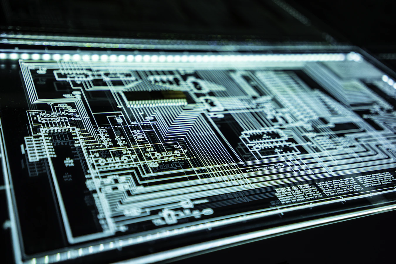
Mastering Light at the Nanoscale
How Coherent Control is Revolutionizing Plasmonic Computing
Imagine an internet that's not just faster, but instantaneous, with data processing happening at the speed of light in chips no thicker than a strand of DNA. This isn't science fiction—it's the promise of plasmonics.
Explore the TechnologyThe Promise of Plasmonic Computing
Recent breakthroughs in coherent control are turning the promise of plasmonics into reality, enabling ultra-fast, energy-efficient computing paradigms that could redefine modern technology.
Ultra-Fast Processing
Data processing at the speed of light with potentially terahertz operational speeds.
Energy Efficient
Up to 50% reduction in power consumption compared to previous systems.
Nanoscale Integration
67% reduction in circuit footprint enabling extreme miniaturization.
What Are Plasmon Resonances and Why Do They Matter?
The Nature of Plasmons
At the heart of this revolution are surface plasmon polaritons (SPPs)—special waves that are part light, part electron oscillation. These unique hybrid waves propagate along the interface between metals and dielectrics, confining light to incredibly small spaces at the nanoscale level1 .
1902
American physicist Robert Wood first noticed unusual optical effects on metallic gratings1 .
1960s
Development of practical excitation methods by Kretschmann, Raether, and Otto using prismatic structures1 .
Present
Advanced coherent control techniques enabling single-beam plasmonic logic circuits.
The Challenge of Traditional Control
Conventional plasmon control has faced significant limitations. Until recently, exciting SPPs required additional components like prisms or gratings to provide the necessary momentum match between light and plasmons1 .
This approach created bulky systems incompatible with modern miniaturization trends. Additionally, most plasmonic logic gates relied on interferometric structures or required secondary control lasers, complicating large-scale integration7 .
The Game-Changer: Coherent Control
Principles of Coherent Control
Coherent control represents a paradigm shift in how we manipulate plasmons. Instead of relying on physical structures or multiple beams, this approach uses the inherent wave properties of light itself—specifically, polarization and phase—to direct plasmonic behavior at the nanoscale.
The breakthrough lies in recognizing that different polarization states can be mapped to specific plasmonic responses. By carefully designing nanostructures that respond predictably to these polarization states, researchers can encode complex instructions into a single beam of light7 .
Recent Experimental Breakthroughs
In a landmark demonstration, researchers developed a single-beam logic framework using plasmonic two-wire transmission lines. This system utilizes six deterministic polarization states—four linear and two circular—to perform advanced computational operations without secondary control beams7 .
Polarization Modal Selectivity
Different polarization states excite distinct plasmonic modes for precise control.
Geometric Tuning
Nanostructures are designed to respond specifically to polarization inputs.
Single-Global Thresholding
A unified threshold mechanism converts analog plasmonic responses into digital logic states.
Minimal Circuit Footprint
67% reduction in size compared to previous systems7 .
Inside a Groundbreaking Experiment: Single-Beam Plasmonic Logic
Methodology and Setup
The experimental implementation of single-beam plasmonic logic represents a marvel of nanoscale engineering. Researchers fabricated specialized two-wire transmission lines (TWTLs) with integrated dimer and link input antennas. These structures serve as the interface where light is converted into controlled plasmonic signals7 .
Structure Fabrication
Creation of plasmonic two-wire transmission lines with precisely designed input antennas7 .
Polarization Encoding
Programming of six specific polarization states into a single laser beam7 .
Signal Processing
Plasmonic signals combine coherently at the output port7 .
Threshold Detection
Application of a single global threshold to convert analog interference to digital states7 .
Results and Significance
The experimental outcomes demonstrated remarkable capabilities for plasmonic computing:
| Metric | Performance | Improvement Over Previous Systems |
|---|---|---|
| Circuit Footprint | Minimal (nanoscale) | 67% reduction7 |
| Power Consumption | Ultra-low | 50% reduction7 |
| Control Complexity | Single beam, no auxiliary signals | Eliminates secondary lasers7 |
| Operational Speed | Ultrafast (potentially terahertz) | Limited only by plasmon decay times |
| Functionality Demonstrated | 2-bit comparator, parity checkers, encoder/decoder | Advanced logic operations |
Perhaps most significantly, the system solved a fundamental paradox in optical logic: how to generate a logical "1" output when both inputs are "0" without external energy sources. The single-global threshold mechanism combined with precise geometric control naturally enabled this critical (0,0→1) transition7 .
| Input Polarization | Branch A State | Branch B State | Output State | Logic Operation |
|---|---|---|---|---|
| 0° (on dimer) | 0 | 0 | 1 | NOT-type function |
| 90° (on dimer) | 1 | 1 | 0 | NOR-type function |
| ±45° (on dimer) | 1 or 0 | 0 or 1 | 0 | Routing function |
| LHCP/RHCP (on dimer) | Dominant/weak | Weak/dominant | 1 | OR-type function |
The Scientist's Toolkit: Essential Resources for Plasmonic Research
| Tool/Material | Function in Research | Example Applications |
|---|---|---|
| Gold & Silver Nanoparticles | Primary plasmonic materials | Fundamental studies, biosensing4 |
| Indium Tin Oxide (ITO) | Epsilon-near-zero material | Nonlinear optical switching9 |
| Quantum Dots | Gain medium for loss reduction | Coupler-free SPP excitation1 |
| Shadow Growth Technique | Nanofabrication method | Creating 3D hybrid nanostructures8 |
| Kretschmann-Raether Configuration | Plasmon excitation method | Prism-based coupling studies9 |
| Vanadyl Oxalate (VOC₂O₄) | Thermo-responsive material | Solid-state tunable nanoantennas6 |
| Two-Wire Transmission Lines | Plasmon waveguiding | Logic circuits, signal processing7 |
Beyond Computing: The Expanding Universe of Applications
The implications of coherent plasmon control extend far beyond computing:
Enhanced Security
Clock-inspired nanostructures with programmable polarization responses enable advanced anti-counterfeiting technologies. These "plasmonic rotamers" can store significant information and be used for secure verification of banknotes and important documents8 .
Ultra-Fast Optical Switching
Researchers have demonstrated all-optical switching in indium tin oxide (ITO) near its epsilon-near-zero point. This approach enables reflection changes from 1% to 45% with pump intensities of 70 GW cm⁻², potentially revolutionizing optical telecommunications9 .
Advanced Sensing
Plasmonic structures dramatically enhance sensitivity in biochemical detection. Surface-enhanced Raman spectroscopy (SERS) leverages plasmonic enhancement to detect single molecules, with applications ranging from medical diagnostics to environmental monitoring5 .

The Future of Plasmonic Control
As research progresses, several exciting directions are emerging:
Solid-State Tunable Systems
The development of thermo-responsive vanadyl oxalate nanoantennas addresses compatibility issues with traditional optoelectronics6 . These systems achieve reversible plasmon resonance shifts of up to 60 nm with switching speeds of hundreds of kilohertz.
Two-Dimensional Noble Metals
The exploration of materials like silverene and goldene promises new opportunities for electronic structure design and tuning of plasmon frequencies4 . These materials could lead to even more compact and efficient plasmonic devices.
Machine Learning Integration
The integration of machine learning concepts with plasmonic networks presents another fascinating frontier. The collective dynamics of adaptive memristor synapse-cascaded neural networks based on energy flow suggest potential for neuromorphic computing applications1 .
Commercial Applications
As these technologies mature, we stand at the threshold of a new computing paradigm: compact, energy-efficient, and ultrafast systems that process information at the speed of light. The age of plasmonic computing is dawning, and it promises to transform everything from personal devices to global telecommunications infrastructure.
A Bright Plasmonic Future
The coherent control of plasmon resonances represents more than just a technical achievement—it marks a fundamental shift in how we approach information processing at the nanoscale. By harnessing the unique properties of light-matter interactions, researchers are overcoming the limitations of conventional electronics and photonics.
The journey from Robert Wood's initial observations in 1902 to today's sophisticated coherent control strategies demonstrates how fundamental research, given time and persistence, can blossom into revolutionary technologies that reshape our world1 .