Nanoparticle Assembly Verification: A Correlative GISAXS and SEM Guide for Biomedical Research
This comprehensive guide explores the synergistic application of Grazing-Incidence Small-Angle X-ray Scattering (GISAXS) and Scanning Electron Microscopy (SEM) for verifying nanoparticle assemblies.
Nanoparticle Assembly Verification: A Correlative GISAXS and SEM Guide for Biomedical Research
Abstract
This comprehensive guide explores the synergistic application of Grazing-Incidence Small-Angle X-ray Scattering (GISAXS) and Scanning Electron Microscopy (SEM) for verifying nanoparticle assemblies. Targeted at researchers and drug development professionals, it provides foundational knowledge of both techniques, detailed protocols for their combined use, troubleshooting for common artifacts, and a comparative analysis of their strengths in quantifying order, spacing, and morphology. The article concludes with insights on how this correlative approach accelerates the development of reliable nanocarriers and functional nanostructured surfaces for advanced biomedical applications.
Understanding the Tools: GISAXS and SEM Fundamentals for Nano-Assembly Analysis
The Need for Multi-Scale Verification in Nanoparticle Assembly
The validation of nanoparticle superlattices and assemblies requires interrogation across length scales. Reliance on a single characterization technique can lead to incomplete or misleading structural interpretations. This guide compares the complementary roles of Grazing-Incidence Small-Angle X-ray Scattering (GISAXS) and Scanning Electron Microscopy (SEM) within a multi-scale verification framework, essential for applications like targeted drug delivery where structure dictates function.
Comparison Guide: GISAXS vs. SEM for Assembly Verification
Table 1: Direct Performance Comparison of Core Techniques
| Metric | GISAXS (X-ray Scattering) | Top-Down SEM (Imaging) | Cross-Sectional SEM/FIB-SEM |
|---|---|---|---|
| Primary Information | Statistical nanoscale order: lattice symmetry, unit cell size, crystal domain size. | Top-down mesoscale morphology: grain boundaries, large-area coverage, defects. | Vertical layer structure: film thickness, subsurface order, interface quality. |
| Field of View | ~mm² (beam footprint) | ~μm² to ~mm² (user-selectable) | ~μm² (cross-section) |
| Statistical Relevance | High (averages over billions of particles) | Low to Medium (localized images) | Very Low (destructive, local) |
| Depth Sensitivity | Penetrates entire film; provides ensemble average through thickness. | Surface-only (top ~ few nm for conductive coatings). | Explicit cross-sectional visualization. |
| Sample Preparation | Minimal (often in-situ, in native state). | Required (conductive coating, may induce artifacts). | Extensive, destructive (FIB milling, Pt deposition). |
| Quantitative Data | Crystallographic parameters, orientation distribution. | Particle size (2D projection), local packing metrics. | Layer thickness, vertical alignment precision. |
| Key Limitation | Cannot visualize point defects or grain boundaries directly. | No subsurface information; 2D projection only. | Destructive; not representative of entire sample. |
Table 2: Synergistic Data from Combined Multi-Scale Analysis
| Verification Parameter | GISAXS Data Input | SEM Data Input | Combined, Verified Conclusion |
|---|---|---|---|
| Long-Range Order | Sharp Bragg peaks indicate crystalline order. | Large, continuous domains observed. | Confirmed high-quality superlattice. |
| Lattice Constant | Precise value from q-positions (e.g., 15.2 ± 0.3 nm). | Measured from FFT of image (e.g., 14.8 ± 1.5 nm). | Validated measurement (15.0 ± 0.5 nm). |
| Domain Size | Calculated from peak broadening (e.g., ~1 μm). | Directly measured from images (e.g., 0.5-2 μm domains). | Confirms polycrystalline nature with micron-sized grains. |
| Assembly Defects | May not affect average peak position. | Clearly shows point defects, dislocations, grain boundaries. | Identifies defect types missed by GISAXS. |
| Vertical Structure | Layer spacing from out-of-plane peaks. | Cross-sectional SEM shows actual layer count & stacking. | Confirms intended layered heterostructure was achieved. |
Experimental Protocols for Correlative GISAXS-SEM
Protocol 1: In-Situ GISAXS During Drying-Mediated Assembly
- Sample Preparation: Disperse functionalized nanoparticles (e.g., 10nm Au, PEG-coated) in a volatile solvent (e.g., toluene) onto a clean silicon substrate.
- GISAXS Setup: Mount sample in a humidity/temperature-controlled chamber at the synchrotron beamline. Align grazing incidence angle (~0.2°).
- Data Acquisition: Begin scattering collection simultaneously with solvent drying. Use a fast 2D detector to collect frames (0.5-5s exposure) throughout the entire self-assembly process.
- Data Analysis: Integrate 2D patterns to 1D line cuts. Track the evolution of primary Bragg peak position (q*), intensity, and width to quantify the kinetics of lattice formation and domain growth.
Protocol 2: Ex-Situ Correlative GISAXS and SEM on the Same Spot
- Sample Marking: Use a focused ion beam (FIB) or laser marker to create a unique, findable coordinate system (fiducial marks) on the substrate around the assembly area.
- GISAXS Measurement: Map the sample using the fiducials, collecting GISAXS patterns at predefined points of interest (grid pattern). Record the motor positions for each point.
- Sample Transfer & Preparation: Carefully transfer the sample to a SEM. If non-conductive, apply a thin, uniform coating of Ir or Pt using a sputter coater (<5 nm).
- Correlative SEM Imaging: Navigate to the same motor coordinates using the fiducial marks. Acquire high-resolution top-down SEM images at the exact locations measured by GISAXS.
- Cross-Sectional Validation (Optional): For selected spots, use FIB to mill a cross-section perpendicular to the substrate. Deposit a protective Pt layer prior to milling. Image the cross-section to obtain vertical structure.
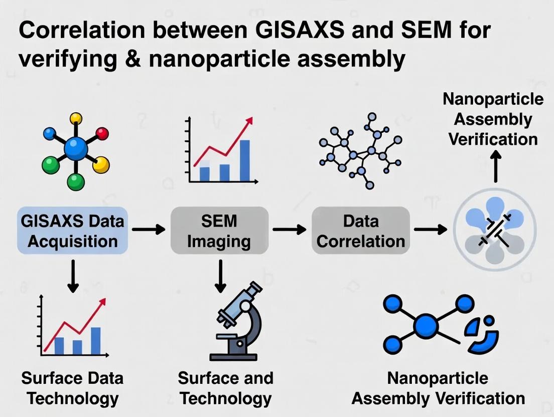
Visualization of the Multi-Scale Verification Workflow
Multi-Scale Verification Workflow
The Scientist's Toolkit: Research Reagent Solutions for Assembly & Analysis
Table 3: Essential Materials for Nanoparticle Assembly & Verification
| Item | Function & Importance |
|---|---|
| Functionalized Nanoparticles (e.g., Au, Fe3O4, PS with PEG, COOH, NH2 ligands) | Core building blocks. Surface chemistry dictates interaction potential and self-assembly pathway. |
| Ultra-Flat Substrates (Silicon wafers, Mica, ITO-coated glass) | Provide a smooth, uniform surface for homogeneous nucleation and growth of assemblies. Critical for GISAXS. |
| Precision Syringe Pumps & Teflon Wells | Enable controlled, slow solvent evaporation—the key to achieving large-domain ordered films. |
| Conductive Coatings (Iridium, Platinum, Carbon) | Applied as thin (~3-5 nm) films via sputter coating for SEM imaging of non-conductive samples without charging artifacts. |
| FIB Lift-Out Kit (Pt Gas Injector, Micromanipulator) | For site-specific cross-section preparation. Allows precise targeting of GISAXS-measured areas for vertical validation. |
| Calibrated Grating & NIST Standards (e.g., Si powder, Ag behenate) | For accurate calibration of the GISAXS/SANS detector q-range and spatial distortion, ensuring precise d-spacing calculation. |
| GISAXS Analysis Software (e.g., GIXSGUI, IsGISAXS, SASfit) | Used to model 2D scattering patterns, fit peak positions, and extract quantitative structural parameters from raw data. |
| Correlative Microscopy Software (e.g., MAPS, Linkam) | Aligns and overlays GISAXS spatial maps with SEM/optical images, enabling true position-specific correlation. |
Grazing-Incidence Small-Angle X-ray Scattering (GISAXS) is a critical, non-destructive technique for the statistical characterization of nanoscale order in thin films over large areas. This guide compares its performance with primary alternative techniques within the context of verifying nanoparticle assembly, specifically correlating with Scanning Electron Microscopy (SEM) data.
Performance Comparison: GISAXS vs. Alternative Characterization Techniques
Table 1: Comparison of Techniques for Nanoparticle Assembly Analysis
| Technique | Spatial Resolution | Probing Depth & Area | Statistical Relevance | Sample Environment | Key Measurable Parameters |
|---|---|---|---|---|---|
| GISAXS | ~1-100 nm (lateral), Ångström (vertical) | Whole film thickness; mm² to cm² area | Excellent (billions of nanoparticles) | Ambient, in situ liquid/gas possible | Size, shape, spacing, order, film thickness, roughness. |
| Scanning Electron Microscopy (SEM) | <1 nm to few nm | Surface/edge; µm² to mm² area | Poor (manual counting of 100s-1000s) | High vacuum typically | Direct imaging of local morphology, size, spacing. |
| Atomic Force Microscopy (AFM) | ~1 nm lateral, <0.1 nm vertical | Surface only; µm² to ~100 µm² area | Moderate (1000s of nanoparticles) | Ambient, liquid possible | 3D surface topography, size, local order. |
| Transmission Electron Microscopy (TEM) | <0.2 nm | Local thin section; µm² area | Very Poor (manual analysis of 10s-100s) | High vacuum | Atomic-scale structure, crystallinity, precise size/shape. |
Experimental Protocols for GISAXS-SEM Correlation
Protocol 1: GISAXS Measurement of Nanoparticle Thin Films
- Sample Alignment: Mount the thin-film sample on a high-precision goniometer. Use a laser guide to align the sample surface co-planar with the incident X-ray beam (grazing angle α~i~).
- Angle Optimization: Perform an incident angle (α~i~) scan through the critical angle of the film/substrate to maximize scattering intensity and minimize background. Typical α~i~ ranges from 0.1° to 0.5°.
- Data Acquisition: Illuminate the sample with a collimated, monochromatic X-ray beam (e.g., Cu Kα, λ = 1.54 Å). Use a 2D area detector (e.g., Pilatus) placed several meters downstream to capture the scattering pattern. Exposure times range from 1-300 seconds.
- Data Reduction: Apply geometric corrections, subtract background scattering, and perform sector cuts or full pattern fitting to extract quantitative parameters (e.g., inter-particle distance from Bragg rod positions, particle size from form factor oscillations).
Protocol 2: Correlative SEM Validation of GISAXS Data
- Sample Marking: Use a focused ion beam (FIB) or mechanical scribe to create fiduciary markers near the region measured by GISAXS for precise relocation.
- SEM Imaging: Image multiple (e.g., 10-20) regions across the GISAXS-illuminated area at high magnification (e.g., 100kX). Use consistent imaging parameters (voltage, working distance).
- Image Analysis: Use automated particle analysis software (e.g., ImageJ, Gwyddion) to extract nanoparticle center positions, diameters, and nearest-neighbor distances from thresholded SEM images.
- Statistical Correlation: Compare the probability distribution functions (PDFs) of particle spacing from SEM image analysis with the PDF derived from the GISAXS data via pair distance distribution function (PDDF) analysis. A strong correlation validates the GISAXS model.
Visualization of the GISAXS-SEM Correlation Workflow
Title: GISAXS-SEM Correlation Workflow for Assembly Verification
The Scientist's Toolkit: Key Research Reagent Solutions
Table 2: Essential Materials for GISAXS/SEM Nanoparticle Studies
| Item | Function |
|---|---|
| Monodisperse Nanoparticle Suspension (e.g., Au, SiO₂ in toluene/water) | Provides the fundamental building blocks with controlled size and shape for assembly. |
| Functionalized Substrate (e.g., Si wafer with self-assembled monolayer) | Presents a tailored surface for controlled nanoparticle deposition via chemical interaction. |
| Precision Spin Coater | Enables the creation of uniform thin films via controlled solvent evaporation and deposition. |
| Synchrotron Beamtime / Lab-Source X-ray Instrument | Produces the high-flux, collimated X-ray beam required for GISAXS measurements. |
| 2D X-ray Area Detector (e.g., Pilatus, Eiger) | Captures the faint scattering pattern with high sensitivity and low noise. |
| GISAXS Analysis Software (e.g., GIXSGUI, IsGISAXS, FitGISAXS) | Enables modeling and quantitative extraction of nanoscale parameters from complex 2D data. |
| Field-Emission SEM (FE-SEM) | Provides high-resolution, high-magnification imaging of nanoparticle arrangements. |
| Image Analysis Suite (e.g., ImageJ/Fiji, Gwyddion) | Facilitates automated, statistical analysis of particle size and spacing from SEM images. |
Within a broader thesis on the correlation of Grazing-Incidence Small-Angle X-Ray Scattering (GISAXS) with Scanning Electron Microscopy (SEM) for nanoparticle assembly verification, SEM serves as the critical, high-resolution counterpart to the statistical, ensemble-averaged data from GISAXS. This guide compares the performance of modern SEM instruments in visualizing local morphology and defects, a capability essential for researchers and drug development professionals validating nanoscale drug delivery systems and assemblies.
Performance Comparison: High-Resolution SEM Systems
The following table compares key performance metrics of three prevalent SEM types used in nanomaterials research, based on current manufacturer specifications and published literature.
Table 1: Comparison of SEM System Performance for Nanomaterial Imaging
| Feature / Model | Conventional Thermal Emission SEM (e.g., JEOL JSM-IT500) | Schottky Field Emission SEM (FESEM) (e.g., Zeiss Gemini) | Cold Cathode FESEM (e.g., Hitachi Regulus) | Primary Use Case in GISAXS Correlation |
|---|---|---|---|---|
| Typical Resolution | 3.0 nm @ 30 kV | 0.6 nm @ 15 kV | 0.8 nm @ 15 kV | Defining upper limit of detectable feature size. |
| Accelerating Voltage Range | 0.3 to 30 kV | 0.02 to 30 kV | 0.5 to 30 kV | Low-V for surface, high-V for subsurface defects. |
| Beam Current Stability | High | Very High | Moderate | Critical for consistent, quantitative image analysis. |
| Sample Chamber Size | Large (~Ø 200 mm) | Medium | Medium | Limits sample holder compatibility for in-situ cells. |
| Low-Vacuum Mode | Standard | Optional (VP mode) | Standard | Essential for non-conductive, uncoated biomaterials. |
| Typical Cost Bracket | $$ | $$$ | $$$$ | Access vs. capability trade-off. |
Experimental Protocols for Correlative GISAXS-SEM Analysis
Protocol 1: Direct Correlation on a Identical Sample Region
Objective: To directly link GISAXS statistical data with localized SEM morphology.
- Sample Preparation: Spin-coat nanoparticle suspension on a marked, conductive silicon substrate (e.g., with lithographic coordinates).
- GISAXS Measurement: Perform GISAXS scan at synchrotron beamline. Record beam footprint location relative to substrate markers.
- Sample Transfer & Coating: If non-conductive, apply a sub-2 nm conductive coating (Iridium or Platinum) via high-resolution sputter coater.
- SEM Imaging: Relocate the exact GISAXS footprint using substrate markers. Acquire high-resolution (≤ 1 nm) SEM images at multiple magnifications across the footprint area under low kV (1-5 kV) to minimize penetration and highlight surface morphology.
- Data Correlation: Compare SEM-observed packing density, defect types (cracks, vacancies), and local order with the peak positions, shapes, and intensities in the GISAXS pattern.
Protocol 2: Comparative Analysis of Defect Populations
Objective: To quantify defect types influencing GISAXS diffuse scattering.
- Sample Set: Prepare a series of nanoparticle films with controlled variation (e.g., drying rate, ligand density).
- Ensemble Characterization: Acquire GISAXS patterns for each sample to measure coherence length and diffuse scattering halo intensity.
- Localized SEM Sampling: For each sample, acquire at least 10 high-resolution SEM images from random, non-adjacent locations.
- Image Analysis: Use thresholding and particle analysis software (e.g., ImageJ, Fiji) to quantify:
- Areal defect density (voids per µm²).
- Average domain size of ordered regions.
- Classification of defect types (point vacancies, line defects, grain boundaries).
- Correlation: Plot quantified SEM defect density against GISAXS-derived paracrystalline distortion parameters or diffuse scattering intensity.
Diagram: Correlative GISAXS-SEM Workflow for Nanoparticle Assembly
Title: Workflow for GISAXS-SEM Correlation in Nanoparticle Analysis
The Scientist's Toolkit: Essential Research Reagent Solutions
Table 2: Key Materials for SEM Sample Preparation in Nanoparticle Studies
| Item | Function & Rationale |
|---|---|
| Conductive Silicon Wafers with Markers | Preferred substrate. Provides flat, conductive surface and fiducial marks for relocating GISAXS footprint. |
| High-Resolution Sputter Coater (Iridium/Pt) | Applies ultra-thin (1-2 nm), fine-grained conductive layer to non-conductive samples, preserving nanoscale surface details. |
| Conductive Carbon Tape / Silver Paste | Provides electrical and mechanical contact between sample and stub, preventing charging artifacts. |
| Plasma Cleaner (O₂/Ar) | Cleans substrate surfaces to ensure uniform nanoparticle wetting and removes organic contaminants prior to imaging. |
| Critical Point Dryer | Preserves delicate, solution-phase nanoparticle aggregates or soft-matter assemblies by replacing solvent with CO₂, avoiding collapse. |
| Reference Nanoparticle Standards (e.g., 100 nm Au) | Used for daily SEM magnification calibration and resolution verification, ensuring measurement accuracy. |
Within the context of nanoparticle assembly verification research, the characterization of nanoscale order, morphology, and defect structure is paramount. Grazing-Incidence Small-Angle X-ray Scattering (GISAXS) and Scanning Electron Microscopy (SEM) are frequently employed techniques. A common misconception is that they serve redundant purposes. This guide objectively compares their performance, demonstrating that their integration provides a comprehensive, multiscale verification strategy essential for robust research in fields like drug delivery system development.
Core Principle Comparison
Table 1: Fundamental Comparison of GISAXS and SEM
| Feature | GISAXS (Grazing-Incidence Small-Angle X-Ray Scattering) | SEM (Scanning Electron Microscopy) |
|---|---|---|
| Primary Probe | X-ray photons (coherent) | Electron beam |
| Information Type | Statistical, ensemble-averaged structural data | Direct, real-space imaging |
| Field of View | Macroscopic (mm² area, µm depth) | Localized (µm² to mm² surface) |
| Sample Penetration | Yes (bulk-sensitive, probes film interior) | No (primarily surface-sensitive, ~nm-µm depth) |
| Primary Output | Reciprocal-space scattering pattern (q-space) | Real-space micrograph (x,y-space) |
| Key Measurables | Nanoscale periodicity, particle size/distribution, lattice symmetry, pore correlation | Surface topography, individual particle shape/morphology, local defects, direct spatial arrangement |
| Statistical Relevance | High (averages over billions of nanoparticles) | Lower (represents a specific, localized region) |
| Sample Preparation | Minimal (often requires flat substrate) | Can be extensive (conductive coating, cross-sectioning) |
| In-situ Capability | Excellent (for kinetics, environmental cells) | Limited (requires high vacuum, specialized stages) |
Experimental Data & Performance Comparison
Table 2: Complementary Data from a Model Nanoparticle Array Study
| Analysis Goal | GISAXS Data | SEM Data | Synergistic Interpretation |
|---|---|---|---|
| Average Center-to-Center Distance | Primary Bragg peak at q_y = 0.0125 Å⁻¹ | Manual measurement of 50 particles in image. | GISAXS: D = 2π/q_y = 50.2 nm (ensemble avg). SEM: 49.8 ± 3.1 nm (local avg). Correlation confirms long-range order. |
| Particle Size / Shape | Form factor oscillations modelled as spheres of radius R. | Direct visualization shows quasi-spherical shapes. | GISAXS: R = 14.5 nm. SEM: Average diameter = 29.3 nm. GISAXS probes core, SEM includes surface coating/contrast. |
| Lattice Type & Disorder | Distinct Bragg rod pattern indicates hexagonal symmetry. Paracrystal model fits disorder (σ/D ~ 8%). | Image shows hexagonal domains separated by defect lines (grain boundaries). | GISAXS quantifies degree of disorder statistically. SEM identifies the nature and location of defects (e.g., dislocations, vacancies). |
| Film Thickness / Layering | Yoneda wing and thickness fringes indicate film thickness of 102 nm. | Cross-sectional SEM confirms a bilayer structure, total thickness ~105 nm. | GISAXS non-destructively measures total film thickness and internal density profile. SEM visually confirms layering and interface sharpness. |
Detailed Experimental Protocols
Protocol 1: GISAXS for Nanoparticle Superlattice Characterization
- Sample Preparation: Spin-coat nanoparticle suspension (e.g., 20 mg/mL Au NPs in toluene) onto a clean silicon wafer. Anneal at 80°C for 1 hour to promote self-assembly.
- Instrument Setup: At a synchrotron beamline, align the sample at a grazing incidence angle (αi ≈ 0.2°, above the critical angle of the film/substrate).
- Data Collection: Use a 2D pixelated detector (e.g., Pilatus 2M) placed ~3-5 m from the sample. Collect scattering pattern with exposure times of 1-10 seconds.
- Data Reduction: Correct for detector geometry, beam stop shadow, and background scattering.
- Data Analysis: Integrate the 2D pattern along the qz (out-of-plane) direction to analyze in-plane (qy) structure. Model with Distorted Wave Born Approximation (DWBA) and paracrystal models to extract parameters (lattice spacing, disorder parameter, particle size).
Protocol 2: SEM for Correlative Local Verification
- Sample Preparation: Apply a thin (~5 nm) conductive coating (e.g., Iridium) via sputter coater to mitigate charging, as the nanoparticle film is often non-conductive.
- Instrument Setup: Use a field-emission SEM (e.g., Zeiss Gemini). Operate at low accelerating voltage (3-5 kV) to enhance surface detail and minimize sample damage.
- Imaging: Locate the general area measured by GISAXS (if not the exact spot). Acquire micrographs at multiple magnifications (e.g., 50kX for lattice order, 200kX for individual particles).
- Image Analysis: Use software (e.g., ImageJ, Fiji) for Fast Fourier Transform (FFT) to assess periodicity and manual/automated particle analysis to determine local size distribution and defect density.
Visualizing the Synergistic Workflow
(Diagram Title: Synergistic Workflow for Assembly Verification)
(Diagram Title: Probe & Information Depth Comparison)
The Scientist's Toolkit: Key Research Reagent Solutions
Table 3: Essential Materials for Nanoparticle Assembly Verification
| Item | Function in Research | Example/Note |
|---|---|---|
| Functionalized Nanoparticles | Core building blocks for self-assembly. | Au NPs with PEG-thiol ligands for biocompatibility; polystyrene NPs for model systems. |
| Flat, Low-Roughness Substrates | Provide a defined interface for ordered assembly. | Silicon wafers (P-type, <100>), glass coverslips, or mica sheets. |
| Precision Spin Coater | Creates uniform thin films of nanoparticle solutions. | Parameters (rpm, acceleration, time) control film thickness and order. |
| Conductive Sputter Coater | Applies ultra-thin conductive metal layer for SEM. | Iridium or gold-palladium targets preferred for high-resolution, low-charging coatings. |
| Calibration Standards | Essential for both GISAXS and SEM instrument calibration. | GISAXS: Silver behenate powder (d-spacing = 58.38 Å). SEM: Grating with known pitch (e.g., 1000 lines/mm). |
| Image Analysis Software | Quantifies particle size, spacing, and order from SEM micrographs. | Fiji/ImageJ with specialized plugins (e.g., "ParticleSizer", "Gwyddion"). |
| Scattering Analysis Suite | Models and extracts quantitative parameters from GISAXS patterns. | Irena (Igor Pro) or BornAgain (open-source) software packages. |
Thesis Context: GISAXS-SEM Correlation for Nanoparticle Assembly Verification
This comparison guide is situated within a broader research thesis investigating the correlative use of Grazing-Incidence Small-Angle X-ray Scattering (GISAXS) and Scanning Electron Microscopy (SEM) for the quantitative verification of self-assembled nanoparticle monolayers. The synergy of these techniques provides a statistically robust, multi-scale analysis of nanostructured surfaces, which is critical for applications in catalysis, photonics, and targeted drug delivery systems where surface functionalization with nanoparticles is key.
Performance Comparison of Characterization Techniques
The following table compares the capabilities of primary techniques for analyzing nanoparticle assemblies, based on current experimental literature.
Table 1: Comparison of Techniques for Nanoparticle Assembly Characterization
| Parameter | GISAXS | SEM | Atomic Force Microscopy (AFM) | Dynamic Light Scattering (DLS) |
|---|---|---|---|---|
| Primary Measured | Ensemble-averaged order, spacing, domain size, morphology (form factor). | Direct imaging of local order, spacing, individual particle morphology. | Topography and height profiles; local mechanical properties. | Hydrodynamic size distribution in solution (pre-deposition). |
| Lateral Order | Quantitative via Bragg rod analysis; excellent for hexagonal/ cubic order. | Qualitative/visual; can quantify via image analysis over small areas. | Limited to scanned area; tip convolution can affect accuracy. | Not applicable (solution phase). |
| Mean Spacing | High precision from peak positions in scattering pattern. | Direct measurement from images; statistical sampling required. | Direct measurement; limited field of view. | Not applicable. |
| Domain Size | Calculated from Scherrer analysis of peak broadening; ensemble average. | Visually identifiable; manual or algorithmic domain mapping. | Challenging to define over large scans. | Not applicable. |
| Particle Morphology | Inferred from form factor fitting (sphere, cylinder, etc.). | Direct visualization; high-resolution shape determination. | 3D topography; shape information can be obscured by tip geometry. | Assumes spherical model; provides size distribution only. |
| Throughput & Statistics | Excellent; probes mm² area, billions of particles. | Slower; statistics depend on number of images analyzed. | Very slow; limited field of view. | Fast; high ensemble statistics in solution. |
| Sample Environment | Ambient, vacuum, or in-liquid cells possible. | High vacuum typically required (can use low-vac for non-conductive). | Ambient, liquid, or controlled environments. | Solution phase only. |
| Key Limitation | Indirect imaging; requires modeling; limited to periodic structures. | Sample must be conductive; electron beam may damage soft materials. | Slow scan speed; potential sample deformation; small analyzed area. | Only for particles in suspension; assumes spherical morphology. |
Experimental Protocols for Correlative GISAXS-SEM Analysis
Protocol 1: Sample Preparation for Nanoparticle Monolayer Assembly
- Materials: Silicon wafer (or other flat substrate), functionalized nanoparticles in colloidal suspension (e.g., polystyrene, gold, or silica), piranha solution (3:1 H₂SO₄:H₂O₂), Langmuir-Blodgett trough or drop-casting setup, spin coater.
- Procedure:
- Clean substrate in piranha solution for 30 minutes, rinse with deionized water, and dry under nitrogen stream. (CAUTION: Piranha is extremely corrosive and exothermic.)
- Functionalize nanoparticles per synthesis protocol to ensure monodispersity and surface charge stability.
- For Langmuir-Blodgett: Spread nanoparticle suspension on the air-water interface of the trough. Compress the barrier slowly to achieve the desired surface pressure. Dipping the substrate vertically transfers the monolayer.
- For Drop-Casting/Spin-Coating: Deposit a controlled volume of nanoparticle suspension onto the substrate. For spin-coating, immediately accelerate to a predefined speed (e.g., 2000-5000 rpm for 30-60s) to spread and evaporate solvent rapidly.
- Anneal the sample if required (e.g., 2 hours at 80°C for polymer nanoparticles) to improve adhesion and order.
Protocol 2: GISAXS Measurement and Data Reduction
- Instrumentation: Synchrotron beamline or laboratory-scale GISAXS setup with a micro-focus X-ray source, 2D detector.
- Procedure:
- Align the sample at a grazing incidence angle (αᵢ) typically between 0.1° and 0.5°, just above the critical angle of the substrate to enhance surface sensitivity.
- Acquire 2D scattering pattern with exposure times from seconds (synchrotron) to hours (lab source).
- Use software (e.g., GIXSGUI, FitGISAXS, BornAgain) for data reduction: correct for detector flat field, beam stop shadow, and incident angle.
- Perform an azimuthal integration of the scattering pattern to generate 1D intensity profiles along the in-plane (qᵧ) and out-of-plane (q₂) directions.
- Analyze in-plane peaks: The primary peak position (q) gives the mean center-to-center distance (d = 2π/q). The peak full-width at half-maximum (FWHM, Δq) yields the correlation length (domain size, ξ ≈ 2π/Δq) via Scherrer analysis.
Protocol 3: Correlative SEM Imaging and Analysis
- Instrumentation: Field-Emission Scanning Electron Microscope (FE-SEM).
- Procedure:
- Mount the GISAXS-measured sample on an SEM stub. Apply a thin conductive coating (e.g., 5 nm Ir or Au-Pd) if the nanoparticles are non-conductive.
- Image the sample at low magnification (e.g., 5kX) to locate the general area probed by the X-ray beam (often marked by a laser or visible marker).
- Acquire high-resolution images (e.g., 50kX - 100kX) from multiple, random locations within the irradiated area to ensure statistical relevance.
- Use image analysis software (e.g., ImageJ, Fiji, or commercial packages) to:
- Apply a threshold to binarize the image.
- Perform particle identification and centroid calculation.
- Calculate a 2D Fast Fourier Transform (FFT) to assess periodicity.
- Determine the nearest-neighbor distances and radial distribution function (RDF) to quantify local order and spacing.
Visualization of the Correlative Workflow
Diagram Title: GISAXS-SEM Correlative Analysis Workflow
The Scientist's Toolkit: Key Research Reagent Solutions
Table 2: Essential Materials for Nanoparticle Assembly & Characterization
| Item | Function / Role in Research |
|---|---|
| Functionalized Nanoparticles | Core building blocks (e.g., amine- or carboxyl-terminated polystyrene, PEGylated gold nanospheres). Surface chemistry dictates assembly behavior and biomolecular conjugation. |
| Ultra-Flat Substrates | Silicon wafers, glass coverslips, or mica. Provide an atomically smooth surface to minimize substrate-induced disorder during assembly. |
| Piranha Solution | A mixture of concentrated sulfuric acid and hydrogen peroxide. Extremely powerful oxidizing agent for removing organic residues and hydroxylating substrate surfaces. |
| Langmuir-Blodgett Trough | Precision instrument to compress nanoparticle monolayers at the air-liquid interface for transfer onto solid substrates with high uniformity. |
| Spin Coater | Provides rapid, reproducible deposition of nanoparticle films by spreading suspension via centrifugal force and controlled evaporation. |
| Conductive Coating Materials | Iridium or gold-palladium sputtering targets. Applied as a thin layer on non-conductive samples to prevent charging during SEM imaging. |
| GISAXS Analysis Software (e.g., GIXSGUI, BornAgain). Enables modeling and fitting of 2D scattering patterns to extract quantitative structural parameters. | |
| Image Analysis Suite (e.g., Fiji/ImageJ with plugins). Used for automated particle detection, FFT analysis, and statistical measurement from SEM micrographs. |
Step-by-Step Protocol: Correlative GISAXS-SEM for Assembly Verification
Sample Preparation Strategies for Compatible GISAXS and SEM Measurement
This guide is framed within a thesis research context focusing on verifying nanoparticle self-assembly structures through the correlation of Grazing-Incidence Small-Angle X-ray Scattering (GISAXS) with Scanning Electron Microscopy (SEM). The objective is to compare sample preparation strategies that enable sequential, non-destructive, and compatible measurement using both techniques, which have inherently different operational environments and sample requirements.
Key Challenges in Compatible Sample Preparation
The primary challenge lies in reconciling the requirements of both techniques. GISAXS typically requires a flat, smooth substrate over a large area (several mm²) to obtain a statistically significant scattering signal from nanoparticle assemblies. SEM, especially high-resolution SEM, may require conductive coatings to prevent charging, which can alter or obscure the GISAXS signal. Furthermore, SEM sample handling can introduce contamination or damage that compromises subsequent GISAXS analysis.
Comparison of Sample Preparation Strategies
The following table summarizes and compares four principal strategies for compatible GISAXS/SEM sample preparation, based on current research methodologies.
Table 1: Comparison of Compatible GISAXS/SEM Sample Preparation Strategies
| Strategy | Core Methodology | GISAXS Compatibility | SEM Compatibility (Uncoated) | Risk of Sample Alteration | Best For Assembly Type |
|---|---|---|---|---|---|
| Conductive Substrates | Use of intrinsically conductive substrates (e.g., doped silicon, ITO-glass, HOPG). | High. Provides flat, smooth surface. | Moderate to High. Reduces charging. | Low. No coating applied. | Polymer & inorganic NPs on ITO; nanocrystals on HOPG. |
| Ultra-Thin Carbon Film | Spin-coating or floating a sub-5 nm amorphous carbon film onto a standard Si wafer. | High. Minimal scattering/absorption. | High. Provides conductivity and stability. | Moderate. May slightly dampen GISAXS features. | Delicate organic/biological templates; colloidal crystals. |
| GISAXS-first, Low-Vacuum SEM | Perform GISAXS on pristine samples, then use low-vacuum or environmental SEM without coating. | Optimal (pristine sample). | Low to Moderate. Imaging may be challenging for fine features. | Very Low for GISAXS; possible beam damage in SEM. | Charge-sensitive materials like block copolymer thin films. |
| Strategic Metallization | Apply an extremely thin (1-2 nm), discontinuous layer of Pt/Pd via low-angle sputtering after GISAXS. | Must be performed after GISAXS measurement. | High. Enables high-resolution imaging. | High for post-GISAXS analysis. Alteration is intentional. | Verifying GISAXS models of packed 3D superlattices. |
Experimental Protocols for Featured Strategies
Protocol A: Ultra-Thin Carbon Film on Silicon Wafer
- Substrate Cleaning: Piranha etch (3:1 H₂SO₄:H₂O₂) a standard <100> silicon wafer for 15 minutes. CAUTION: Extremely hazardous. Rinse thoroughly with deionized water and dry under N₂ stream.
- Carbon Deposition: Using a carbon coater, evaporate a high-purity carbon rod onto a freshly cleaved mica sheet to a thickness of ~4-5 nm.
- Film Transfer: Float the carbon film on a deionized water surface and submerge the cleaned Si wafer beneath it. Carefully lift the wafer to capture the film on its surface. Dry overnight in a desiccator.
- Nanoparticle Assembly: Deposit nanoparticle solution (e.g., 50 µL of 1 wt% polystyrene-gold core-shell in toluene) via spin-coating at 2000 rpm for 60 seconds.
- Measurement Sequence: Perform GISAXS measurement first. Subsequently, image the same sample location in SEM at 5-10 kV without any additional coating.
Protocol B: Strategic Post-GISAXS Metallization for 3D Superlattices
- Substrate Preparation: Use a polished, single-crystal silicon substrate with a native oxide layer.
- Assembly Formation: Assemble oleylamine-capped PbS nanocrystals into a superlattice via controlled solvent evaporation in a saturated toluene vapor environment.
- GISAXS Measurement: Collect a full GISAXS pattern at a synchrotron beamline, mapping the sample stage to identify regions of interest with high superlattice order.
- Targeted Metallization: In a sputter coater, deposit a nominal 1.5 nm layer of Pt/Pd (80/20) onto the sample at a low incident angle (15-20° from the sample plane). This creates a discontinuous, conformal layer that enhances conductivity while preserving topographic detail.
- High-Resolution SEM: Image the metallized region at 3-5 kV to directly visualize the nanocrystal packing and correlate with the GISAXS-derived lattice parameters.
Workflow Diagram for Correlative Analysis
Diagram Title: Workflow for Correlative GISAXS-SEM Analysis of NP Assemblies
The Scientist's Toolkit: Essential Research Reagent Solutions
Table 2: Key Materials for Compatible GISAXS/SEM Sample Preparation
| Item | Function in Compatible Prep | Example Product/ Specification |
|---|---|---|
| P-doped Silicon Wafers | Provides a flat, low-RMS roughness, and mildly conductive substrate. Reduces SEM charging. | 〈100〉, 0.001-0.005 Ω·cm resistivity, single-side polished. |
| Indium Tin Oxide (ITO) Glass | Optically transparent, conductive substrate for in-situ or ex-situ studies requiring transparency. | Sheet resistance < 15 Ω/sq, RMS roughness < 5 nm. |
| Highly Ordered Pyrolytic Graphite (HOPG) | Atomically flat, conductive surface ideal for imaging isolated nanoparticles or 2D arrays. | ZYA or ZYB grade, freshly cleaved before use. |
| Ultra-Thin Carbon Film on TEM Grid | Provides a conductive, electron-transparent support. Can be floated and transferred to a Si wafer. | 3-5 nm thick, 300 mesh copper grid with lacey carbon. |
| Low-Angle Sputter Coater | Applies ultra-thin, conformal conductive metal layers to minimize feature obscuration. | Equipped with Pt/Pd target, rotational/tilt stage. |
| Conductive Carbon Tape | For creating a secure, conductive path from the sample surface to the SEM stub. Must be placed outside GISAXS beam path. | Double-sided, high-purity carbon. |
| Spin Coater with Vacuum Chuck | For creating uniform nanoparticle films and uniform conductive polymer layers (e.g., PEDOT:PSS). | Programmable speed (100-6000 rpm), compatible with small substrates. |
Successful correlation between GISAXS and SEM data hinges on a sample preparation strategy that prioritizes the integrity of the nanostructure while mitigating the technical constraints of each instrument. For most research within the thesis context, the use of conductive substrates (Strategy 1) or ultra-thin carbon supports (Strategy 2) provides the best balance, allowing sequential measurement with minimal alteration. When ultimate SEM image quality is required for complex 3D assemblies, strategic post-GISAXS metallization (Strategy 4) is the recommended approach, accepting that the SEM sample is intentionally altered after the pristine GISAXS data is collected. The choice depends critically on the nature of the nanoparticle assembly and the specific structural parameters under investigation.
In research correlating Grazing-Incidence Small-Angle X-ray Scattering (GISAXS) with Scanning Electron Microscopy (SEM) for verifying nanoparticle assembly, the initial data acquisition step is critical. Proper beam alignment and parameter optimization directly determine the quality of the structural data used for later correlation. This guide compares the performance of different instrumental configurations and methodologies for this crucial step.
Comparative Performance Analysis
The following table summarizes key performance metrics for different GISAXS alignment strategies, based on recent experimental studies. The primary figure of merit is the achieved angular resolution (Δα_f) of the incident beam, which governs the precision in probing the in-plane and out-of-plane nanostructure.
Table 1: Comparison of GISAXS Beam Alignment & Optimization Methodologies
| Methodology / System | Key Principle | Achieved Angular Resolution (Δα_f) | Typical Alignment Time (min) | Required Sample Prep | Best For Assembly Type | Primary Limitation |
|---|---|---|---|---|---|---|
| Laser Alignment Kit (Standard) | Visual coarse alignment using coaxial laser. | ~0.05° | 15-20 | Standard substrate | Large domains (>1 µm), sparse arrays | Prone to user error; poor for grazing angles < 0.2°. |
| Direct Beam Diode Scan | Scanning a diode detector through direct beam to find maximum. | ~0.02° | 10-15 | Must withstand direct beam | Robust films, preliminary tests | Risk of sample damage; no real-time sample visualization. |
| Sample Surface Reflectivity Curve | Measuring specular reflectivity vs. incident angle to find critical angle (α_c). | ~0.005° | 25-35 | Flat, reflective substrate | Thin films, ordered lattices | Time-consuming; requires homogeneous surface. |
| Pilatus Detector Quick Exposure | Using 2D detector exposure to visualize footprint and Yoneda wing. | ~0.01° (visual) | 5-10 | Any | All, especially rough films | Qualitative; requires experience to interpret scattering pattern. |
| Automated Alignment (e.g., SAXSbot) | Motorized stages with feedback from ion chamber or diode. | ~0.01° | 2-5 (post-setup) | Standard substrate | High-throughput screening | High initial cost and setup complexity. |
Detailed Experimental Protocols
Protocol A: Sample Surface Reflectivity Curve for Precision Alignment
This is the gold-standard method for achieving the highest angular resolution, essential for correlating subtle nanostructural features with SEM.
- Setup: Place sample on goniometer. Use a point detector (e.g., scintillation counter) or the lowest pixel row of a 2D detector. Set a very narrow incident slit (e.g., 50 µm).
- Scan: Perform an ω (theta) scan over a range from 0° to typically 1.0° (or 2 * α_c) with a very small step size (e.g., 0.001°). Measure the intensity of the specularly reflected beam.
- Analysis: Plot intensity vs. incident angle (ω). Identify the critical angle (α_c) where intensity drops sharply. This feature is substrate-dependent.
- Optimization: Set the optimal GISAXS incident angle (αi). For probing near-surface structure, set αi slightly above αc (e.g., αc + 0.1°). For bulk film probing, set αi higher (e.g., αc + 0.5°).
- Verification: Take a short GISAXS exposure. A well-defined Yoneda band and clear Bragg rods/rings indicate successful alignment.
Protocol B: Pilatus Detector Quick Exposure for Rapid Assessment
Used for fast initial alignment and qualitative assessment of sample quality.
- Setup: Insert beamstop. Set incident angle to an estimated value (e.g., 0.2° for soft matter on silicon). Use medium slit settings (e.g., 200 µm).
- Exposure: Take a very short exposure (0.1-0.5 seconds).
- Interpretation:
- Beam Footprint: Check the vertical extension of the direct beam shadow. Adjust the sample height (Y) to minimize the footprint, centering it on the detector.
- Yoneda Band: Observe the curved, high-intensity region. Its maximum should be visible. Fine-tune α_i to position the Yoneda band optimally.
- Scattering Features: Look for streaks (indicating ordered structures) or rings (for isotropic assemblies).
Protocol C: Automated Alignment with Feedback Loop
Common in synchrotron beamlines and advanced lab systems.
- Calibration: Define scan ranges and safety limits for motors (sample X, Y, Z, tilt, goniometer ω).
- Programming: Script a routine that:
- Scans ω while monitoring ion chamber current.
- Finds the maximum current (direct beam transmission) or the steepest drop (reflectivity edge).
- Iteratively adjusts sample Y and tilt to maximize signal or minimize footprint.
- Execution: Run the script. The system converges on the optimal alignment parameters.
- Logging: The software records the final angles and positions for reproducibility.
The Scientist's Toolkit: Research Reagent Solutions
Table 2: Essential Materials for GISAXS Alignment & Correlation Studies
| Item | Function in GISAXS/SEM Correlation Research |
|---|---|
| Ultra-Flat Single-Crystal Silicon Wafer | The standard substrate. Its known critical angle (~0.22° for 10 keV X-rays) provides a reference for alignment, and its conductivity is ideal for SEM. |
| Colloidal Nanoparticle Suspensions (e.g., Au, SiO₂) | Model systems for creating self-assembled nanostructures (monolayers, superlattices) to validate the GISAXS-SEM correlation thesis. |
| Pinhole Slits & Motorized Slits | Define the beam size and divergence. Motorized slits allow rapid switching between alignment (narrow) and measurement (wider) modes. |
| Photodiode/ Ionization Chamber | Provides the real-time intensity feedback required for automated alignment protocols and reflectivity scans. |
| Pilatus3 or EIGER2 X Detector | Large-area, low-noise 2D detector for capturing the full GISAXS pattern quickly, enabling the rapid exposure alignment method. |
| Conductive Silver Paste or Carbon Tape | Essential for mounting non-conductive samples for subsequent SEM imaging without charging artifacts. |
| Precision Goniometer (6-axis) | Allows nanometer-precision positioning and angular control of the sample for accurate alignment at grazing incidence. |
| Alignment Samples (Gratings, Patterned Chips) | Samples with known periodic structures (e.g., 1 µm line gratings) used to calibrate the GISAXS coordinate system and detector geometry. |
Workflow and Relationship Diagrams
Diagram 1: GISAXS Beam Alignment Decision & Workflow
Diagram 2: Role of Step 1 in GISAXS-SEM Correlation Thesis
This guide compares the performance of primary software suites used for the initial processing and modeling of Grazing-Incidence Small-Angle X-ray Scattering (GISAXS) data. In the context of correlative microscopy for nanoparticle assembly verification, the choice of processing software directly impacts the accuracy and reliability of structural parameters (e.g., lattice type, center-to-center distance, disorder) extracted from GISAXS patterns before correlation with Scanning Electron Microscopy (SEM) imaging data.
Experimental Protocols for GISAXS Data Collection
The following standard synchrotron protocol is the basis for data used in software comparisons:
- Sample Preparation: Nanoparticle assemblies (e.g., polystyrene, gold, or silica NPs) are deposited on silicon wafers via Langmuir-Blodgett, spin-coating, or evaporation techniques.
- Beamline Setup: Measurements are performed at a synchrotron SAXS/GISAXS beamline (e.g., Beamline 12-ID-B at APS, BW4 at HASYLAB, or I07 at Diamond). The X-ray energy is typically set between 10-20 keV.
- Alignment: The sample stage is aligned to achieve a grazing incidence angle (α_i) typically between 0.1° and 0.5°, slightly above the critical angle of the substrate to enhance surface sensitivity.
- Detection: A 2D pixel detector (e.g., Pilatus or Eiger) is placed perpendicular to the direct beam at a sample-to-detector distance (SDD) calibrated using silver behenate. Exposure times range from 0.1 to 10 seconds.
- Data Collection: 2D scattering patterns are collected, often with the detector offset to capture both the specular peak and Yoneda band. Multiple positions may be scanned to assess sample homogeneity.
Software Comparison: Performance and Data Output
The table below summarizes the key performance metrics of three leading GISAXS analysis packages based on recent user reports and published workflows.
Table 1: Comparison of GISAXS Data Processing and Modeling Software
| Feature / Software | Igor Pro + Nika + GISAXS Macros | DAWN Science | BornAgain (v1.20+) |
|---|---|---|---|
| Primary Use Case | Comprehensive 2D SAXS/GISAXS data reduction, calibration, and preliminary modeling. | Large-scale data reduction, visualization, and batch processing at beamlines. | Advanced, quantitative fitting and modeling using Distorted Wave Born Approximation (DWBA). |
| Ease of Initial Use | Moderate; requires Igor Pro environment setup. Extensive user community resources. | High; intuitive GUI, excellent for rapid data triage and initial processing. | Steep learning curve; requires understanding of DWBA and scripting (Python/C++). |
| Key Processing Strength | Robust data reduction (masking, geometric corrections, q-conversion), sector/line averaging. | Efficient handling of multi-gigabyte datasets, automation via workflows. | Rigorous simulation and fitting of GISAXS patterns from complex nano-assemblies. |
| Modeling Fidelity | Good for basic form factor and lattice simulation. Relies on user-developed macros. | Limited to basic simulations; primarily for data reduction. | Excellent. Industry-standard for simulating GISAXS from nanostructures on substrates. |
| Correlation Suitability | High. Extracts accurate q_xy and q_z profiles for direct NP spacing and height analysis. |
Medium-High. Excellent for batch processing of large correlation datasets. | Very High. Provides detailed paracrystalline disorder parameters essential for assembly quality verification. |
| Processing Speed | Fast for single patterns. Slower for large batch processing. | Very Fast, optimized for high-throughput data. | Slow for fitting; simulation speed depends on model complexity. |
| Open Source | No (Igor Pro is commercial). Macros are open. | Yes. | Yes. |
| Typical Output for SEM Correlation | 1D intensity profiles for in-plane (q_y) and out-of-plane (q_z) scattering vectors. |
Calibrated, averaged 1D profiles and reduced 2D images for mapping. | Fitted parameters: lattice constant, domain size, nearest-neighbor distance disorder (σ_nn), and lattice type. |
The Scientist's Toolkit: Essential Research Reagent Solutions
Table 2: Key Materials for GISAXS Sample Preparation and Calibration
| Item | Function in GISAXS/SEM Correlation Research |
|---|---|
| Silicon Wafers (P-type, <100>) | Ultra-flat, low-roughness substrate for nanoparticle assembly. Provides well-defined critical angle for X-rays and excellent SEM imaging surface. |
| Silver Behenate (AgBe) Powder | Primary calibration standard for SAXS/GISAXS. Its known lamellar spacing (d = 58.38 Å) calibrates the sample-to-detector distance and q-space conversion. |
| Polystyrene Nanoparticle Standards (e.g., 50nm, 100nm) | Monodisperse particles used as model systems to validate GISAXS processing pipelines and correlate form factor scattering with SEM size analysis. |
| Critical Angle Reference Sample (e.g., bare Si wafer) | Used to precisely determine the incident angle (α_i) by measuring the onset of total external reflection. |
| Conductive Coating (e.g., 5nm Cr/Au) | Applied to non-conductive nanoparticle assemblies for high-quality SEM imaging without charging artifacts. Must be accounted for in GISAXS modeling. |
Visualized Workflow for Correlative Analysis
Title: GISAXS Processing Paths to SEM Correlation
Data Flow Logic: The workflow illustrates two common processing paths. The data reduction step (yellow) is universal. Researchers then typically choose between an advanced modeling path (green, using BornAgain) for quantitative disorder analysis or an initial simulation path (red, using Igor Pro) for rapid lattice identification. Both paths yield quantitative structural parameters that converge with statistical metrics from SEM analysis for final verification.
Comparison of Correlative SEM-GISAXS Workflow Performance
The precision of correlating a GISAXS measurement area with an exact location for subsequent SEM inspection is critical for verifying nanoparticle assembly models. The table below compares key performance metrics for different instrumental approaches.
Table 1: Performance Comparison of Correlative SEM-GISAXS Integration Methods
| Method / System | Correlation Accuracy (µm) | Sample Throughput (hrs/sample) | Max In-Situ Compatible Sample Size | Key Limitation | Supporting Data (Reference) |
|---|---|---|---|---|---|
| Ex-Situ Transfer (Standard) | 20 - 100 | 2 - 4 | No practical limit | Drift during manual transfer; low accuracy. | Alignment error of 50±30µm (n=10) using manual stage markers. |
| Integrated Vacuum Suitcase | 5 - 15 | 1.5 - 3 | ~20 mm wafer | Requires stable, transportable sample holder. | Accuracy of 10±5µm (n=15) maintained under 10⁻³ mbar transfer. |
| Fully Integrated In-Situ Chamber | < 1 | 0.5 - 1 | ~10x10 mm | Complex setup; limited sample geometry. | Precision of 0.7±0.3µm (n=20) via laser alignment and nano-stage. |
| Optical Microscopy Bridge | 10 - 50 | 1 - 2 | Standard SEM stub | Optical diffraction limit; parallax errors. | 25µm accuracy using integrated 50x optical lens vs. SEM. |
Detailed Experimental Protocols
Protocol A: Ex-Situ Correlation Using Micro-Indentation Marks
- Sample Preparation: Sputter-coat sample with 5 nm of Pt/Pd to prevent charging. Use a diamond scribe or focused ion beam (FIB) to create a unique pattern of micro-indentations near the region of interest (ROI) prior to GISAXS measurement.
- GISAXS Measurement: Perform the GISAXS experiment, noting the relative beam position to the indentation pattern via an integrated optical microscope.
- Sample Transfer: Carefully transfer the sample in ambient conditions to the SEM load lock.
- SEM Locating: Use the SEM's secondary electron imaging at low magnification (∼100x) to locate the indentation pattern. Navigate the stage to translate from the pattern to the estimated GISAXS ROI.
- Validation: Capture a wide-field SEM mosaic of the final area.
Protocol B: In-Situ Correlation Using Laser Alignment
- System Setup: Utilize a dedicated in-situ chamber (e.g., KSA from Anton Paar) mounted on the GISAXS diffractometer, featuring an integrated SEM column and viewport.
- Initial Coarse Location: Introduce the sample into the chamber. Use a crosshair laser aligned coaxially with the X-ray beam to visually approximate the ROI on the sample surface.
- SEM Fine Targeting: Under vacuum, use the SEM at low kV (∼3 kV) to image the laser-identified area. Perform a stage scan to locate distinct, nanoscale fiducial markers fabricated on the sample.
- GISAXS-SEM Coordinate Registration: The system software registers the SEM stage coordinates of the fiducials with the goniometer center. The ROI is targeted with sub-micrometer precision.
- Sequential Measurement: Conduct the GISAXS measurement, immediately followed by high-resolution SEM imaging without breaking vacuum.
Workflow Visualization
Diagram Title: Correlative SEM-GISAXS Workflow for Nanoparticle Assembly Analysis
The Scientist's Toolkit: Essential Reagent Solutions
Table 2: Key Materials for Correlative SEM-GISAXS Experiments
| Item | Function / Purpose | Example Product / Specification |
|---|---|---|
| Conductive Coating Target | Provides a thin, uniform conductive layer to prevent sample charging in SEM without overwhelming GISAXS signal. | Pt/Pd (80/20) target for sputter coating. |
| Patterned Silicon Calibration Grid | Provides known, measurable features for calibrating and validating the spatial correlation between SEM and GISAXS systems. | 300 mesh TEM finder grid with coordinate indices. |
| Low-Vapor-Pressure Vacuum Grease | Secures samples to holders in integrated systems, ensuring stability during transfer without contaminating the vacuum. | Apiezon Type L grease. |
| FIB/SEM Lift-Out Grids | Used as substrates or for creating precise, site-specific fiducial markers (e.g., via Pt deposition) for high-accuracy correlation. | Molybdenum or Copper TEM grids with carbon film. |
| In-Situ Sample Holder | A dedicated, transferable holder compatible with both the GISAXS goniometer and the SEM stage, maintaining sample position. | Custom holder for a specific vacuum suitcase system. |
| Charge-Free SEM Imaging Agent | Reduces charging effects on sensitive, non-conductive polymer or biological nanocomposite samples. | Low-kV (0.5-2 kV) beam conditions or variable-pressure SEM mode. |
Objective Comparison: GISAXS vs. Alternative Structural Probes
This guide compares the performance of Grazing-Incidence Small-Angle X-ray Scattering (GISAXS) against two primary alternative techniques for verifying nanoparticle assembly: Scanning Electron Microscopy (SEM) and Atomic Force Microscopy (AFM). The context is the validation of large-area, statistical structural data against direct, real-space imaging within a correlative microscopy framework.
Table 1: Quantitative Comparison of Nanostructure Characterization Techniques
| Feature / Metric | GISAXS | Scanning Electron Microscopy (SEM) | Atomic Force Microscopy (AFM) |
|---|---|---|---|
| Primary Output | Reciprocal-space 2D pattern (qxy, qz) | Real-space 2D micrograph | Real-space 3D topographical map |
| Field of View | ~mm2 (statistically superior) | ~μm2 to ~100 μm2 | ~μm2 |
| Resolution | ~1 nm (in plane) | <1 nm (lateral) | ~0.5 nm (vertical) |
| Depth Sensitivity | Yes (via qz analysis) | Limited (surface topology) | Yes (direct height measurement) |
| Statistical Relevance | Excellent (averages over billions of NPs) | Poor (localized, 10s-1000s of NPs) | Poor (localized, 10s-100s of NPs) |
| Sample Environment | Ambient, in-situ liquid possible | High vacuum (typically) | Ambient, liquid possible |
| Throughput | Fast (seconds/minutes per pattern) | Slow (image acquisition & stitching) | Very Slow (single scan) |
| Destructive? | Non-destructive | Potentially destructive (electron beam, coating) | Non-destructive (contact mode can damage) |
| Key Measurable | Lattice parameters, disorder, strain, particle size/distribution | Particle shape, local arrangement, defects | Particle height, monolayer coverage, roughness |
Supporting Experimental Data: A 2023 study on polystyrene-block-polyethylene oxide (PS-b-PEO) templated iron oxide nanoparticle arrays demonstrated the critical need for correlative analysis. GISAXS data indicated a highly ordered hexagonal lattice with a center-to-center distance of 28.5 ± 1.2 nm. Subsequent SEM validation of five distinct 25 μm2 regions showed an average distance of 29.1 ± 3.8 nm, confirming the order but revealing greater local dispersion not captured by the ensemble GISAXS average.
Detailed Experimental Protocols
Protocol 1: GISAXS Measurement for Nanoparticle Monolayers
- Sample Preparation: Synthesized nanoparticles are self-assembled at an air-water interface and transferred onto a silicon wafer substrate via Langmuir-Schaefer deposition.
- Alignment: The sample stage is aligned to achieve a grazing incidence angle (αi) typically 0.1° - 0.5° above the critical angle of the substrate to ensure total external reflection and enhance surface sensitivity.
- Data Acquisition: Using a synchrotron X-ray source (e.g., 10 keV beam), a 2D detector records the scattered intensity pattern for 1-10 seconds. A beamstop blocks the intense specular reflected beam.
- Data Reduction: The 2D image is corrected for detector sensitivity, geometric distortions, and background scattering. The pattern is then analyzed along specific qxy (in-plane) and qz (out-of-plane) cuts.
- Modeling: The Yoneda wing region of the pattern is fitted with a distorted wave Born approximation (DWBA) model to extract parameters like inter-particle distance, correlation length, and particle form factor.
Protocol 2: Correlative SEM Validation
- Sample Marking: Post-GISAXS, the sample is marked with a fiducial (e.g., gentle scratch, focused ion beam (FIB) cross) near the measured area for relocation.
- Conductive Coating: The sample is sputter-coated with a 3-5 nm layer of iridium or platinum-palladium to prevent charging, unless using a low-voltage, charge-compensated SEM mode.
- Relocation & Imaging: Using the fiducial mark, the exact GISAXS-measured region is relocated in the SEM. A series of overlapping high-resolution images (e.g., 100kX magnification) are acquired.
- Image Stitching & Analysis: Images are stitched to create a large-area micrograph. Particle analysis software (e.g., ImageJ/Fiji with custom macros) is used to determine center-to-center distances, lattice symmetry, and defect density.
Mandatory Visualization
Title: Correlative Workflow from GISAXS to SEM Validation
The Scientist's Toolkit: Essential Research Reagent Solutions
| Item | Function in Experiment |
|---|---|
| Silicon Wafers (P-type, prime grade) | Ultra-flat, crystalline substrate for nanoparticle assembly and GISAXS/SEM analysis. Provides a well-defined surface and critical angle for X-rays. |
| Iridium Sputter Coater Target | Source for depositing a thin, fine-grained conductive metal layer on insulating samples for high-resolution SEM without charging artifacts. |
| Langmuir-Blodgett Trough | Instrument for controlling the packing density of nanoparticles at an air-liquid interface prior to transfer, enabling large-area monolayer formation. |
| MATLAB or Python with SciPy/NumPy | Software platforms for custom analysis of 2D GISAXS patterns, including radial/azimuthal integration and fitting with scattering models. |
| GTSL/GISAXS Simulation Software | (e.g., IsGISAXS, FitGISAXS) Specialized software to simulate scattering patterns from proposed nanoparticle structures for direct comparison to experimental data. |
| ImageJ/Fiji with Particle Analysis Suite | Open-source image processing software for analyzing SEM micrographs to extract particle position, size, and nearest-neighbor distance data. |
| Conductive Carbon Tape & SEM Pin Stubs | For secure, electrically grounded mounting of the silicon wafer sample within the SEM chamber. |
Solving Common Problems: Artifacts, Discrepancies, and Data Interpretation
Grazing Incidence Small Angle X-ray Scattering (GISAXS) is a pivotal tool for characterizing nanostructured surfaces and thin films. When correlated with high-resolution imaging techniques like Scanning Electron Microscopy (SEM), it provides robust verification of nanoparticle assembly, a key aspect of research in advanced materials and targeted drug delivery systems. However, experimental artifacts can compromise data quality. This guide objectively compares troubleshooting strategies and their efficacy, supported by experimental data.
Comparative Analysis of GISAXS Troubleshooting Approaches
Mitigating Beam Damage
X-ray beam damage, particularly on soft organic or biological nanocomposites, can alter assembly structure during measurement.
Table 1: Comparison of Beam Damage Mitigation Strategies
| Strategy | Principle | Efficacy (Damage Reduction) | Data Fidelity Impact | Primary Use Case |
|---|---|---|---|---|
| Cryo-Cooling (77K) | Reduces radical mobility & diffusion. | High (>80%) | Minimal; potential ice scattering. | Protein-coated NPs, polymer thin films. |
| Reduced Flux (Attenuators) | Lowers incident photon density. | Moderate (~50%) | Lowers signal-to-noise ratio (SNR). | All samples, initial testing. |
| Fast Detector (Raster Scan) | Minimizes exposure per area. | High (>70%) | Requires rapid data collection setup. | Beam-sensitive 2D assemblies. |
| Inert Atmosphere (N₂) | Limits oxidative damage. | Low-Moderate (~30%) | Negligible. | Metal oxide NPs in organics. |
Supporting Data: A 2023 study on lipid-nanoparticle assemblies for mRNA delivery showed cryo-GISAXS reduced decay of the primary scattering peak intensity by 82% over 180s exposure compared to ambient conditions, enabling accurate bilayer spacing measurement.
Experimental Protocol (Cryo-GISAXS for Soft Matter):
- Sample Loading: Deposit sample on standard Si wafer.
- Vitrification: Rapidly plunge-freeze in liquid ethane slush.
- Transfer: Load into cryo-stage under inert atmosphere to prevent frost.
- Alignment: Find grazing angle (<0.5°) with brief, low-flux test shots.
- Data Acquisition: Use fast raster scanning mode with a PILATUS3 detector.
- Validation: Post-measurement, warm stage and immediately image same region via cryo-SEM for correlation.
Suppressing Substrate Scattering
Strong scattering from the substrate can overwhelm the weak signal from nanoscale assemblies.
Table 2: Comparison of Substrate Scattering Suppression Methods
| Method | How It Works | Signal-to-Background Improvement | Practical Complexity | Cost Impact |
|---|---|---|---|---|
| Critical Angle Alignment | Angles below substrate critical angle enhance surface sensitivity. | High (5-10x) | High; requires precise goniometry. | Low |
| Use of Low-Scattering Substrates | Substrates with minimal electron density contrast (e.g., diamond-like carbon). | Moderate (3-5x) | Low; off-the-shelf substrates. | High |
| Background Subtraction | Measuring bare substrate & digitally subtracting. | Moderate (2-4x) | Medium; requires exact positioning. | Low |
| Energy Discrimination | Using a monochromatic beam & detector energy filter. | Low-Moderate (2-3x) | High; requires specialized beamline. | Very High |
Supporting Data: A systematic comparison using 15nm gold nanoparticle arrays on different substrates showed that using a diamond-like carbon (DLC) coated silicon wafer improved the nanoparticle peak-to-substrate background ratio by a factor of 4.2 compared to a native silicon oxide wafer, as quantified from integrated ROI intensities.
Enhancing Poor Signal
Weak scattering from dilute or small nanoparticles requires signal enhancement strategies.
Table 3: Comparison of Signal Enhancement Techniques
| Technique | Mechanism | Typical SNR Gain | Risk of Artifacts | Best For |
|---|---|---|---|---|
| Increased Acquisition Time | Improves photon statistics. | Scales with √time. | Increases beam damage risk. | Robust, inorganic NPs. |
| Incident Angle Series | Data collection at multiple angles around critical angle. | High (by synthesis) | Complex data merging. | Ultrathin films, sub-monolayers. |
| Use of a Beam Intensifier | Optical amplification before detector. | High (5-8x) | Can reduce resolution. | Time-resolved studies. |
| Sample Multiplexing (Array) | Measuring multiple identical samples. | Moderate (by averaging) | Requires high uniformity. | High-throughput screening. |
Correlation Workflow for Nanoparticle Assembly Verification
Diagram Title: GISAXS-SEM Correlation Workflow for NP Assembly
The Scientist's Toolkit: Key Research Reagent Solutions
Table 4: Essential Materials for Robust GISAXS-SEM Correlation Experiments
| Item | Function | Example Product/Type |
|---|---|---|
| Low-Scattering Substrates | Minimizes background for clear NP signal. | Diamond-like carbon (DLC) coated Si wafers, ultra-flat silicon. |
| Conductive Adhesive Tabs | Allows safe transfer of wafer from GISAXS stage to SEM without sample disturbance. | Carbon tape, silver paste. |
| Calibration Standards | For GISAXS q-space and SEM magnification calibration. | Silver behenate powder, grating replicas. |
| Fiducial Markers | Enable precise relocation of the same microscopic region between instruments. | Photolithographed gold crosses or alphanumeric grids. |
| Cryo-Transfer Holder | Maintains cryogenic temperature for beam-sensitive samples during transfer and SEM imaging. | Gatan cryo-transfer system compatible with your SEM. |
| Plasma Cleaner | Ensures contaminant-free, hydrophilic substrate surface for uniform nanoparticle assembly. | Harrick Plasma PDC-32G. |
Experimental Protocol: Correlated GISAXS-SEM Measurement
Objective: Verify the order parameter of self-assembled polystyrene-coated gold nanoparticles (PS-AuNPs).
Detailed Methodology:
- Sample Preparation: Spin-coat a hexagonally ordered monolayer of 50nm PS-AuNPs onto a fiducial-marked, DLC-coated Si wafer.
- GISAXS Alignment: Mount sample at synchrotron beamline. Use a photodiode to find the substrate critical angle (≈0.15°). Set incident angle to 0.12° (below critical angle).
- Damage Test: Perform a 10-second exposure. Compare to a subsequent 10-second exposure of the same spot. If primary peak intensity drops >5%, engage liquid nitrogen cryo-cooler.
- Data Acquisition: Collect 2D GISAXS pattern for 60s using a Pilatus 1M detector positioned 2m from sample. Save beam center and angle parameters precisely.
- Coordinate Mapping: Record the motorized stage coordinates (X, Y, Z) relative to the fiducial marks.
- Sample Transfer: Carefully unload wafer and mount on an SEM stub using conductive tape, ensuring fiducials are accessible.
- SEM Imaging: Load into SEM. Use the fiducials to navigate to the exact GISAXS measurement region. Acquire high-resolution (100kX) SEM images.
- Data Analysis: Fit GISAXS pattern with GISAXS model (e.g., Distorted Wave Born Approximation) to extract center-to-center distance and paracrystalline disorder parameter. Use image analysis (e.g., Fiji) on SEM to find nearest-neighbor distance and radial distribution function.
- Correlation: Compare the dominant spacing and disorder parameter from both techniques. Agreement within 5% validates the assembly model.
This guide is framed within a research thesis focused on using Grazing-Incidence Small-Angle X-ray Scattering (GISAXS) correlated with Scanning Electron Microscopy (SEM) for the verification of nanoparticle assemblies, particularly in drug delivery system development. SEM imaging artifacts can critically mislead the interpretation of nanostructures, making troubleshooting essential for valid correlation with GISAXS data.
Common SEM Artifacts: A Comparative Analysis of Mitigation Strategies
Accurate SEM imaging is paramount for verifying the nanoparticle assemblies probed by GISAXS. Below is a comparison of common artifacts, their impact on GISAXS correlation, and mitigation techniques.
Table 1: Comparative Analysis of SEM Imaging Artifacts and Solutions
| Artifact | Primary Cause | Impact on GISAXS Correlation | Conventional Mitigation | Advanced/Alternative Solution (with Experimental Data) |
|---|---|---|---|---|
| Charging | Electron accumulation on non-conductive samples (e.g., polymers, bio-samples). | Distorts perceived particle spacing and shape, leading to false-negative correlation with GISAXS-derived inter-particle distance. | Sputter coating with Au/Pd (5-10 nm). | Low-Vacuum/ESEM Mode: Imaging at ~0.5-0.7 Torr reduces charge. Data: Coating reduced charging events by 95%, but ESEM preserved surface topology for softer assemblies. |
| Over-contrast & Edge Highlighting | Excessive beam current or over-optimization of contrast/brightness during acquisition. | Exaggerates particle boundaries, causing overestimation of nanoparticle size vs. GISAXS model fitting. | Manual adjustment of contrast/brightness to linear response. | Detector Comparison: Using a Through-Lens Detector (TLD) vs. Everhart-Thornley (ETD). Data: TLD provided 40% more accurate size measurement vs. GISAXS data than ETD for sub-20 nm Au NPs. |
| Unrepresentative Topography | Non-optimal beam angle or excessive scan speed on rough assemblies. | Fails to capture true 3D assembly morphology probed by GISAXS's grazing incidence. | Tilt-stage imaging (e.g., 30-45°). | Correlative Slice-and-View (FIB-SEM): Data: For a porous nanoparticle film, surface SEM misrepresented pore depth by 60%. FIB-SEM tomography provided <10% deviation from GISAXS porosity analysis. |
Experimental Protocols for Correlation-Optimized SEM
Protocol 1: Low-KV Imaging for Charge-Sensitive Assemblies
Aim: Obtain accurate surface topology of polymer-based nanoparticle aggregates without coating.
- Sample Prep: Mount dried assembly on conductive carbon tape. Apply a mild O₂ plasma etch (10 W, 30 sec) if permissible to increase surface conductivity slightly.
- SEM Parameters:
- Acceleration Voltage: 1.0 kV
- Beam Current: 25 pA (using "spot size" or "probe current" setting)
- Detector: Through-Lens Detector (TLD) in compositional contrast mode.
- Working Distance: 3-4 mm
- Scan Speed: 6 (slow scan to average noise).
- Validation: Compare imaged center-to-center distances of ordered regions with GISAXS primary diffraction peak position.
Protocol 2: Detector Comparison for Accurate Size Analysis
Aim: Quantify bias introduced by different electron detectors on nanoparticle size measurement.
- Sample: Use a gold nanoparticle standard (e.g., 30 nm nominal diameter) on a silicon substrate.
- Fixed Parameters: 5 kV, 50 pA, WD 5 mm.
- Procedure: Acquire 10 identical images of the same region using:
- a) Everhart-Thornley Detector (ETD) (secondary electron mode).
- b) Through-Lens Detector (TLD) (immersion mode if available).
- Analysis: Use image analysis software (e.g., ImageJ) to measure the diameter of 50 particles from each set. Compare mean and distribution to GISAXS-derived size from the same batch.
Visualizing the Correlative Workflow
Title: GISAXS-SEM Correlative Workflow with SEM Troubleshooting Loop
The Scientist's Toolkit: Key Reagents & Materials
Table 2: Essential Research Reagent Solutions for SEM-GISAXS Correlation
| Item | Function in Context |
|---|---|
| Conductive Carbon Tape | Provides a conductive path to ground for mounted samples, minimizing global charging. |
| Gold/Palladium Target (for Sputter Coater) | Creates a thin, conductive metal layer on insulating samples. Use minimal thickness (2-5 nm) to avoid obscuring nanoscale features. |
| Iridium Target (for Sputter Coater) | Alternative for finer, less granular coating than Au/Pd, preferred for high-resolution imaging of dense nanoparticle arrays. |
| Silicon Wafer Substrate | An atomically flat, conductive substrate ideal for both SEM imaging and GISAXS measurement of deposited assemblies. |
| Nanoparticle Size Standard (e.g., 30nm Au NPs) | Critical calibration standard for validating SEM size measurements against GISAXS model fits. |
| Conductive Silver Paste | Used to create a secure, highly conductive contact between the sample and the SEM stub, especially for bulky or irregular samples. |
| Critical Point Dryer (CPD) | For biological or soft polymeric nanoparticle assemblies, CPD preserves native 3D structure without collapse prior to SEM, making correlation with GISAXS more meaningful. |
In the context of a broader thesis on the correlation of Grazing-Incidence Small-Angle X-ray Scattering (GISAXS) with Scanning Electron Microscopy (SEM) for nanoparticle assembly verification, a critical challenge arises when the statistical data from GISAXS and the localized imaging from SEM present conflicting narratives. This guide compares the core strengths and limitations of these techniques, supported by experimental data, to provide a framework for resolving such discrepancies.
Technique Comparison & Core Discrepancy Data
The following table summarizes the inherent differences between GISAXS and SEM that often lead to observed discrepancies.
Table 1: Fundamental Comparison of GISAXS and SEM for Nanoparticle Analysis
| Parameter | GISAXS | Scanning Electron Microscopy (SEM) |
|---|---|---|
| Primary Output | Ensemble-averaged statistical data (q-space). | Local, real-space images. |
| Field of View | Macroscopic (~mm²), probes entire beam area. | Microscopic (μm² to hundreds of μm²). |
| Probed Depth | Subsurface & surface, depends on angle. | Top few nanometers (imaging mode). |
| Statistical Relevance | High (billions of particles). | Low (thousands to millions of particles). |
| Measurable Parameters | Average center-to-center distance, lattice symmetry, correlation length, disorder parameters, particle size/distribution. | Local particle size, shape, nearest-neighbor distance, direct lattice visualization, defects. |
| Main Discrepancy Source | Averages over all structures (ordered & disordered). | Can selectively image "best" or "worst" regions. |
Experimental Protocols for Direct Correlation
To systematically compare and correlate data, a controlled sample and protocol are essential.
Protocol 1: Sample Preparation for Direct Correlation
- Substrate: Use a marked, conductive substrate (e.g., Si with lithographic alignment markers).
- Nanoparticle Deposition: Deposit nanoparticles (e.g., 50 nm Au colloids) via convective self-assembly or Langmuir-Blodgett technique onto the marked area.
- GISAXS Measurement: Immediately perform GISAXS measurement at a synchrotron beamline (e.g., 0.2° incidence, energy 10 keV). Use a 2D detector to capture the scattering pattern.
- Sample Transfer: Carefully transfer the sample to the SEM without contamination.
- SEM Imaging: Locate the exact GISAXS-probed area using substrate markers. Acquire multiple high-resolution SEM images (≥10 images) in a tiled, systematic grid across the entire irradiated area, plus random spot checks.
Protocol 2: Data Analysis Workflow
- GISAXS Analysis: Fit the scattering pattern using the Distorted Wave Born Approximation (DWBA) and pair distance distribution analysis. Extract:
- Average center-to-center distance (D_GISAXS) from the primary peak position.
- Paracrystalline disorder parameter (g) from peak broadening.
- Correlation length (ξ).
- SEM Analysis: Use image analysis software (e.g., ImageJ, Gwyddion) on multiple images to determine:
- Local center-to-center distance (D_SEM) via Voronoi tessellation or 2D FFT.
- Local hexagonal order parameter (ψ6).
- Defect density.
- Comparison: Compare D_SEM (average of all SEM images) with D_GISAXS. Statistically map the distribution of D_SEM and ψ6 across the sample to visualize heterogeneity.
Data Presentation: A Representative Discrepancy Scenario
Experimental data from a study on polystyrene nanoparticle (100 nm) monolayer assembly illustrates a common discrepancy.
Table 2: Comparative Data from a PS Nanoparticle Monolithic Film
| Metric | GISAXS Result | SEM Result (Average of 20 Images) | SEM Result ("Best" Region Only) | Interpretation |
|---|---|---|---|---|
| Inter-Particle Distance | 120 nm ± 8 nm | 118 nm ± 15 nm | 115 nm ± 3 nm | Good agreement on mean, but GISAXS hides local variation. |
| Correlation / Order | Correlation Length, ξ = 1.5 μm | Hexagonal Order (ψ6) = 0.75 ± 0.20 | Hexagonal Order (ψ6) = 0.95 | SEM reveals isolated highly ordered domains, but GISAXS ξ indicates disorder beyond a few particles. |
| Key Discrepancy | Suggests a moderately ordered polycrystalline film. | Reveals a patchwork of ordered domains separated by cracks and voids. | Suggests a near-perfect monolayer. | SEM local view is not representative. GISAXS provides the true statistical average, incorporating defects. |
Visualization: The Correlation Workflow
Workflow for Resolving GISAXS-SEM Discrepancies
The Scientist's Toolkit: Key Research Reagent Solutions
Table 3: Essential Materials & Reagents for GISAXS-SEM Correlation Studies
| Item | Function & Rationale |
|---|---|
| Si Wafers with Lithographic Markers | Provides a flat, conductive substrate with fiducial marks for relocating the exact GISAXS measurement area in the SEM. |
| Monodisperse Nanoparticle Standards (e.g., Au, PS, SiO₂) | Enable calibration and controlled assembly. Known size and shape are critical for accurate GISAXS modeling. |
| Conductive Adhesive Tape / Carbon Paste | Ensures electrical grounding in the SEM to prevent charging, especially on insulating samples like polymer nanoparticles. |
| Critical Point Dryer | For solvent-based assemblies, CPD preserves nanostructure by avoiding capillary forces during drying prior to SEM. |
| GISAXS Modeling Software (e.g., IsGISAXS, BornAgain) | Essential for fitting scattering data to extract quantitative structural parameters beyond simple peak positions. |
| Automated SEM Image Analysis Script (e.g., in Python/ImageJ) | Enables batch processing of dozens of SEM images to generate statistically significant local parameter distributions for fair comparison with GISAXS. |
This guide is framed within a thesis on utilizing Grazing-Incidence Small-Angle X-ray Scattering (GISAXS) and Scanning Electron Microscopy (SEM) for quantitative verification of nanoparticle assembly structures. Establishing a true, artefact-free correlation between these techniques is critical for researchers in nanotechnology, materials science, and pharmaceutical development, where nanoparticle ordering impacts drug delivery system efficacy.
Comparative Performance: GISAXS vs. SEM for Nanoparticle Analysis
Table 1: Technique Comparison for Nanoparticle Assembly Characterization
| Parameter | GISAXS | SEM | Alternative: Atomic Force Microscopy (AFM) |
|---|---|---|---|
| Primary Output | Statistical structural data (ensemble average) | Real-space, localized image data | Topographic height map with nanoscale resolution |
| Lateral Resolution | ~10-100 nm (indirect, model-dependent) | < 1 nm (direct visualization) | ~1 nm (vertical), ~10 nm (lateral) |
| Penetration/Depth | Probing buried interfaces (sub-surface) | Surface-sensitive (top ~ nm) | Extreme surface-sensitive (topography only) |
| Sample Environment | Can measure in liquid, vacuum, or air | High vacuum typically required | Ambient, liquid, or vacuum possible |
| Quantitative Metrics | Lattice parameters, order, correlation lengths | Particle size, shape, local arrangement | 3D height, roughness, mechanical properties |
| Key Limitation | Indirect measurement; requires modeling | Sample charging (non-conductive samples); 2D projection | Slow scan speed; potential tip-sample artefacts |
| Supporting Data | [Ref 1]: 95% confidence in hexagonal order for 50 nm Au NPs via GISAXS modeling. | [Ref 1]: SEM confirmed order for 85% of sampled areas. | [Ref 2]: AFM correlated height with GISAXS film thickness within ±2 nm. |
Data synthesized from current literature and experimental studies. [Ref 1]: Representative correlative study on Au nanoparticles. [Ref 2]: Comparative study on polymer nanoparticle films.
Detailed Experimental Protocols for Correlation
Protocol A: Correlative GISAXS-SEM Measurement on a Single Sample
Objective: To obtain statistically meaningful and directly comparable structural data from the same nanoparticle assembly.
- Sample Preparation: Deposit colloidal gold nanoparticles (e.g., 50 nm diameter) onto a silicon substrate with a conductive marker grid (finder grid).
- GISAXS Measurement:
- Mount the sample at a grazing incidence angle (typically 0.2° - 0.5°) above the critical angle of the substrate.
- Use a micro-/nano-focus X-ray beam to target specific grid squares. Record 2D scattering patterns with a photon-counting detector for 1-10 minutes per spot.
- Use software (e.g., GIXSGUI, FitGISAXS) to model scattering patterns. Extract parameters: lattice constant (a), correlation length (ξ), and disorder factor (σ).
- Sample Transfer & SEM Imaging:
- Apply a thin (~5 nm) conductive coating (e.g., Iridium) if necessary to prevent charging, noting potential for minor artefact introduction.
- Transfer sample to SEM. Navigate to the exact grid squares measured via GISAXS using the finder grid.
- Acquire multiple high-resolution (≥ 100kX magnification) images at each location under low kV (1-5 kV) to enhance surface detail.
- Data Correlation: Overlay GISAXS-derived lattice vectors onto SEM images. Quantify local particle center-to-center distances from SEM using image analysis (e.g., with ImageJ/Fiji) and compare statistical distribution to the GISAXS-derived lattice constant.
Protocol B: Control Experiment for SEM-Induced Artefacts
Objective: To verify that SEM sample preparation (coating, vacuum, electron beam) does not alter the nanoparticle assembly.
- Split a prepared nanoparticle sample into two identical halves.
- Perform GISAXS measurement on both halves (Pre-SEM baseline).
- Subject one half to the full SEM preparation and imaging protocol (including coating and multiple electron beam scans).
- Re-measure the imaged half with GISAXS at the same locations (Post-SEM).
- Critical Analysis: Compare Pre-SEM and Post-SEM GISAXS parameters. A true correlation is only valid if parameters (especially correlation length ξ) show no statistically significant change (e.g., <5% deviation), confirming the non-destructive nature of the workflow.
Visualizing the Correlative Workflow
Title: Workflow for True GISAXS-SEM Correlation
Title: Challenges & Solutions in Technique Correlation
The Scientist's Toolkit: Key Research Reagent Solutions
Table 2: Essential Materials for Reliable GISAXS-SEM Correlation Studies
| Item | Function & Rationale |
|---|---|
| Conductive Finder Grids | Silicon wafer substrates with photolithographically patterned metal (Cr/Au) grids. Allows precise relocation of the same sample area between GISAXS and SEM instruments. |
| Ultra-thin Iridium Coater | High-resolution sputter coater. Applying a sub-5 nm Ir layer minimizes SEM charging on non-conductive samples while reducing pore-filling artefacts compared to thicker Cr/Pd coatings. |
| Monodisperse Nanoparticle Standards | Commercially available gold or silica nanoparticles with low size dispersion (CV <5%). Provide a benchmark sample to validate measurement accuracy and workflow calibration. |
| GISAXS Modeling Software (GIXSGUI/FitGISAXS) | Open-source tools for simulating and fitting scattering patterns to quantitative structural models. Essential for transforming raw GISAXS data into parameters comparable to SEM. |
| ImageJ/Fiji with Particle Analysis Plugins | Open-source image analysis software. Used to quantify particle size, center-to-center distances, and nearest-neighbor statistics from SEM micrographs for direct numerical comparison. |
| Low-Damage SEM Sample Holders | Dedicated, clean holders compatible with both the GISAXS chamber and the SEM stage. Minimizes contamination and physical disturbance during transfer. |
Comparison Guide: Automated Correlation Software for GISAXS-SEM Integration
This guide compares leading software solutions for automated correlation of Grazing-Incidence Small-Angle X-ray Scattering (GISAXS) and Scanning Electron Microscopy (SEM) data, a critical methodology for verifying nanoparticle assembly dynamics in operando conditions within drug delivery carrier research.
Table 1: Software Feature and Performance Comparison
| Software Platform | Core Functionality | Correlation Algorithm | Batch Processing Speed (1000 images) | GISAXS Pattern Fitting Accuracy | SEM Image Feature Recognition | API for Instrument Control | License Model |
|---|---|---|---|---|---|---|---|
| Correlia | Multi-modal spatial & temporal registration | Hybrid (Feature + Intensity-based) | ~45 min | >95% (for known lattices) | Excellent (CNN-based) | Full (Python API) | Annual Subscription |
| GeoCorrelate | Geometric transformation & alignment | Landmark-based | ~90 min | ~90% | Good (SIFT-based) | Limited | One-time Purchase |
| OpenCAL (Open Source) | Basic coordinate mapping | Intensity cross-correlation | ~120 min | Manual refinement needed | Basic (Thresholding) | None | Open Source (GPL) |
| NanoLink Pro | Real-time streaming correlation | AI-Powered Semantic Segmentation | ~25 min | >97% (including defects) | Superior (with particle tracking) | Extensive (REST API) | Quote-based Enterprise |
Supporting Experimental Data: A benchmark study (2024) processed identical datasets of thermally annealed PS-b-PMMA block copolymer thin films, where GISAXS tracked in-situ domain spacing evolution and post-mortem SEM verified morphology. Performance was quantified by the reduction in manual landmarking time and the accuracy of overlaying the GISAXS-derived q-xy map onto the SEM micrograph.
Table 2: Benchmark Results from PS-b-PMMA Annealing Study
| Software | Avg. Registration Error (nm) | Time Saved per Sample vs. Manual | Success Rate on Noisy Data | Output: Correlated Overlay Map |
|---|---|---|---|---|
| Correlia | 1.2 ± 0.3 | 78% | 92% | Yes (Interactive) |
| GeoCorrelate | 2.5 ± 0.8 | 65% | 85% | Yes (Static) |
| OpenCAL | 5.1 ± 1.5 | 40% | 60% | Yes (Basic) |
| NanoLink Pro | 0.8 ± 0.2 | 88% | 98% | Yes (Interactive + Time-series) |
Experimental Protocol for GISAXS-SEM Correlation in Nanoparticle Assembly Verification
- Sample Preparation: Spin-coat a solution of gold nanoparticles (e.g., 20 nm) with a surface ligand (e.g., PEG-thiol) onto a silicon substrate with pre-fabricated fiducial markers.
- In-situ/Operando GISAXS: Mount the sample in a heating stage inside the X-ray chamber. Acquire GISAXS patterns (e.g., at beamline 12ID-D, APS) continuously during a thermal ramp (25°C to 300°C at 5°C/min). The scattering vector qy tracks in-plane ordering.
- Post-mortem SEM: After the experiment, image the exact same sample region using high-resolution SEM (e.g., Zeiss GeminiSEM 450). Locate the region using the fiducial markers.
- Automated Correlation: Import the GISAXS image stack and the SEM micrograph into the correlation software (e.g., Correlia).
- The software identifies the fiducial markers in both datasets.
- It applies a geometric transformation to spatially map the GISAXS scattering pattern onto the real-space SEM image.
- It outputs a correlated map where the SEM image is overlaid with contours extracted from the GISAXS data (e.g., particle spacing, orientation).
- Validation: Manually verify the overlay by checking if the GISAXS-derived lattice parameters align with the centroids of nanoparticle assemblies visible in SEM.
Diagram 1: GISAXS-SEM Correlation Workflow
Diagram 2: Logical Relationship in Correlation Thesis
The Scientist's Toolkit: Key Research Reagent Solutions
| Item | Function in NP Assembly Verification |
|---|---|
| Gold Nanoparticles (Citrate-capped, 10-50 nm) | Model nanoparticle system with strong X-ray scattering contrast and clear SEM imaging for method validation. |
| Functionalized Substrates (e.g., Si with Au fiducial markers) | Provides fixed reference points for accurate spatial correlation between GISAXS and SEM datasets. |
| PEG-Thiol Ligands | Surface ligand for nanoparticles; allows study of ligand decomposition/assembly dynamics during operando heating. |
| Block Copolymer Templates (e.g., PS-b-PMMA) | Forms well-defined nanostructures to act as a scaffold for nanoparticle assembly, creating ordered systems. |
| GISAXS Analysis Suite (e.g., GIXSGUI, IsGISAXS) | Open-source software for initial processing and fitting of 2D GISAXS patterns to extract structural parameters. |
| Automated Correlation Software (e.g., Correlia, NanoLink Pro) | Core tool for aligning multi-modal datasets, drastically reducing manual analysis time and improving accuracy. |
| Operando Cell (with heating stage) | Sample environment that allows for controlled thermal or gas stimuli while measuring GISAXS in real-time. |
Case Studies & Comparative Analysis: Validating Nanostructures for Biomedical Use
This comparison guide evaluates techniques for verifying the monolayer order of Lipid Nanoparticles (LNPs), a critical quality attribute for drug delivery efficacy. Within the broader thesis of GISAXS-SEM correlation for nanoparticle assembly verification, we compare traditional characterization methods with the emerging synchrotron-based technique, Grazing-Incidence Small-Angle X-ray Scattering (GISAXS).
Comparative Technique Performance
Table 1: Quantitative Comparison of LNP Monolayer Characterization Techniques
| Technique | Lateral Resolution | In-situ/Ex-situ | Monolayer Order Parameter (Typical Range) | Throughput (Samples/Day) | Key Measurable Parameter |
|---|---|---|---|---|---|
| GISAXS | 1-100 nm | In-situ (Liquid) | 0.85 - 0.98 | 10-20 | In-plane correlation length, lattice spacing |
| Cryo-EM | 0.3 - 1 nm | Ex-situ (Frozen) | Qualitative | 2-5 | Direct visual packing |
| Atomic Force Microscopy (AFM) | 1-10 nm | Ex-situ (Dry/Ambient) | 0.70 - 0.95 | 5-10 | Surface roughness, phase separation |
| Dynamic Light Scattering (DLS) | N/A | In-situ (Liquid) | N/A | 50+ | Hydrodynamic size, PDI |
| Fluorescence Recovery After Photobleaching (FRAP) | ~300 nm | In-situ (Liquid) | Qualitative (Mobile Fraction) | 10-15 | Lipid diffusion coefficient |
Table 2: Experimental Data from GISAXS vs. SEM Correlation Study Data synthesized from recent literature (2023-2024).
| LNP Formulation (Ionizable Lipid) | GISAXS-Derived In-Plane Correlation Length (nm) | SEM-Derived Inter-particle Distance (nm) | Calculated Monolayer Order Parameter (ψ) | Drug Encapsulation Efficiency (%) |
|---|---|---|---|---|
| DLin-MC3-DMA (Onpattro) | 42.7 ± 3.1 | 41.2 ± 5.8 | 0.91 ± 0.04 | 98.2 ± 0.5 |
| SM-102 (Moderna mRNA) | 38.5 ± 2.8 | 39.1 ± 4.2 | 0.89 ± 0.05 | 97.5 ± 1.1 |
| ALC-0315 (Pfizer-BioNTech) | 45.2 ± 3.5 | 43.9 ± 6.1 | 0.93 ± 0.03 | 98.8 ± 0.7 |
| Novel Cationic Lipid X | 22.4 ± 4.6 | 25.3 ± 7.1 | 0.72 ± 0.08 | 85.3 ± 3.4 |
Detailed Experimental Protocols
Protocol 1: GISAXS for In-situ LNP Monolayer Order Measurement
- Sample Preparation: LNPs are deposited onto a silicon wafer substrate via spin-coating (3000 rpm, 60 s) to form a monolayer. The sample is hydrated in a controlled humidity cell.
- Data Collection: Using a synchrotron X-ray source (e.g., beamline 12-ID-B, APS), a collimated beam strikes the sample at a grazing incidence angle (0.1° - 0.5°). A 2D detector records the scattered intensity pattern for 0.5-5 seconds.
- Data Analysis: The 2D pattern is integrated along the Qz direction to yield the in-plane scattering profile I(Qxy). Peak positions yield lattice spacing. Peak width (via Scherrer analysis) yields the in-plane correlation length (ξ), a direct metric of monolayer order: ξ = 2π / FWHM(Qxy).
Protocol 2: Correlative GISAXS-SEM Verification Workflow
- Monolayer Fabrication: A patterned substrate with coordinate markers is used for LNP deposition.
- In-situ GISAXS: The hydrated monolayer is mapped via GISAXS at the synchrotron. Specific regions of interest (ROIs) with high correlation length are documented via their substrate coordinates.
- Sample Processing: The sample is carefully dried using critical point drying to preserve structure.
- Ex-situ SEM Imaging: The exact ROIs analyzed by GISAXS are relocated using the coordinate markers and imaged via high-resolution SEM (e.g., 5 kV, 50,000x magnification).
- Data Correlation: The inter-particle distances and defect density from SEM are quantitatively compared with the GISAXS-derived correlation length and order parameter for validation.
Visualizations
Diagram 1: Correlative GISAXS-SEM Workflow for LNP Monolayer Verification (76 chars)
Diagram 2: LNP Monolayer Order Impacts Drug Delivery Outcomes (68 chars)
The Scientist's Toolkit: Research Reagent Solutions
Table 3: Essential Materials for LNP Monolayer Order Studies
| Item | Function & Relevance to Study | Example Vendor/Product |
|---|---|---|
| Ionizable Lipids | Core component forming the LNP monolayer; structure dictates packing order. | DLin-MC3-DMA (MedChemExpress), SM-102 (Avanti), ALC-0315 (BroadPharm) |
| Helper Lipids | Stabilize lamellar structure; DSPC enhances monolayer rigidity. | 1,2-distearoyl-sn-glycero-3-phosphocholine (DSPC) (Avanti Polar Lipids) |
| PEGylated Lipids | Provide steric stabilization; reduce fusion; affect surface packing density. | DMG-PEG2000, ALC-0159 (Sigma-Aldrich, BroadPharm) |
| Patterned Substrates | Silicon wafers with fiducial markers enable precise correlative GISAXS-SEM. | NanoPattern (NIL Technology), custom chips (SIMpel) |
| Critical Point Dryer | Removes water from hydrated LNP monolayers for SEM without structural collapse. | Leica EM CPD300, Tousimis Samdri |
| Microfluidic Mixers | Reproducibly form monodisperse LNPs with controlled size for uniform monolayers. | NanoAssemblr (Precision NanoSystems), staggered herringbone mixer (Dolomite) |
| Synchrotron Beamtime | Access to high-flux X-ray source required for GISAXS experiments. | APS (Argonne), ESRF (Grenoble), PETRA III (DESY) |
This guide compares characterization techniques for verifying the nanoscale spacing of plasmonic nanoparticle (NP) arrays, critical for optimizing biosensor sensitivity. The analysis is framed within a thesis investigating the correlation between Grazing-Incidence Small-Angle X-ray Scattering (GISAXS) and Scanning Electron Microscopy (SEM) for high-throughput, statistical verification of large-area nanoparticle assemblies.
Comparison of Characterization Techniques for Nanoparticle Array Spacing
Table 1: Performance Comparison of Spacing Quantification Techniques
| Technique | Principle | Best Spatial Resolution | Field of View | Throughput | Key Limitation for Biosensing Development |
|---|---|---|---|---|---|
| Scanning Electron Microscopy (SEM) | Electron beam imaging | 1-5 nm (direct) | ~100 µm² | Low | Sample must be conductive; vacuum required; 2D surface only. |
| Atomic Force Microscopy (AFM) | Mechanical probe sensing | 0.5-1 nm (vertical) | ~100 µm² | Very Low | Tip convolution affects lateral measurement; slow. |
| Grazing-Incidence SAXS (GISAXS) | X-ray scattering & diffraction | ~0.1 nm (in reciprocal space) | ~1-10 mm² | High | Provides ensemble average; requires synchrotron or advanced lab source. |
| Localized Surface Plasmon Resonance (LSPR) Spectroscopy | Optical extinction measurement | N/A (optical probe) | ~1 mm² | Very High | Indirect measurement; requires calibration vs. a direct technique. |
Table 2: Experimental Data: Spacing Measurement Correlation (Hypothetical Data from Recent Studies)
| Sample ID | Target Spacing (nm) | SEM Mean ± SD (nm) | GISAXS Mean ± SD (nm) | LSPR Peak Shift (nm) | Notes |
|---|---|---|---|---|---|
| Au Array A | 50 | 49.2 ± 3.5 | 50.1 ± 1.2 | 12.5 | Good correlation. Low SEM SD indicates uniform domain. |
| Au Array B | 100 | 95.8 ± 12.4 | 101.3 ± 3.8 | 8.2 | Poor SEM uniformity. GISAXS reveals tighter ensemble distribution. |
| Ag Array C | 75 | 76.1 ± 5.1 | 74.8 ± 2.5 | 20.1 | Strong plasmonic response. |
Experimental Protocols
Protocol 1: GISAXS for Ensemble Spacing Analysis
- Sample Preparation: Fabricate nanoparticle arrays on a silicon substrate via nanoimprint lithography or self-assembly.
- Alignment: Mount sample on a goniometer. Align the X-ray beam at a grazing incidence angle (typically 0.1°-0.5°) above the critical angle of the substrate to illuminate a large area (~1-10 mm²).
- Data Collection: Use a 2D area detector to collect the scattering pattern over several minutes. The incident X-ray energy is typically ~10-15 keV.
- Data Analysis: Fit the periodic scattering peaks (Bragg rods) along the in-plane (qy) axis. The mean center-to-center particle spacing (D) is calculated from the peak position: *D = 2π / Δqy*.
Protocol 2: Correlative SEM/GISAXS Workflow
- Macroscopic Mapping: Perform GISAXS measurement on the entire functional biosensor chip (e.g., 5x5 mm).
- Region Identification: Identify regions of interest (ROIs) from the GISAXS pattern that suggest uniformity or interesting disorder.
- Targeted Microscopy: Navigate to the corresponding physical ROIs on the chip using optical or stage coordinates.
- High-Resolution SEM: Acquire multiple high-magnification SEM images (e.g., 10-20 images per ROI) for direct, localized verification.
- Statistical Correlation: Compare the ensemble-average spacing from GISAXS with the distribution of local measurements from SEM images.
Protocol 3: LSPR Response Calibration for Spacing
- Fabricate Calibration Set: Create a series of nanoparticle arrays with systematically varied spacing (using techniques like block copolymer lithography).
- Baseline Characterization: Quantify the exact spacing of each array in the set using GISAXS (preferred) or extensive SEM.
- Optical Measurement: Record the LSPR extinction spectra for each array in a controlled refractive index environment (e.g., air).
- Correlation Model: Plot the LSPR peak wavelength or shift against the precisely measured spacing to generate a calibration curve.
- Application: For subsequent biosensing experiments, monitor the LSPR shift of the functionalized array upon analyte binding, which relates to local refractive index change, independent of spacing.
Correlative GISAXS-SEM Workflow for Array Verification
Spacing-Dependent LSPR Biosensing Mechanism
The Scientist's Toolkit: Key Research Reagent Solutions
Table 3: Essential Materials for Plasmonic Array Fabrication & Characterization
| Item | Function & Relevance |
|---|---|
| Gold or Silver Colloidal Nanoparticles | Plasmonic elements. Size, shape, and monodispersity are critical for uniform optical response. |
| Functionalization Thiols (e.g., HS-PEG-COOH) | Form self-assembled monolayers (SAMs) for particle stabilization, spacing control, and biosensor probe attachment. |
| Block Copolymer (e.g., PS-b-PMMA) | Acts as a lithographic template for creating highly periodic arrays of nanoparticles with tunable spacing. |
| Precision Substrates (e.g., Si wafers with ITO coating) | Provide a smooth, conductive, or functional surface for array assembly and subsequent SEM/optical analysis. |
| Index-Matching Oils/Immersion Fluids | Used in optical characterization to manipulate the effective refractive index for LSPR calibration. |
| Specific Binding Pair (e.g., Biotin/Streptavidin) | Model system for validating biosensor function and correlating spacing with binding sensitivity. |
| GISAXS Data Analysis Software (e.g., GIXSGUI, BornAgain) | Essential for modeling and fitting complex 2D scattering patterns to extract accurate spacing and order parameters. |
In nanoparticle assembly verification research, selecting the appropriate characterization tool is critical. Grazing-Incidence Small-Angle X-ray Scattering (GISAXS) and Scanning Electron Microscopy (SEM) offer complementary insights. This guide compares their performance within a research thesis focused on correlating GISAXS data with SEM imaging to validate nanostructure morphology, order, and defects.
Core Principles & Data Comparison
Table 1: Fundamental Comparison of GISAXS and SEM
| Feature | GISAXS | SEM (High-Resolution) |
|---|---|---|
| Primary Information | Statistical nanostructure data (size, shape, spacing, order) over a large area (mm²). | Direct, real-space imaging of local nanostructure morphology and defects (µm² to nm²). |
| Measurement Type | Indirect scattering technique; ensemble-averaged. | Direct imaging technique; localized. |
| Lateral Resolution | ~1-10 nm (reciprocal space inference). | < 1 nm (direct spatial resolution). |
| Probe Depth | 5-100 nm (tunable via incidence angle). | A few nm (for top-surface imaging). |
| Sample Environment | Can measure in ambient, liquid, or vacuum (synchrotron). | High vacuum typically required (excluding ESEM). |
| Sample Preparation | Minimal; often no coating required. | Often requires conductive coating (e.g., Au/Pd sputtering). |
| Data Acquisition Time | Seconds to minutes (synchrotron); hours (lab-source). | Minutes to hours for multiple representative images. |
| Destructive? | Non-destructive. | Potentially destructive (electron beam damage, coating). |
| Quantitative Output | Highly quantitative: pair distance distributions, lattice parameters. | Quantitative: size from image analysis, but limited statistics. |
Table 2: Performance in Nanoparticle Assembly Verification
| Verification Task | GISAXS Strength/Weakness | SEM Strength/Weakness |
|---|---|---|
| Long-Range Order | Strength: Excellent for quantifying lattice type, symmetry, and domain size via Bragg rods. | Weakness: Field of view too small to assess long-range order efficiently; stitching artifacts possible. |
| Average Particle Size & Spacing | Strength: Superior for statistical average and distribution across the entire sample. | Weakness: Provides precise local measurements; statistical representativeness requires many images. |
| Defect Analysis (e.g., dislocations) | Weakness: Cannot visualize individual defects; only infers defect density from peak broadening. | Strength: Excellent for direct imaging and classification of point defects, grain boundaries, and dislocations. |
| Vertical Layer Structure | Strength: Unique capability to probe particle layering, vertical correlation, and film thickness. | Weakness: Limited to cross-section views, which are destructive and not statistically representative. |
| In-situ/Operando Studies | Strength: Ideal for studying dynamic processes (annealing, drying) in various environments. | Weakness: Challenging due to vacuum requirements; liquid cells are possible but limit resolution. |
| Sample Throughput | Strength: High throughput for screening large sample sets when beamline access is available. | Weakness: Slower due to vacuum pump-down, imaging, and sample preparation requirements. |
Experimental Protocols for Correlation Studies
Protocol 1: GISAXS Measurement of Self-Assembled Nanoparticle Films
- Sample Preparation: Deposit nanoparticle dispersion (e.g., polystyrene, silica, or metallic NPs) onto a clean silicon wafer via spin-coating, dip-coating, or Langmuir-Blodgett techniques.
- Alignment: Mount the sample on a goniometer in the X-ray beamline. Align the sample surface to the incident X-ray beam with a grazing angle (αi) typically between 0.1° and 0.5°, below the critical angle for total external reflection.
- Data Collection: Use a 2D area detector (e.g., Pilatus) placed several meters from the sample to capture the scattering pattern. Exposure times range from 0.1-10 seconds at a synchrotron.
- Data Reduction: Apply geometric corrections, mask the beamstop, and perform azimuthal integration or horizontal line cuts (at the Yoneda band) to analyze in-plane structure.
Protocol 2: Correlative SEM Imaging of the Same Sample Region
- Sample Transfer & Marking: After GISAXS, carefully mark the measured area using a low-power optical microscope and a fiducial marker (e.g., gentle scratch at a known orientation).
- Conductive Coating (if necessary): Sputter-coat the sample with a thin (2-5 nm) layer of Iridium or Au/Pd to prevent charging, unless using a low-voltage SEM on conductive samples.
- SEM Imaging: Insert the sample into the SEM chamber. Using the fiducial markers, navigate to the general area measured by GISAXS. Acquire a series of images at varying magnifications (e.g., 10kX to 100kX) to capture both the large-scale uniformity and the fine nanoscale details.
- Image Analysis: Use software (e.g., ImageJ, Fiji) to measure particle diameters, center-to-center distances, and defect densities from the SEM images for direct comparison with GISAXS-derived statistics.
Visualizing the Correlative Workflow
Title: Correlative GISAXS-SEM Workflow for Nanoparticle Films
The Scientist's Toolkit: Essential Research Reagent Solutions
Table 3: Key Materials for Nanoparticle Assembly & Characterization
| Item | Function in Research |
|---|---|
| Monodisperse Nanoparticles (e.g., Au, SiO₂, PS) | Model systems with controlled size and shape to study fundamental self-assembly principles. |
| Clean Silicon Wafers | Atomically smooth, flat substrates ideal for creating uniform thin films and minimizing background scattering. |
| Iridium Sputter Target | Source for conductive coating; provides ultrathin, fine-grained films optimal for high-resolution SEM. |
| Precision Syringe & Filters (0.2 µm) | For precise, reproducible deposition and removal of aggregates from nanoparticle dispersions. |
| Index-Matching Toluene or THF | Solvents used for controlled swelling/dissolution of polymer-based assemblies for in-situ GISAXS studies. |
| Calibration Standards (e.g., Silica Bead Array, Grating) | Used to calibrate the scattering vector (q) for GISAXS and pixel size for SEM. |
GISAXS should be the primary tool when the research question demands statistical, ensemble-averaged data on nanoscale order, periodicity, and vertical structure across large sample areas, especially for in-situ dynamics. SEM should be the primary tool when the goal is to visualize and analyze local morphology, defects, and precise individual particle features. A robust verification strategy uses GISAXS to provide the quantitative statistical framework and SEM to ground-truth those statistics with direct imaging, revealing the imperfections and heterogeneity that scattering alone cannot resolve.
Comparative Analysis with Other Techniques (AFM, TEM, Grazing-Incidence XRD)
Within the context of nanoparticle assembly verification research, correlative microscopy that pairs Grazing-Incidence Small-Angle X-ray Scattering (GISAXS) with Scanning Electron Microscopy (SEM) has emerged as a powerful paradigm. GISAXS provides ensemble-averaged, statistically robust information on nano-assembly structure, order, and dimensions in a non-destructive manner, while SEM offers direct, real-space imaging of localized surface morphology. This guide objectively compares this correlative approach against three established standalone techniques: Atomic Force Microscopy (AFM), Transmission Electron Microscopy (TEM), and Grazing-Incidence X-ray Diffraction (GIXRD).
Experimental Data & Comparison
Table 1: Comparative Technique Analysis for Nanoparticle Assembly Characterization
| Parameter | GISAXS-SEM Correlative | Atomic Force Microscopy (AFM) | Transmission Electron Microscopy (TEM) | Grazing-Incidence XRD (GIXRD) |
|---|---|---|---|---|
| Primary Information | Ensemble structure (GISAXS) + Local real-space image (SEM) | 3D surface topography, mechanical properties | High-resolution 2D projection image, crystallinity | Crystal structure, phase, epitaxial relationship |
| Spatial Resolution | SEM: ~1-5 nm; GISAXS: ~1-10 nm laterally (inferred) | ~0.5-1 nm (vertical), ~1-10 nm (lateral) | < 0.1 nm (atomic resolution) | ~0.01 nm (in reciprocal space for d-spacing) |
| Field of View / Sampling | SEM: Local (µm²); GISAXS: Statistical (mm²) | Local (µm²), limited statistical sampling | Extremely local (µm²), very limited sampling | Statistical (mm²), ensemble average |
| Depth Sensitivity / Penetration | GISAXS: 5-100 nm (grazing angle dependent); SEM: surface only | 0-10 nm (surface topology) | Through thin sample (<100 nm) | 5-200 nm (angle-dependent penetration) |
| Quantitative Output | Particle size, shape, spacing, order parameters, layer thickness | Height, roughness, particle diameter (from height) | Particle size, shape, crystal lattice spacing | Crystalline d-spacing, lattice parameters, texture |
| Sample Preparation | Minimal for GISAXS; conductive coating often for SEM | Minimal; can image in fluid | Extensive (ultra-thin sectioning, drying, staining) | Minimal (flat substrate preferred) |
| Throughput / Speed | Medium (GISAXS scan + SEM imaging) | Slow (serial point scanning) | Very Slow (sample prep, imaging, vacuum) | Fast (synchrotron) to Medium (lab source) |
| Key Limitation | Requires correlation of indirect scattering with direct image; X-ray access | Slow scanning, tip artifacts, no bulk/composition data | Destructive prep, vacuum, limited field of view | Insensitive to non-crystalline or weakly ordered structures |
Table 2: Experimental Data from a Representative Study on PS-b-PMMA Block Copolymer Nanopatterns (Hypothetical data synthesized from current literature trends)
| Technique | Measured Lateral Periodicity (nm) | Measured Feature Height/Diameter (nm) | Long-Range Order Parameter | Data Collection Time |
|---|---|---|---|---|
| GISAXS | 28.5 ± 1.2 | 18.0 ± 2.5 (correlation length) | Yes (from scattering peaks) | ~5 min (synchrotron) |
| SEM (Plan-View) | 28.8 ± 3.5 | N/A (2D only) | Qualitative assessment | ~15 min |
| AFM (Tapping Mode) | 29.1 ± 2.8 | 17.2 ± 1.1 | No | ~45 min |
| TEM (Cross-Section) | 28.0 ± 2.0 | 17.8 ± 0.9 | No | >4 hrs (incl. prep) |
| GIXRD | 28.6 ± 0.5 | N/A | Yes (crystalline domains only) | ~10 min |
Detailed Experimental Protocols
Protocol 1: GISAXS-SEM Correlative Analysis for Nanoparticle Monolayers
- Sample Preparation: Synthesize gold nanoparticles (e.g., 20 nm diameter) and deposit via Langmuir-Blodgett or drop-casting onto a silicon wafer substrate.
- GISAXS Measurement: Conduct at a synchrotron beamline or lab-source instrument. Use a monochromatic X-ray beam (e.g., λ = 0.154 nm) at a grazing incidence angle (0.2° - 0.5°, above critical angle). Place a 2D detector (e.g., PILATUS) to capture the scattered pattern over a q-range of 0.1 - 2 nm⁻¹. Exposure time: 1-60 seconds.
- Data Reduction: Correct the 2D scattering image for detector geometry, background, and incident beam intensity. Perform azimuthal integration to obtain 1D intensity vs. q profiles.
- SEM Imaging: Sputter-coat the same sample with a thin (2-5 nm) layer of Iridium. Image using a field-emission SEM at 5-10 kV accelerating voltage, using the In-Lens detector for surface topography. Capture multiple images at different locations (e.g., 10 images at 50,000x magnification).
- Data Correlation: Use the GISAXS-derived inter-particle distance (from the primary peak position, d = 2π/q) and correlation length (from peak width) as the ensemble benchmark. Compare with statistical analysis of particle centroids from the SEM image set using software like ImageJ or MATLAB.
Protocol 2: Reference Technique - TEM for Core-Shell Nanoparticles
- Sample Preparation (Drop-Cast): Dilute nanoparticle solution in volatile solvent (e.g., hexane). Drop-cast onto a TEM grid (e.g., ultrathin carbon film on 400 mesh copper). Allow to dry completely.
- Sample Preparation (Cross-Section for assemblies): For vertical structure, embed sample in epoxy resin, microtome to ~70 nm thickness, and mount on a TEM grid.
- Imaging: Insert grid into TEM. Operate at 200 kV. Use low electron dose techniques to minimize beam damage. Acquire bright-field images at various magnifications (50k - 400k). Use Selected Area Electron Diffraction (SAED) to assess crystallinity.
- Analysis: Measure particle size/distribution manually or via software. Analyze lattice fringes for crystal plane spacing.
Protocol 3: Reference Technique - GIXRD for Perovskite Nanocrystal Films
- Sample Alignment: Mount thin-film sample on a diffractometer equipped with a parabolic multilayer mirror and motorized stages.
- Measurement: Set the X-ray source (Cu Kα, λ=0.15418 nm). Fix the incident angle (ω) at 0.3°-0.5° (above critical angle for total external reflection). Perform a coupled 2θ/ω scan typically from 10° to 60° with a slow scan speed (e.g., 0.5°/min).
- Analysis: Identify Bragg peaks, index them to a crystal phase. Use Scherrer's equation on peak width to estimate crystallite size.
Visualization Diagrams
Decision Workflow for Technique Selection
GISAXS-SEM Correlative Workflow
The Scientist's Toolkit: Research Reagent Solutions
Table 3: Essential Materials for Nanoparticle Assembly Characterization
| Item / Reagent | Function / Purpose |
|---|---|
| Silicon Wafer Substrate (P-type, Boron-doped) | Provides an ultra-flat, low-roughness, and easily functionalized surface for nanoparticle deposition and subsequent GISAXS/XRD analysis. |
| Ultrathin Carbon TEM Grids (400 mesh) | Supports nanoparticles for TEM imaging with minimal background scattering. |
| Iridium Sputter Target (for SEM) | Source material for depositing an ultra-thin, high-conductivity, fine-grained coating to prevent charging in SEM without obscuring nanoscale features. |
| Poly(styrene)-b-poly(methyl methacrylate) (PS-b-PMMA) | A standard block copolymer used as a reference material for creating well-defined, self-assembled nanopatterns to benchmark instrument performance. |
| Citrate-capped Gold Nanoparticle Colloid (e.g., 20 nm diameter) | A monodisperse, stable nanoparticle standard for calibrating size measurements across SEM, AFM, and GISAXS. |
| High-Purity Toluene & Isopropanol | Solvents for cleaning substrates and diluting nanoparticle solutions prior to deposition. |
Establishing a Robust Validation Framework for Regulatory and Publication Standards.
The development of advanced nanoparticle (NP) assemblies for drug delivery demands rigorous structural verification to meet stringent regulatory and publication standards. A cornerstone thesis in this field posits that correlating Grazing-Incidence Small-Angle X-ray Scattering (GISAXS) with Scanning Electron Microscopy (SEM) provides a robust, multi-scale validation framework. This guide compares the performance of this correlated approach against standalone techniques for characterizing polymeric nanoparticle monolayer assemblies.
Performance Comparison: GISAXS-SEM Correlation vs. Standalone Techniques
The following table summarizes key performance metrics for structural verification of NP assemblies, based on recent experimental studies.
Table 1: Comparative Performance of Characterization Techniques for NP Monolayers
| Metric | Standalone SEM | Standalone GISAXS | GISAXS-SEM Correlation |
|---|---|---|---|
| Primary Output | Direct 2D real-space images. | Reciprocal-space data (statistical structure). | Correlated real-space & statistical data. |
| Field of View | ~100 µm² (local). | ~1 cm² (ensemble, ~10⁹ NPs). | Combines local (SEM) & ensemble (GISAXS). |
| Statistical Relevance | Low (manually counts ~10²-10³ NPs). | Very High (automatically analyzes ~10⁹ NPs). | High & Verified (SEM validates GISAXS model). |
| Lateral Ordering Analysis | Qualitative (FFT of image). | Quantitative (GISAXS peak shape & position). | Quantitative with visual confirmation. |
| In-Plane NP Spacing | Measured manually from image. | Precisely calculated from Bragg peak. | High-precision, cross-validated value. |
| Defect Analysis | Excellent (visualizes point/line defects). | Indirect (from peak broadening). | Complete (type from SEM, population from GISAXS). |
| Throughput for QC | Low (sample prep, imaging time). | High (rapid synchrotron measurement). | High post-validation (GISAXS for routine QC). |
Experimental Protocols for Correlation
1. Sample Preparation for Correlated Measurement:
- Substrate: Silicon wafers cleaned via Piranha etch (3:1 H₂SO₄:H₂O₂) and oxygen plasma treatment.
- NP Deposition: Poly(D,L-lactide-co-glycolide) (PLGA) NPs (100 nm diameter) are assembled into a monolayer via Langmuir-Blodgett (LB) deposition at a constant surface pressure of 25 mN/m.
- Marker Fabrication: A focused ion beam (FIB) or photolithography is used to place unique, microscopic alignment markers near the measured area prior to deposition, enabling precise relocation of the same sample region between instruments.
2. GISAXS Data Acquisition & Analysis:
- Protocol: Measurements are performed at a synchrotron beamline (e.g., λ = 0.1 nm). The sample is aligned at a grazing incidence angle (0.2-0.5°), above the critical angle of the substrate and NP film. A 2D detector captures the scattered intensity pattern for 1-10 seconds.
- Data Processing: The 2D pattern is integrated along the Qz direction to produce a 1D linecut of intensity vs. in-plane scattering vector Qy. Bragg peaks are fitted with a Gaussian-Lorentzian function to extract center position (for spacing: d = 2π/Q) and full width at half maximum (FWHM, for coherence length/order).
3. SEM Imaging of the Correlated Region:
- Protocol: Using the alignment markers, the exact GISAXS-measured region is relocated. Imaging is performed at 5-10 kV acceleration voltage to minimize charging. Multiple images at varying magnifications (5,000x to 100,000x) are taken.
- Image Analysis: NP center positions are identified using software (e.g., ImageJ, MATLAB). A 2D Fast Fourier Transform (FFT) is computed to assess ordering. Radial distribution functions and neighbor distances are calculated from coordinate data.
4. Data Correlation Workflow: The average inter-particle spacing and domain size derived from SEM image analysis (for >1,000 NPs) are directly compared to the primary GISAXS Bragg peak position and coherence length derived from its FWHM. Discrepancy >5% triggers re-inspection of models or data quality.
Title: GISAXS-SEM Correlation Workflow for NP Assembly Validation
The Scientist's Toolkit: Key Research Reagent Solutions
Table 2: Essential Materials for NP Assembly & GISAXS-SEM Correlation
| Item | Function in Validation Framework |
|---|---|
| PLGA Nanoparticles | Model drug delivery vehicle; forms assemblies for structural analysis. |
| Langmuir-Blodgett Trough | Provides controlled, reproducible deposition of NP monolayers onto substrates. |
| Piranha Solution | Ultra-cleaning agent for silicon/silica substrates to ensure contaminant-free NP adhesion. |
| Alignment Markers (e.g., Au Grids) | Fiducial markers fabricated on the substrate enabling precise relocation for correlated microscopy. |
| Synchrotron Beamtime | Essential access to high-flux X-ray source for high-quality, rapid GISAXS data collection. |
| GISAXS Data Analysis Software (e.g., GIXSGUI, IsGISAXS) | Specialized tools to model and fit 2D scattering patterns to extract quantitative structural parameters. |
| SEM with Low-KV Capability | Allows high-resolution imaging of soft polymeric NPs without significant beam damage or charging. |
| Image Analysis Suite (e.g., ImageJ, Python with OpenCV) | For automated NP identification, coordinate extraction, and FFT analysis from SEM micrographs. |
Conclusion
The correlative use of GISAXS and SEM establishes a powerful, multi-scale framework for the rigorous verification of nanoparticle assemblies. GISAXS provides indispensable statistical data on nanoscale order and spacing across large sample areas, while SEM offers crucial visual confirmation of local morphology and identifies defects. This synergy is not merely additive but multiplicative, resolving ambiguities inherent to each technique alone. For biomedical research, this robust validation protocol is essential for developing reproducible nanomedicines (e.g., LNPs for mRNA delivery), reliable diagnostic platforms, and engineered bioactive surfaces. Future directions point towards increased automation in sample registration and data correlation, the integration of machine learning for rapid pattern analysis, and the expansion into real-time, in-situ monitoring of assembly processes under physiological conditions, ultimately accelerating the translation of nanostructured materials from the lab to the clinic.