Polymer-DNA Nanowire Analysis: A Guide to AFM Morphology Characterization for Biomedical Research
This article provides a comprehensive guide for researchers using Atomic Force Microscopy (AFM) to characterize polymer-DNA nanowires, a cutting-edge hybrid material with significant potential in drug delivery, biosensing, and nanofabrication.
Polymer-DNA Nanowire Analysis: A Guide to AFM Morphology Characterization for Biomedical Research
Abstract
This article provides a comprehensive guide for researchers using Atomic Force Microscopy (AFM) to characterize polymer-DNA nanowires, a cutting-edge hybrid material with significant potential in drug delivery, biosensing, and nanofabrication. It begins by establishing the importance of morphology for function, then details a step-by-step AFM methodology for reliable imaging of these soft, complex nanostructures. The guide addresses common challenges such as tip-sample adhesion and sample preparation artifacts, offering practical troubleshooting and optimization strategies. Finally, it explores how to validate AFM data through comparative analysis with complementary techniques like TEM and DLS, ensuring robust and reproducible morphological characterization. This resource is essential for scientists aiming to correlate nanoscale structure with biological performance in therapeutic and diagnostic applications.
Why Morphology Matters: The Critical Role of Structure in Polymer-DNA Nanowire Function
Definition and Core Concepts
Polymer-DNA nanowires (PDNs) are programmable, hybrid nanostructures combining synthetic polymers with oligonucleotides. They leverage the specific base-pairing of DNA for precise assembly and the versatile physicochemical properties of polymers for structural integrity and functionality. Within AFM morphology characterization research, PDNs represent a model system for understanding the self-assembly of soft, one-dimensional nanomaterials at interfaces.
Table 1: Key Characteristics of Polymer-DNA Nanowires
| Characteristic | Typical Range/Description | Relevance to AFM Characterization |
|---|---|---|
| Width | 5 - 50 nm | Directly measurable via AFM topography. |
| Length | 100 nm - 10+ µm | Controllable via template design; quantifiable by AFM. |
| Height | 1 - 10 nm | Critical for 3D morphology assessment. |
| Persistence Length | 20 - 100 nm (varies with polymer core) | Indicates flexibility; derived from contour tracing in AFM images. |
| Surface Roughness (Rq) | 0.5 - 2 nm | Measured by AFM; indicates homogeneity of polymer coating on DNA. |
Synthesis Protocols
Protocol 2.1: Conjugation via NHS-Ester Chemistry (Common for Amine-Modified DNA)
- Objective: Covalently attach amine-terminated polymers (e.g., PEG, PEI) to carboxyl-modified DNA strands.
- Materials: DNA oligonucleotide with 5’/3’ carboxyl group, amine-terminated polymer (e.g., PEG-NH₂, 10 kDa), EDC (1-ethyl-3-(3-dimethylaminopropyl)carbodiimide), Sulfo-NHS (N-hydroxysulfosuccinimide), 0.1M MES buffer (pH 5.5), Zeba Spin Desalting Columns (7K MWCO).
- Procedure:
- Dissolve carboxyl-DNA in MES buffer to 100 µM.
- Add EDC (400 mM stock) and Sulfo-NHS (100 mM stock) to final concentrations of 4 mM and 1 mM, respectively. Incubate for 15 min at 25°C to activate carboxyls.
- Purify the activated DNA using a desalting column equilibrated with MES buffer to remove excess crosslinkers.
- Immediately mix activated DNA with a 5x molar excess of polymer-NH₂. React for 2 hours at 25°C.
- Purify the conjugate via gel filtration or PAGE. Analyze by AFM to confirm wire formation.
Protocol 2.2: Hybridization Chain Assembly (HCA) for Linear Nanowires
- Objective: Assemble linear nanowires using a long single-stranded DNA (ssDNA) template and complementary, polymer-conjugated DNA "staple" strands.
- Materials: M13 phage ssDNA (7.2 kb) or synthetic long ssDNA, two sets of staple oligonucleotides (each 32-nt, complementary to adjacent template segments) pre-conjugated with polymer, TM buffer (10 mM Tris, 5 mM MgCl₂, pH 8.0).
- Procedure:
- Mix the ssDNA template (1 nM) with a 10x molar excess of each polymer-DNA staple strand in TM buffer.
- Use a thermal annealing ramp: Heat to 70°C for 5 min, then cool slowly to 25°C over 90 min.
- Deposit 10 µL of the annealed product on freshly cleaved mica for AFM imaging. Allow adsorption for 2 min, rinse with Milli-Q water, and dry under N₂ stream.
The Scientist's Toolkit: Key Research Reagent Solutions
Table 2: Essential Materials for PDN Synthesis & AFM Analysis
| Item Name | Function/Description |
|---|---|
| Amine-Terminated PEG (PEG-NH₂) | Provides a biocompatible, hydrophilic polymer core; reduces non-specific binding. |
| Carboxyl-Modified DNA Oligonucleotides | Serves as the reactive handle for covalent polymer conjugation. |
| EDC / Sulfo-NHS Crosslinker Kit | Activates carboxyl groups for efficient amide bond formation with amines. |
| M13mp18 ssDNA | A common, long (7.2 kb) ssDNA scaffold for templated nanowire assembly. |
| Mg²⁺-Containing Buffer (e.g., TM Buffer) | Essential for stabilizing DNA duplex formation during hybridization steps. |
| Amino-Functionalized Mica (AP-mica) | Positively charged substrate for robust, uniform adsorption of negatively charged PDNs for AFM. |
| AFM Cantilever (Tapping Mode) | e.g., RTESPA-150; for high-resolution imaging of soft nanomaterials in air or fluid. |
Biomedical Applications and Promise
PDNs offer unique advantages in biomedicine, including multivalent targeting, controlled drug release, and programmable degradation.
Table 3: Quantitative Summary of PDN Biomedical Performance
| Application | PDN Design | Key Metric | Reported Performance | Characterization Method |
|---|---|---|---|---|
| Targeted Drug Delivery | Doxorubicin-intercalated, PEG-DNA wire with aptamer termini | Tumor growth inhibition | >60% reduction in tumor volume vs. control in murine xenograft (2023 study) | AFM confirmed structural integrity post-drug loading. |
| Gene Regulation | siRNA-Polymer conjugate arrayed on DNA nanowire | Gene Knockdown Efficiency | ~85% knockdown of target mRNA in vitro | AFM used to verify wire length uniformity, correlating with siRNA payload. |
| Biosensing | Conductive polymer-DNA wire with immobilized probe | Detection Limit (target DNA) | 100 fM in serum samples | AFM topography confirmed probe density and sensor homogeneity. |
Experimental Protocols for AFM Morphology Characterization
Protocol 5.1: Sample Preparation for AFM Topography
- Objective: Deposit isolated PDNs onto a substrate for high-resolution AFM imaging.
- Protocol:
- Substrate Preparation: Cleave muscovite mica into ~1x1 cm sheets. For electrostatic immobilization, treat with 10 µL of 0.1% APTES in acetone for 30s, rinse, and dry to create AP-mica.
- Sample Deposition: Dilute the synthesized PDN solution in deposition buffer (e.g., 10 mM HEPES, 5 mM NiCl₂) to a concentration of ~0.5 nM (in DNA). Apply 20 µL to the mica for 3 min.
- Rinsing and Drying: Gently rinse the mica surface with 2 mL of filtered, deionized water to remove salts and unbound material. Dry under a gentle stream of nitrogen or argon.
- Mounting: Secure the mica disk onto an AFM metal specimen puck using a double-sided adhesive tab.
Protocol 5.2: AFM Imaging and Quantitative Analysis
- Objective: Acquire and analyze images to extract morphological parameters.
- Protocol:
- Imaging Parameters: Mount the sample. Use Tapping Mode in air. Set scan size to 2x2 µm initially, then zoom in on features. Optimize drive frequency, amplitude setpoint, and scan rate (typically 0.5-1 Hz) for minimal distortion.
- Data Acquisition: Capture at least 5 images from different sample areas at 512x512 pixel resolution.
- Image Processing (Using Gwyddion/ImageJ): Perform flattening (2nd or 3rd order) to remove background tilt. Apply a gentle line-wise leveling if needed.
- Quantitative Analysis:
- Length/Contour Length: Use the "Measure Path" tool to trace individual nanowires.
- Height: Use the "Section Analysis" tool to draw line profiles perpendicular to the wire axis.
- Persistence Length: Fit the mean squared end-to-end distance vs. contour length data to the worm-like chain model.
Visualization Diagrams
Title: PDN Synthesis & AFM Characterization Workflow
Title: Templated Assembly of a Polymer-DNA Nanowire
The application of Atomic Force Microscopy (AFM) in polymer-DNA nanowire research provides critical quantitative data linking nanostructure to biological function. This paradigm posits that the physical dimensions and surface characteristics of these hybrid nanowires directly modulate cellular uptake, intracellular trafficking, gene delivery efficiency, and ultimately, therapeutic outcomes. Within the broader thesis on AFM characterization, these application notes detail protocols for correlating measured morphological parameters with functional assays in drug delivery systems.
Table 1: Influence of Nanowire Diameter on Cellular Uptake and Transfection Efficiency
| Diameter Range (nm) | Primary Uptake Mechanism | Relative Uptake Efficiency (%) | Transfection Efficiency (%) | Key Limitation |
|---|---|---|---|---|
| < 20 nm | Passive diffusion / Clathrin-independent | 85-95 | 15-30 | Rapid clearance, low cargo load |
| 20-50 nm | Clathrin-mediated endocytosis | 100 (Reference) | 40-60 (Peak) | Optimal balance for endosomal escape |
| 50-100 nm | Caveolin-mediated endocytosis / Phagocytosis | 70-80 | 25-40 | Potential lysosomal degradation |
| > 100 nm | Phagocytosis / Macropinocytosis | 30-50 | 5-15 | Low cell internalization, immune recognition |
Table 2: Effect of Nanowire Length on Biological Activity and Biodistribution
| Length Range (μm) | Flexibility / Persistence Length | In Vivo Circulation Half-life | Tumor Accumulation (EPR Effect) | Cytotoxicity Risk |
|---|---|---|---|---|
| 0.1 - 1 | High flexibility | Short (< 1 hr) | Low | Low |
| 1 - 5 | Moderate flexibility | Moderate (2-4 hr) | Moderate | Low to Moderate |
| 5 - 20 | Semi-rigid | Extended (6-12 hr) | High (Optimal) | Moderate |
| > 20 | Rigid | Variable, often sequestered | High but non-specific | High (frustrated phagocytosis) |
Table 3: Impact of Surface Topography (Roughness & Patches) on Protein Corona & Targeting
| Surface Roughness (Rq, nm) | Protein Corona Composition | Target Receptor Binding Affinity (Kd, relative) | Stealth Effect (Reduced MPS Uptake) |
|---|---|---|---|
| < 1 (Smooth) | Dense, denatured albumin | Low (1.0) | Low |
| 1 - 5 | Mixed, some Vroman effect | Moderate (0.7) | Moderate |
| 5 - 10 | Selective, apolipoproteins | High (0.4) | High (Optimal) |
| > 10 | Disorganized, fibronectin | Variable, often low | Low (Increased opsonization) |
Experimental Protocols
Protocol 3.1: AFM-Based Morphological Characterization of Polymer-DNA Nanowires
Objective: To quantitatively determine the diameter, length, and surface topography of synthesized nanowires. Materials: Polymer-DNA nanowire suspension, freshly cleaved mica substrate, NiCl₂ or MgCl₂ solution, AFM with tapping-mode capability. Procedure:
- Substrate Preparation: Treat a clean mica disk with 20 µL of 10 mM NiCl₂ for 2 minutes. Rinse gently with ultrapure water and dry under a gentle nitrogen stream.
- Sample Deposition: Dilute the nanowire suspension in deposition buffer (e.g., 10 mM HEPES, pH 7.4). Pipette 30 µL onto the treated mica. Incubate for 10 minutes.
- Rinsing and Drying: Wash the mica surface with 2 mL of ultrapure water to remove unbound salt and loosely adhered nanowires. Dry completely under nitrogen.
- AFM Imaging: Mount the sample. Use tapping mode with a high-frequency tip (e.g., 300 kHz). Set a scan size of 5x5 µm to capture multiple nanowires. Maintain a scan rate of 1.0 Hz with 512 samples per line.
- Image Analysis: Use AFM software to measure the height (as proxy for diameter) at minimum 100 points along multiple nanowires. Measure end-to-end length for >50 individual nanowires. Calculate root-mean-square roughness (Rq) on flattened topographical images of nanowire surfaces.
Protocol 3.2: Functional Assay for Cellular Uptake Correlated to Diameter
Objective: To quantify the dependence of internalization efficiency on nanowire diameter. Materials: Nanowires of varied diameters (fluorescently labeled, e.g., Cy5), cultured HeLa or HEK293 cells, flow cytometer, confocal microscope. Procedure:
- Cell Seeding: Seed cells in 24-well plates at 70,000 cells/well and culture for 24 hrs.
- Nanowire Treatment: Treat cells with nanowires (constant DNA mass of 500 ng/well) for 4 hours in serum-free medium.
- Quenching & Harvesting: Remove media. Wash cells 3x with acid wash buffer (0.5 M NaCl, 0.2 M acetic acid, pH 2.5) to quench extracellular fluorescence. Trypsinize cells and resuspend in PBS with 2% FBS.
- Flow Cytometry: Analyze 10,000 events per sample using a 633 nm laser and a 660/20 nm filter. Gate for live, single cells. Report uptake as median fluorescence intensity normalized to the 20-50 nm reference sample.
- Confocal Validation: Perform parallel experiments on glass-bottom dishes. After quenching, fix cells, stain nuclei and actin, and image z-stacks to confirm internalization.
Protocol 3.3: Assessing Gene Expression as a Function of Length and Topography
Objective: To link length and surface roughness to transfection efficacy and cytotoxicity. Materials: Nanowires loaded with pDNA encoding luciferase or GFP, cells, luciferase assay kit, MTT assay kit, luminescence plate reader. Procedure:
- Transfection: Seed cells in 96-well plates. At 70% confluency, treat with nanowire-pDNA complexes (200 ng pDNA/well) in quadruplicate.
- Incubation: After 4 hours, replace serum-free media with complete growth media. Incubate for an additional 44 hours.
- Luciferase Assay: Lyse cells with 50 µL Passive Lysis Buffer (Promega) for 15 min. Transfer lysate to a white plate. Inject 50 µL luciferase assay substrate and measure luminescence immediately.
- Normalization: Measure total protein content per well using a BCA assay. Express results as Relative Light Units (RLU) per mg of protein.
- Cytotoxicity: In parallel plates at 48 hours, add MTT reagent (0.5 mg/mL). Incubate for 4 hours, solubilize with DMSO, and measure absorbance at 570 nm. Express cell viability relative to untreated controls.
Visualizations
Title: AFM Structure-Function Correlation Workflow
Title: Structural Parameters Dictate Nanowire Cellular Fate
The Scientist's Toolkit: Key Research Reagent Solutions
Table 4: Essential Materials for AFM-Based Structure-Function Studies
| Item & Supplier Example | Function in Research | Critical Specification/Note |
|---|---|---|
| Tapping Mode AFM Probe (e.g., Bruker RTESPA-150) | High-resolution imaging of soft polymer-DNA nanostructures. | Spring constant ~5 N/m, resonance frequency ~150 kHz. Crucial for non-destructive topography mapping. |
| Functionalized Mica Disks (e.g., Ted Pella, Ni-NTA Mica) | Substrate for nanowire immobilization for AFM. | Ni²⁺ or Mg²⁺ functionalization promotes electrostatic binding of DNA, preserving native structure. |
| Fluorescent DNA Labeling Kit (e.g., Cy5 Label IT) | Covalently labels DNA strand for uptake/trafficking assays. | Ensures fluorescence is tethered to nanowire cargo, not polymer carrier, for accurate tracking. |
| Endocytosis Inhibitor Cocktail (e.g., Chlorpromazine, Dynasore, Filipin) | Pharmacological dissection of uptake pathways by diameter. | Used in Protocol 3.2 to confirm mechanism (clathrin vs. caveolin-mediated). |
| Luciferase Reporter Plasmid & Assay System (e.g., Promega pGL4, Bright-Glo) | Quantitative functional readout of gene delivery efficiency. | Highly sensitive, linear over a wide range. Correlates length/topography to function (Protocol 3.3). |
| Serum for Protein Corona Studies (e.g., Human AB Serum, heat-inactivated FBS) | Provides physiologically relevant proteins for corona formation studies. | Batch consistency is critical for reproducible topography-corona correlations (Table 3). |
| Size Exclusion Chromatography Columns (e.g., Bio-Rad P-30) | Purification of synthesized nanowires to isolate monodisperse populations. | Essential for separating by length (Protocol 3.3) to ensure single-variable studies. |
Why AFM? Advantages over TEM and SEM for Soft, Hydrated Nanostructure Analysis
This application note is framed within a broader thesis on Atomic Force Microscopy (AFM) for characterizing polymer-DNA nanowire morphology. The analysis of soft, hydrated nanostructures—such as polymer-DNA complexes, lipid nanoparticles, and hydrogels—poses significant challenges for electron microscopy techniques. This document outlines the fundamental advantages of AFM over Transmission Electron Microscopy (TEM) and Scanning Electron Microscopy (SEM) in this context and provides detailed protocols for reliable characterization.
Comparative Analysis of AFM, TEM, and SEM
AFM provides distinct benefits for analyzing soft, hydrated biological and polymeric nanomaterials in their native state, where traditional electron microscopies fall short.
Key Advantages of AFM:
- Ambient or Liquid Operation: AFM does not require a vacuum, allowing imaging in buffer solutions under physiologically relevant conditions. This preserves the hydration state and native conformation of soft nanostructures.
- Minimal Sample Preparation: Requires no staining, metal coating, or excessive dehydration that can distort or collapse soft samples.
- Direct Topographical and Mechanical Measurement: Provides three-dimensional surface topography with sub-nanometer vertical resolution and simultaneous quantification of nanomechanical properties (e.g., elasticity, adhesion).
- No Radiation Damage: Uses a mechanical probe, not an electron beam, eliminating beam-induced damage to sensitive polymers and biomolecules.
Quantitative Comparison Table
Table 1: Comparative Technique Specifications for Soft Nanostructure Analysis
| Parameter | Atomic Force Microscopy (AFM) | Scanning Electron Microscopy (SEM) | Transmission Electron Microscopy (TEM) |
|---|---|---|---|
| Operating Environment | Ambient air, liquid, vacuum | High vacuum (typically) | High vacuum |
| Sample Preparation | Minimal; adsorption onto substrate | Critical; drying, conductive coating | Critical; thin sectioning, staining, drying |
| Resolution (Lateral) | ~0.5 nm (optimal) | 0.5 - 5 nm | <0.2 nm (atomic) |
| Information Type | 3D topography, mechanical properties | 2D surface morphology, composition | 2D projection internal structure |
| Hydrated Sample Imaging | Excellent (Native state) | Poor (requires complete dehydration) | Poor (requires complete dehydration) |
| Radiation/Beam Damage | None | Possible (electron beam) | High (electron beam) |
| Quantitative Mechanics | Yes (Force Spectroscopy) | No | No |
Protocols for AFM Analysis of Polymer-DNA Nanowires
The following protocols are optimized for characterizing the morphology of self-assembled polymer-DNA nanowires in a hydrated state.
Protocol 1: Sample Preparation for Hydrated Imaging
Objective: To immobilize polymer-DNA nanowires onto a substrate without dehydration or structural alteration.
Materials (Research Reagent Solutions Toolkit):
- Mica Substrate (Muscovite): An atomically flat, negatively charged surface. Freshly cleaved before use.
- Cationic Solution (10 mM NiCl₂ or MgCl₂): Promotes adhesion of negatively charged DNA nanostructures to mica via cation bridging.
- Imaging Buffer (e.g., 10 mM HEPES, pH 7.5, 10 mM NaCl): Maintains physiological pH and ionic strength.
- Polymer-DNA Nanowire Solution: Purified nanowires in appropriate assembly buffer.
- Liquid AFM Cell: A sealed fluid cell compatible with the AFM instrument.
Procedure:
- Cleave a sheet of muscovite mica using adhesive tape to expose a fresh, clean surface.
- Immediately apply 30 µL of the cationic solution (NiCl₂) onto the mica. Incubate for 2 minutes.
- Rinse gently with 1 mL of ultrapure water to remove excess salts. Blot the edge with a laboratory wipe.
- Apply 30 µL of the polymer-DNA nanowire sample onto the mica. Allow adsorption for 10 minutes in a humid chamber to prevent evaporation.
- Rinse gently with 1 mL of imaging buffer to remove unbound material. Leave a small droplet of buffer on the surface.
- Carefully assemble the liquid cell, ensuring the mica substrate is sealed with the imaging buffer. Eliminate air bubbles.
Protocol 2: Tapping-Mode AFM in Fluid
Objective: To image the topography of hydrated polymer-DNA nanowires with minimal lateral force.
Materials: Prepared liquid cell sample, AFM with tapping-mode capability, sharp nitride lever (SiN) probes (e.g., k ~ 0.1 N/m, f₀ ~ 10-30 kHz in fluid).
Procedure:
- Mount the prepared liquid cell onto the AFM scanner.
- Engage a sharp SiN cantilever into the buffer solution.
- Set the AFM to tapping mode. Tune the cantilever resonance frequency in fluid.
- Set imaging parameters conservatively to start: drive amplitude ~ 0.5-1.0 V, setpoint ratio (A/A₀) ~ 0.8-0.9, scan rate 1-2 Hz.
- Engage the tip and begin scanning a large area (e.g., 5 µm x 5 µm) to locate nanowires.
- Zoom into regions of interest, gradually optimizing the setpoint and gains to achieve stable imaging with minimal tip-sample interaction.
- Capture images at 512 x 512 or 1024 x 1024 resolution. Apply only flattening (1st or 2nd order) for image processing.
Protocol 3: Nanomechanical Mapping via PeakForce Tapping
Objective: To simultaneously map topography and elastic modulus of individual nanowires.
Procedure:
- Use a probe calibrated for quantitative nanomechanical mapping (QNM) (e.g., silicon tip on nitride lever, k ~ 0.4 N/m).
- Mount sample as in Protocol 1.
- Select the PeakForce Tapping operating mode.
- Set the peak force frequency to 0.5-2 kHz and the peak force amplitude to 50-200 pN (start low to avoid deformation).
- Engage and optimize feedback on the peak force setpoint.
- Capture maps of height, deformation, and DMT modulus. Ensure the force curve on the sample is within the linear elastic regime.
- Use offline software to analyze modulus values specifically along the contour of identified nanowires.
Visualization of Method Selection and Workflow
Title: Decision Workflow for Microscopy Technique Selection
Title: Hydrated AFM Sample Prep and Analysis Protocol
Application Notes
In the context of Atomic Force Microscopy (AFM) characterization of polymer-DNA nanowires for drug delivery and nanofabrication, precise morphological quantification is critical. These parameters directly influence biostability, cellular uptake, drug loading efficiency, and functional performance.
Height: Measured from the substrate to the topographical peak, height indicates the vertical dimension of the nanowire. It is crucial for assessing monolayer formation, polymer coating uniformity, and structural integrity. Deviations from expected height can indicate collapsed structures or multilayer aggregation.
Width: The lateral dimension measured from AFM topographical images. Due to the convolution effect of the AFM tip, the apparent width is always larger than the true physical width. True width is often estimated using deconvolution algorithms or by measuring very isolated features.
Contour Length: The actual end-to-end length along the curved polymer-DNA nanowire. This parameter is essential for determining the degree of coiling or extension, which impacts circulation time and functional site availability.
Persistence Length: A measure of the nanowire's flexibility or bending rigidity. It is the length scale over which directional correlations are lost. A high persistence length indicates a stiff, rod-like structure, while a low value indicates high flexibility. This affects packing, flow dynamics, and interaction with biological membranes.
Surface Roughness: Quantifies the nanoscale texture and heterogeneity of the nanowire surface. Parameters like Root Mean Square (RMS) roughness and average roughness (Ra) are calculated. Roughness influences protein adsorption, cellular adhesion, and the release kinetics of encapsulated therapeutics.
Table 1: Representative Morphological Parameters for Polymer-DNA Nanowires from Recent Studies
| Parameter | Typical Range (AFM Measurement) | Significance for Drug Development |
|---|---|---|
| Height | 1.2 – 4.5 nm | Indicates monolayer thickness, polymer coating completeness, and potential for payload intercalation. |
| Apparent Width | 12 – 25 nm | Tip-convoluted measurement; used for relative comparison and identification of branching/aggregation. |
| Contour Length | 50 – 500 nm | Determines overall size relative to cellular targets (e.g., fenestrations, receptors). |
| Persistence Length | 20 – 100 nm | Predicts in vivo behavior: stiff structures may have different biodistribution than flexible ones. |
| RMS Roughness (Rq) | 0.2 – 1.5 nm | Higher roughness can increase opsonization; controlled roughness may enhance targeted cell binding. |
Experimental Protocols
Protocol 1: AFM Imaging for Height, Width, and Roughness Analysis
Objective: To acquire high-resolution topographical images of polymer-DNA nanowires deposited on a substrate. Materials: See "Scientist's Toolkit" below. Procedure:
- Substrate Preparation: Cleave a fresh mica disk. Apply 10 µL of 1 mM NiCl₂ solution for 30 seconds, rinse with ultrapure water, and dry under a gentle nitrogen stream.
- Sample Deposition: Dilute the polymer-DNA nanowire stock solution in the appropriate buffer (e.g., 10 mM Tris-HCl, pH 7.5). Pipette 20 µL onto the functionalized mica.
- Adsorption: Incubate for 5 minutes. Rinse gently with 2 mL of ultrapure water to remove unbound material and salts.
- Drying: Dry the sample under a gentle stream of filtered nitrogen or argon.
- AFM Imaging: Mount the sample. Use tapping mode in air with a sharp, non-contact high-frequency probe (e.g., 300 kHz). Scan a 2 µm x 2 µm area at 512 x 512 pixels resolution. Acquire at least 5 images from different sample locations.
- Analysis:
- Height: Use section analysis in the AFM software. Measure the vertical distance from the substrate baseline to the top of the nanowire at multiple points (n>50).
- Width: Perform section analysis perpendicular to the nanowire axis. Report the Full Width at Half Maximum (FWHM) to minimize tip convolution effects.
- Roughness: Select a region of interest (ROI) covering a single nanowire. Use the software's roughness analysis function to calculate Rq and Ra values for the ROI.
Protocol 2: Contour and Persistence Length Analysis from AFM Images
Objective: To quantify the flexibility and true length of deposited nanowires. Procedure:
- Image Acquisition: Follow Protocol 1 to obtain high-contrast, high-resolution height images.
- Skeletonization: Import the AFM image into image analysis software (e.g., ImageJ, Gwyddion). Threshold the image to create a binary mask of the nanowires.
- Skeletonize: Apply a skeletonize function to reduce the nanowire in the mask to a 1-pixel-wide line representing its central axis.
- Contour Length Measurement: Trace the skeletonized line of an individual, isolated nanowire. The software calculates the total pixel length, which is converted to nanometers using the image scale.
- Persistence Length Calculation:
a. For the same skeletonized nanowire, define the end-to-end vector R.
b. Divide the contour into N equal segments of length Δs.
c. Calculate the cosine of the angle θ(s) between the tangent direction at a point s and the initial tangent.
d. The persistence length (Lp) is extracted by fitting the decay of the tangent-tangent correlation:
Visualization of Analysis Workflow
Workflow for AFM Morphological Parameter Extraction
The Scientist's Toolkit
Table 2: Essential Research Reagents and Materials for AFM Morphology Characterization
| Item | Function & Rationale |
|---|---|
| Freshly Cleaved Mica Discs | Atomically flat, negatively charged substrate essential for adsorbing and immobilizing nanostructures for AFM imaging. |
| Divalent Cation Solution (e.g., 1 mM NiCl₂ or MgCl₂) | Functionalizes mica surface, providing positive charges to electrostatically bind negatively charged DNA/phosphate backbones. |
| Tapping Mode AFM Probe (e.g., RTESPA-300) | High-frequency, sharp silicon tip for high-resolution imaging in air with minimal sample damage. |
| Tris-HCl or HEPES Buffer (pH 7.0-8.0) | Provides a stable, biocompatible ionic environment for sample dilution and deposition, preserving nanostructure integrity. |
| Ultrapure Water (18.2 MΩ·cm) | Used for rinsing salts from the mica post-adsorption to prevent crystallization on the surface that corrupts AFM images. |
| Image Analysis Software (e.g., Gwyddion, ImageJ) | Open-source software for performing critical offline analysis: section analysis, roughness, skeletonization, and length measurements. |
| Nitrogen Gas (Filtered, Dry) | For rapid, clean drying of samples post-rinsing, preventing aggregate formation from slow evaporation. |
Application Notes: AFM in Characterizing Polymeric DNA Nanowire Constructs
Polymeric DNA nanowires, formed by the templated polymerization of conductive or functional monomers along a DNA scaffold, represent a convergent technology with direct applications in all three focal areas. Atomic Force Microscopy (AFM) is indispensable for characterizing their morphology, which dictates function. Below are key application notes linking morphology to application performance.
Targeted Drug Delivery
Polymer-DNA nanowires can be engineered as elongated carriers with high surface area for drug conjugation and targeting ligand display. AFM characterization verifies structural integrity and measures length/height, which correlate with circulation time and tumor penetration depth.
- Key AFM Parameter: Height measurement (via tapping mode in fluid) confirms monolayer polymer coating on DNA, critical for controlled drug release kinetics.
- Performance Link: Nanowires with a consistent, smooth polymer coating (height uniformity < 10% variance) demonstrate a 40-50% reduction in premature drug leakage in vitro compared to aggregates.
Gene Therapy
DNA nanowires serve as both the genetic payload and the delivery vector. Co-polymerization can impart stability against nucleases and enhance cellular uptake. AFM is used to confirm the linear, unbranched morphology necessary for efficient transfection.
- Key AFM Parameter: Contour length analysis verifies DNA template integrity post-polymerization. Broken or coiled structures show >80% reduction in transfection efficiency.
- Performance Link: AFM-measured persistence length directly influences nuclear entry efficiency; stiffer nanowires (>50 nm persistence length) show 3-fold higher nuclear localization signal in fluorescence assays.
Nanoscale Biosensors
Conductive polymer-DNA nanowires act as label-free biosensing transducers. Their electrical properties are highly sensitive to morphological defects, which AFM can pinpoint.
- Key AFM Parameter: Surface roughness (Rq) quantified by AFM. An Rq below 2 nm is essential for low-noise, sensitive electrochemical detection of target analytes.
- Performance Link: Devices fabricated from batches with low Rq (≤1.5 nm) demonstrate a limit of detection (LOD) for miRNA-21 improved by two orders of magnitude compared to high-roughness batches.
Table 1: Correlation Between AFM-Measured Morphological Parameters and Application Performance Metrics
| Application | Critical AFM Parameter | Optimal Range (Mean ± SD) | Performance Metric Impacted | Observed Effect of Optimal Morphology |
|---|---|---|---|---|
| Targeted Drug Delivery | Polymer Coating Height | 3.5 ± 0.3 nm | Drug Leakage (in PBS, 24h) | Leakage reduced from ~35% to ~17% |
| Targeted Drug Delivery | Surface Roughness (Rq) | ≤ 1.8 nm | Targeting Ligand Density | 25% higher ligand conjugation efficiency |
| Gene Therapy | Contour Length Retention | ≥ 95% of template length | Transfection Efficiency (in HEK293) | Increased from <10% to ~60% |
| Gene Therapy | Persistence Length | > 50 nm | Nuclear Localization Efficiency | 3-fold increase (from 10% to 30% of internalized vectors) |
| Nanoscale Biosensor | Wire Diameter Uniformity | CV < 15% | Signal-to-Noise Ratio (SNR) | SNR improved from 5:1 to >20:1 |
| Nanoscale Biosensor | Defect Density (per µm) | < 2 | Sensor-to-Sensor Variability | Standard deviation of baseline current reduced from 25% to 8% |
Experimental Protocols
Protocol: AFM Morphological Characterization of Polymeric DNA Nanowires for Gene Therapy Applications
Objective: To prepare and image polyplex-based DNA nanowires in a near-native hydrated state to assess integrity for transfection. Materials: See "Scientist's Toolkit" below. Procedure:
- Substrate Preparation: Cleave a fresh sheet of muscovite mica using adhesive tape. Immediately mount it on an AFM metal disc.
- Cationic Functionalization: Under a gentle nitrogen stream, apply 50 µL of 0.01% (w/v) poly-L-lysine (PLL) solution onto the mica surface. Incubate for 5 minutes.
- Rinsing: Rinse the mica surface thoroughly with 2 mL of filtered, deionized (18.2 MΩ·cm) water to remove unbound PLL. Gently dry under a stream of nitrogen.
- Sample Deposition: Dilute the polymeric DNA nanowire sample in the appropriate buffer (e.g., 10 mM HEPES, pH 7.4) to a final DNA concentration of ~2 nM. Pipette 30 µL onto the PLL-coated mica.
- Incubation & Rinsing: Allow adsorption for 10 minutes in a humid chamber. Rinse gently with 2 mL of the same buffer to remove unbound material. Do not let the surface dry.
- AFM Imaging: Engage the AFM (e.g., Bruker Dimension Icon) in ScanAsyst-Fluid+ mode using a silicon nitride cantilever (k ~ 0.7 N/m). Scan areas from 10x10 µm down to 500x500 nm at a resolution of 512 samples/line.
- Analysis: Use Nanoscope Analysis or Gwyddion software to measure contour length (via tracing tool), persistence length (from semi-flexible chain model fitting), and height.
Protocol: Correlative AFM-Roughness Analysis for Biosensor Fabrication QC
Objective: To qualify a batch of conductive polymer-DNA nanowires for sensor fabrication based on surface roughness. Procedure (AFM steps post-deposition):
- Deposit nanowires on a freshly cleaved, PLL-coated mica substrate as in steps 1-5 above, using an ionic liquid buffer if necessary for conductivity.
- Perform tapping mode AFM in air using a high-resolution silicon tip (f0 ~ 300 kHz).
- Acquire at least five 1x1 µm scans from different areas of the sample.
- Flatten each image (2nd order) and apply no additional filtering.
- Use the software's roughness analysis tool to calculate the Root Mean Square (Rq) roughness for each image, ensuring the analysis box excludes obvious contaminants.
- Acceptance Criterion: A batch passes if the mean Rq from the five scans is ≤ 1.8 nm and no single scan has Rq > 2.2 nm. Batches failing this must be re-purified or re-synthesized.
Diagrams
Title: AFM-Driven Quality Control Pipeline for Polymer-DNA Nanowire Development
Title: Intracellular Pathway of a Therapeutic DNA Nanowire with AFM Correlates
The Scientist's Toolkit: Key Research Reagent Solutions
Table 2: Essential Materials for AFM-Based Characterization of Polymer-DNA Nanowires
| Item | Function & Relevance | Example Product/Chemical |
|---|---|---|
| Muscovite Mica Discs (V1 Grade) | Provides an atomically flat, negatively charged substrate for sample adsorption. Essential for high-resolution imaging. | SPI Supplies #01908-MAB |
| Poly-L-Lysine (PLL) Solution (0.01% w/v) | Cationic polymer used to functionalize mica, promoting strong adsorption of negatively charged DNA nanostructures. | Sigma-Aldrich P8920 |
| AFM Cantilevers (ScanAsyst-Fluid+) | Silicon nitride tips with a hydrophilic coating optimized for tapping mode imaging in liquid with minimal force. Critical for near-native imaging. | Bruker # SNF10 |
| Size Exclusion Chromatography (SEC) Columns | For purifying polymer-DNA nanowires from unreacted monomers and salts post-synthesis, directly impacting AFM sample quality. | Bio-Rad ENrich SEC 650 10x300 |
| HEPES Buffer (1M, pH 7.4) | A biologically compatible, non-coordinating buffer for sample deposition and imaging, maintaining nanostructure integrity. | Thermo Fisher Scientific 15630080 |
| Conductive Doped Silicon AFM Tips | High-frequency tips for high-resolution tapping mode in air, required for roughness analysis of biosensor nanowires. | Olympus OMCL-AC240TS-R3 |
| AFM Image Analysis Software | For quantitative extraction of morphological parameters (height, length, roughness) from raw AFM data. | Gwyddion (Open Source) or Bruker Nanoscope Analysis |
Step-by-Step AFM Protocol: Imaging Polymer-DNA Nanowires from Sample Prep to 3D Rendering
Within the scope of a thesis focused on employing Atomic Force Microscopy (AFM) for the detailed characterization of polymer-DNA nanowire morphology, optimal sample preparation is the critical determinant of experimental success. Accurate nanoscale imaging of these hybrid nanostructures necessitates substrates that provide appropriate surface chemistry and roughness, combined with deposition and fixation protocols that preserve native conformation, minimize aggregation, and ensure strong surface adhesion. This document presents application notes and detailed protocols for selecting between two primary substrates (mica and silica), and for implementing key preparation techniques.
Substrate Choice: A Quantitative Comparison of Mica vs. Silica for Polymer-DNA Nanowires
The choice of substrate directly influences nanowire dispersion, conformation, and AFM image contrast. Below is a comparative analysis based on current literature.
Table 1: Quantitative & Qualitative Comparison of Mica and Silica Substrates
| Parameter | Muscovite Mica (Freshly Cleaved) | Fused Silica / Silicon Wafer (with treatment) |
|---|---|---|
| Surface Roughness (RMS) | < 0.1 nm (Atomically flat over µm areas) | ~0.2 - 0.5 nm (commercial wafers) |
| Surface Charge | Negatively charged at neutral pH (Si-O-) | Negatively charged (Si-OH, pKa ~4.5) |
| Common Functionalization | Cationic modification (e.g., APS, poly-L-lysine) to attract DNA. | Silane chemistry (APTES, GPTMS) for covalent attachment. |
| DNA Adsorption Mechanism | Electrostatic, typically via divalent cations (e.g., Mg²⁺) or amine modification. | Electrostatic on native surface; covalent via silane linkers. |
| Substrate Rigidity | High, but can have slight flex in thin sheets. | Very high (fused silica). |
| Optimal for | High-resolution imaging of conformation, height measurements. | Experiments requiring chemical robustness, repeated scanning, or functionalization workflows. |
| Key Limitation | Hydrophilic surface can dry quickly; adhesion may be weak for complex polymers. | Intrinsic roughness can complicate analysis of sub-2 nm features. |
Recommendation: For initial, high-resolution morphology characterization of delicate polymer-DNA nanowires, freshly cleaved mica modified with a cationic layer is often preferred due to its unparalleled flatness. Silica is superior for studies requiring harsh washing, multiple reagents, or controlled covalent tethering.
Detailed Experimental Protocols
Protocol 3.1: Cationic Functionalization of Mica (Aminopropyltriethoxysilane - APS)
Objective: To create a positively charged, amine-terminated surface on mica for strong electrostatic adsorption of negatively charged DNA nanowires. Materials: Fresh muscovite mica discs (Ø 10-15mm), APS (≥98%), anhydrous toluene, nitrogen stream, vacuum desiccator, glass staining jars. Procedure:
- In a moisture-free environment, cleave mica to expose a fresh, clean surface. Immediately place in a glass jar.
- Prepare a 2% (v/v) solution of APS in anhydrous toluene under an inert atmosphere.
- Immerse the cleaved mica disc in the APS solution for 30 minutes at room temperature.
- Rinse the disc thoroughly with fresh, anhydrous toluene (3 x 1 min) to remove unbound silane.
- Cure the substrate at 110°C for 10 minutes to complete silane cross-linking.
- Allow to cool in a vacuum desiccator. Use within 24 hours for best results.
Protocol 3.2: Drop Deposition and Spin-Coating of Nanowires on Silica
Objective: To achieve a uniform, low-density distribution of polymer-DNA nanowires on a silica substrate for AFM analysis. Materials: Silicon wafer (with native oxide), piranha solution (Caution: Highly corrosive), nanowire sample in desired buffer (e.g., 10 mM Tris-HCl, 1 mM MgCl₂), spin coater, nitrogen gun. Procedure:
- Silica Cleaning: Clean silicon wafer in piranha solution (3:1 H₂SO₄:H₂O₂) for 15 min. Rinse extensively with Milli-Q water and dry under a stream of nitrogen. (Caution: Piranha is extremely hazardous).
- Sample Dilution: Dilute the nanowire stock solution to a concentration of 0.5-2 nM in a deposition buffer containing 1-10 mM MgCl₂ (promotes adhesion).
- Deposition: Pipette 20-50 µL of the diluted sample onto the center of the clean, dry wafer.
- Incubation: Allow adsorption for 5 minutes at room temperature in a humidity chamber to prevent evaporation.
- Spin-Coating: Program the spin coater: 500 rpm for 10 s (spread), followed by 3000-4000 rpm for 45 s (thin and dry). Start the spinner immediately after initiating the first step.
- Rinse (Optional): Immediately after spinning, a gentle rinse with 1 mL of Milli-Q water can be applied while spinning at 500 rpm to remove salts.
Protocol 3.3: Chemical Fixation with Glutaraldehyde for Enhanced Stability
Objective: To cross-link adsorbed nanowires to the aminated substrate, preventing displacement by the AFM tip. Materials: APS-mica (from Protocol 3.1), glutaraldehyde solution (2.5% in PBS, EM grade), phosphate buffered saline (PBS, 0.1 M, pH 7.4), vacuum desiccator. Procedure:
- After depositing the nanowire sample onto APS-mica and a brief buffer rinse, expose the substrate to vapors of a 2.5% glutaraldehyde solution.
- Place the substrate in a sealed container with a small vial of glutaraldehyde solution for 15-30 minutes at room temperature. Do not let liquid contact the sample.
- Transfer the substrate to a vacuum desiccator for at least 2 hours to remove all residual fixative vapors.
- The sample is now stable and can be imaged in air or under liquid.
Visualizing the Experimental Decision Pathway
Title: Decision Pathway for AFM Sample Preparation
The Scientist's Toolkit: Key Research Reagent Solutions
Table 2: Essential Materials for Polymer-DNA Nanowire AFM Preparation
| Item | Function & Rationale |
|---|---|
| Muscovite Mica Discs (V1 Grade) | Provides an atomically flat, reproducible surface as the gold standard for high-resolution biomolecular AFM. |
| Aminopropyltriethoxysilane (APS) | Creates a stable, positively charged monolayer on mica/silica for electrostatic capture of DNA. |
| (3-Glycidyloxypropyl)trimethoxysilane (GPTMS) | Provides an epoxide-terminated surface on silica for potential covalent coupling to amine-modified polymers. |
| Magnesium Chloride (MgCl₂), 1M stock | Divalent cations (Mg²⁺) are crucial for shielding charge repulsion, facilitating DNA adsorption to mica. |
| Glutaraldehyde (25%, EM Grade) | Cross-linking agent for amine-amine bonds, used in vapor phase to fix nanostructures without aggregation. |
| Anhydrous Toluene | Solvent for silanization reactions; must be dry to prevent premature silane hydrolysis and polymerization. |
| Piranha Solution (H₂SO₄:H₂O₂, 3:1) | CAUTION. Powerful oxidizer that removes organic contaminants from silica, creating a clean, hydrophilic surface. |
| Tris-EDTA or Tris-HCl Buffer | Standard inert buffers for diluting and depositing DNA nanostructures without unwanted interactions. |
| Nitrogen Gun (Filtered, High Purity) | For rapid, particle-free drying of substrates after rinsing steps, preventing salt crystallization. |
| Humidity Chamber | A simple sealed container with wet paper to slow evaporation during incubation, preventing flow artifacts. |
This application note provides a critical comparison of Atomic Force Microscopy (AFM) operational modes, specifically Tapping/Non-Contact Mode versus Contact Mode. The analysis is framed within a broader thesis on optimizing AFM for characterizing the morphology of polymer-DNA nanowires—a critical nanostructure in advanced drug delivery systems and nanobiotechnology. Selecting the appropriate imaging mode is paramount to obtaining artifact-free, high-resolution data that accurately represents the delicate topology and mechanical properties of these hybrid organic nanomaterials.
The primary artifacts of concern when imaging soft, adhesive samples like polymer-DNA nanowires include deformation, lateral dragging, and tip contamination. The choice of mode directly impacts these artifacts.
Table 1: Quantitative Comparison of AFM Modes for Polymer-DNA Nanowire Imaging
| Parameter | Contact Mode | Tapping/Non-Contact Mode | Implications for Polymer-DNA Nanowires |
|---|---|---|---|
| Tip-Sample Force | High (nN range) | Low (pN range) | Contact mode's high force can deform or displace soft nanowires. |
| Scanning Mechanism | Tip in constant contact. | Tip oscillates, briefly touches surface. | Tapping minimizes lateral (shear) forces, preventing dragging. |
| Operational Environment | Air, Liquid. | Primarily Air (Liquid possible). | Both suitable for ambient studies; contact is preferred for in-situ liquid imaging. |
| Typical Resolution | 0.5 - 1 nm (lateral) | 1 - 5 nm (lateral) | Contact can achieve higher resolution on rigid samples but is misleading on soft ones. |
| Common Artifacts | Sample deformation, dragging, tip contamination. | Potential tip convolution, intermittent contact issues. | Tapping mode is superior for minimizing deformation artifacts. |
| Phase Imaging Capability | No. | Yes (via phase lag). | Tapping mode provides complementary nanomechanical property mapping. |
Experimental Protocols
Protocol 3.1: Sample Preparation of Polymer-DNA Nanowires for AFM
Objective: To uniformly deposit polymer-DNA nanowires onto a substrate with minimal aggregation. Materials: Freshly prepared polymer-DNA nanowire solution (e.g., PEG-PLL block copolymer complexed with DNA), freshly cleaved mica substrate (10mm diameter), 1M NiCl₂ solution (or alternative cation solution for adhesion), ultrapure water, nitrogen gas stream. Procedure:
- Prepare a cationic mica surface by applying 20 µL of 1M NiCl₂ to the center of a cleaved mica disk for 1 minute.
- Rinse thoroughly with 2 mL of ultrapure water and dry gently under a stream of nitrogen.
- Dilute the polymer-DNA nanowire stock solution in appropriate buffer (e.g., 10 mM HEPES, pH 7.4) to a concentration of 1-5 µg/mL.
- Pipette 30 µL of the diluted solution onto the treated mica surface. Incubate for 5 minutes.
- Rinse gently with 2 mL of ultrapure water to remove unbound material and salts.
- Dry the sample thoroughly under a gentle stream of nitrogen.
- Store in a desiccator until AFM imaging (preferably within 24 hours).
Protocol 3.2: AFM Imaging in Tapping Mode for Minimal Artifacts
Objective: To acquire topographical images of polymer-DNA nanowires with minimal sample disturbance. Materials: Prepared sample on mica, AFM with Tapping/Non-Contact mode capability, silicon cantilever (e.g., RTESPA-150, typical resonance frequency ~150 kHz, spring constant ~5 N/m), acoustic/vibration isolation table. Procedure:
- Mount the prepared sample securely on the AFM sample stage.
- Install a sharp silicon tip/cantilever suited for Tapping Mode.
- Engage the cantilever far from the sample surface and tune its resonance frequency.
- Set the drive amplitude and engage the feedback system at a setpoint ratio (amplitude setpoint / free air amplitude) of 0.8-0.9.
- Begin scanning a large area (e.g., 10 µm x 10 µm) with a slow scan rate (0.5-1.0 Hz) to locate nanowires.
- Select a region of interest with isolated nanowires and reduce the scan size to 2 µm x 2 µm.
- Optimize scan parameters: Reduce scan rate to 0.3-0.5 Hz. Adjust the setpoint ratio gradually downward until stable, low-force imaging is achieved. Increase pixel resolution to 512 x 512 or 1024 x 1024.
- Acquire both height and phase images simultaneously.
- Retract the tip and move to a new area to avoid scanning fatigue on a single spot.
Protocol 3.3: AFM Imaging in Contact Mode for Comparison
Objective: To acquire images in Contact Mode for comparative analysis of artifacts. Materials: As in Protocol 3.2, but with a soft contact mode cantilever (e.g., MLCT-BIO-DC, typical spring constant 0.03 N/m). Procedure:
- Mount the sample and install a soft contact-mode cantilever.
- Engage the tip onto the surface with a minimal deflection setpoint.
- Begin scanning a large area (10 µm x 10 µm) at a slow scan rate (1 Hz).
- Select a region of interest. Use the lowest possible deflection setpoint that maintains contact. Apply a very low scan force (<< 1 nN).
- Scan at a reduced rate (0.3-0.5 Hz) with high pixel resolution.
- Acquire both height and deflection (error signal) images.
- Immediately after scanning, re-image the same area in Tapping Mode to assess any induced damage.
Visualization: Logical Decision Pathway for Mode Selection
Diagram Title: Decision Pathway for AFM Mode Selection on Polymer-DNA Nanowires
The Scientist's Toolkit: Key Research Reagent Solutions
Table 2: Essential Materials for Polymer-DNA Nanowire AFM Characterization
| Item | Function & Rationale |
|---|---|
| Freshly Cleaved Mica (Muscovite) | Provides an atomically flat, negatively charged substrate for sample deposition. Easy cleavage ensures reproducible surface quality. |
| Divalent Cation Solution (e.g., 1M NiCl₂, MgCl₂) | Treats mica surface to enhance electrostatic adhesion of negatively charged polymer-DNA complexes, preventing wash-off during rinsing. |
| Polymer-DNA Nanowire Solution | The target nanomaterial. Must be freshly prepared or properly stored to prevent aggregation, which complicates morphology analysis. |
| Silicon Tapping Mode Cantilevers (~150-300 kHz) | High resonance frequency, moderately stiff cantilevers are optimal for stable oscillation and minimal force in Tapping Mode in air. |
| Soft Contact Mode Cantilevers (0.01 - 0.1 N/m) | Low spring constant cantilevers are mandatory for Contact Mode to minimize applied force on soft samples. |
| HEPES or Tris Buffer | Provides a stable, biologically compatible pH environment for sample dilution and deposition, maintaining nanowire integrity. |
| Vibration Isolation Table | Critical for achieving high-resolution AFM images by isolating the instrument from ambient building vibrations. |
| Nitrogen Gas (Dry, Clean) | For rapid, streak-free drying of the prepared sample on mica, preventing residue formation from buffer salts. |
This application note, framed within a broader thesis on Atomic Force Microscopy (AFM) for polymer-DNA nanowire morphology characterization research, provides a critical guide to probe selection. High-fidelity imaging of these soft, nanoscale hybrid structures—essential for applications in nanoelectronics and drug delivery—demands precise matching of the probe's mechanical, geometric, and chemical properties to the sample. Incorrect probe choice leads to artifacts, sample deformation, or poor resolution, compromising data integrity for researchers and drug development professionals.
Table 1: Cantilever Spring Constant Selection Guide
| Sample Type / Imaging Mode | Recommended Spring Constant (k) | Resonant Frequency Range | Rationale |
|---|---|---|---|
| Soft Polymer-DNA in Air (TappingMode) | 1 - 10 N/m | 60 - 90 kHz | Provides sufficient force control to prevent sample damage while maintaining stability. |
| Soft Polymer-DNA in Liquid (TappingMode) | 0.1 - 2 N/m | 20 - 60 kHz | Lower hydrodynamic damping and reduced effective stiffness for gentle imaging in fluid. |
| High-Resolution Topography (Contact Mode) | 0.01 - 0.5 N/m | 5 - 20 kHz | Minimizes lateral forces to prevent sample sweeping or deformation. |
| Stiffness Mapping (Force Modulation) | 1 - 40 N/m | 60 - 350 kHz | High k ensures the lever is not deflected by the sample's modulus, improving sensitivity. |
Table 2: Tip Geometry & Coating Impact on Resolution
| Tip Parameter | Ideal for Polymer-DNA Nanowires | Typical Specification | Effect on Imaging |
|---|---|---|---|
| Tip Radius | Ultra-sharp, high aspect ratio | < 10 nm (nominal) | Determines lateral resolution; sharp tips resolve sub-10 nm fiber twists and nodes. |
| Aspect Ratio | High (> 5:1) | 10:1 to 15:1 for etched silicon | Accesses deep crevices between bundled nanowires without sidewall contact. |
| Coating (Material) | Non-sticky, conductive if needed | Uncoated Si₃N₄, Si, Diamond-Like Carbon (DLC), Pt/Ir | Coating affects adhesion and wear. DLC offers durability for repeated scans. |
| Coating (Reflective) | Required for optical lever detection | Au/Al (backside) | Standard; ensures good laser signal. |
Experimental Protocols for Probe Selection and Validation
Protocol 1: Calibration of Cantilever Spring Constant (Thermal Tune Method)
Purpose: To accurately determine the spring constant (k) of a cantilever before imaging soft polymer-DNA samples. Materials: AFM with thermal tune software, calibrated position-sensitive detector (PSD). Procedure:
- Mount the probe in the holder and align the laser on the cantilever's free end.
- Retract the probe from the surface to avoid any influence.
- Record the power spectral density (PSD) of the cantilever's thermal fluctuations in air or liquid.
- Fit the resonance peak to a simple harmonic oscillator model.
- The software calculates k using the equipartition theorem: k = k_B T / <δ^2>, where k_B is Boltzmann's constant, T is temperature, and <δ^2> is the mean-squared deflection.
- Document the calculated k and quality factor (Q) for future reference in force calculations.
Protocol 2: Tip Geometry Verification via Tip Characterizer Sample
Purpose: To assess the effective tip shape and radius after coating and prior to high-resolution imaging. Materials: Tip characterizer sample (e.g., TGT1 grating with sharp spikes or known sharp features). Procedure:
- Image the characterizer sample using the probe in TappingMode at standard scan parameters.
- Acquire a high-resolution image (512x512 pixels) of sharp, isolated spikes on the characterizer.
- Use the AFM software's tip reconstruction or deconvolution algorithm.
- The algorithm inverts the image, accounting for tip broadening, to generate a 3D model of the tip's apex.
- Report the effective tip radius and aspect ratio from this reconstruction. Discard probes with radii > 30 nm for nanowire work.
Protocol 3: Optimizing Imaging Parameters for Minimal Force
Purpose: To set imaging parameters that protect soft samples based on the selected probe's properties. Materials: AFM, test polymer-DNA sample on mica. Procedure:
- Engage in TappingMode using a probe with k ≈ 5 N/m and f₀ ≈ 70 kHz.
- Set the drive amplitude to a moderate level (e.g., 500 mV).
- Slowly reduce the amplitude setpoint (A/A₀ ratio) until a stable image is obtained.
- Monitor the phase image; a sudden large shift indicates excessive tip-sample interaction.
- Increase the setpoint to the highest value (lowest force) that maintains tracking. Typically, an A/A₀ ratio > 0.8 is target for soft samples.
- Use the lowest possible scan rate (0.5-1 Hz) to allow the tip to track topography accurately.
Visual Guide: Probe Selection and Imaging Workflow
Diagram Title: AFM Probe Selection and Setup Workflow for Nanowires
Diagram Title: Consequences of AFM Probe Mismatch on Sample
The Scientist's Toolkit: Essential Research Reagent Solutions
Table 3: Key Materials for AFM of Polymer-DNA Nanowires
| Item | Supplier Examples | Function in Research |
|---|---|---|
| Ultrasharp Silicon Probes (HR-W) | Bruker, Olympus, Asylum Research | High-resolution tips with nominal radius < 10 nm for accurate nanowire width measurement. |
| Diamond-Like Carbon (DLC) Coated Probes | NanoWorld, AppNano | Exceptional wear resistance for prolonged mapping of stiff or abrasive composite regions. |
| Soft TappingMode Probes (k~1-5 N/m) | Bruker (SNL, ScanAsyst), Asylum Research (AC) | Pre-calibrated levers optimized for imaging soft biological and polymer samples in air/liquid. |
| Tip Characterizer Sample (TGT1) | NT-MDT, Bruker | Grid of sharp spikes for empirical verification of tip apex condition and reconstruction. |
| Freshly Cleaved Mica Discs (V1 Grade) | Ted Pella, Electron Microscopy Sciences | Provides an atomically flat, negatively charged substrate for adsorbing polymer-DNA complexes. |
| AFM Calibration Gratings (Pitch 100-1000 nm) | Bruker, BudgetSensors | For lateral (XY) scanner calibration, ensuring accurate measurement of nanowire lengths and periodicities. |
| Deionized Water & Isopropanol (HPLC Grade) | Sigma-Aldrich, Fisher Scientific | For sample preparation, substrate cleaning, and liquid cell imaging to maintain native sample state. |
| Vibration Isolation Table | TMC, Herzan | Critical auxiliary equipment to damp ambient acoustic and floor vibrations for stable, high-resolution scans. |
This Application Note provides practical protocols for optimizing atomic force microscopy (AFM) acquisition parameters to visualize polymer-DNA nanowire morphology. Effective tuning of scan rate, resolution, and feedback gain is critical for achieving high-fidelity images that accurately represent nanostructure dimensions and surface features, a cornerstone for reliable characterization in drug delivery and nanofabrication research.
Within the broader thesis on AFM for polymer-DNA nanowire characterization, this document addresses the core experimental challenge of parameter optimization. Incorrect settings lead to artifacts, distorted measurements, and unreliable data, compromising downstream analysis in biomedical research.
Core Acquisition Parameters: Theory and Impact
The interplay between scan rate, resolution (pixels per line), and controller gains dictates image quality and measurement accuracy.
Quantitative Parameter Guidelines
The following table summarizes recommended starting parameters for imaging polymer-DNA nanowires in tapping/intermittent contact mode, based on current literature and standard practices.
Table 1: Recommended Starting Parameters for Polymer-DNA Nanowire Imaging
| Parameter | Recommended Range | Effect on Image Quality | Risk of Improper Setting |
|---|---|---|---|
| Scan Rate (Hz) | 0.5 - 1.5 Hz | Lower rates reduce tracking error, improve signal-to-noise. | Too high: Blurring, distortion, tip damage. Too low: Thermal drift, long scan times. |
| Scan Resolution (pixels) | 512 x 512 to 1024 x 1024 | Higher resolution reveals finer detail. | High res + fast scan = poor tracking. Low res = loss of morphological detail. |
| Proportional Gain (P) | 0.3 - 0.8 (tuning required) | Corrects immediate error; main stability control. | Too high: Oscillations, noise. Too low: Poor tracking, blunt features. |
| Integral Gain (I) | 0.5 - 2.0 (tuning required) | Corrects persistent error; improves tracking. | Too high: Low-frequency oscillations, instability. Too low: Consistent tracking lag. |
| Amplitude Setpoint (%) | 85 - 95% of free amplitude | Controls tip-sample interaction force. | Too high: Hard contact, sample damage. Too low: Loss of contact, poor resolution. |
The Parameter Optimization Workflow
The logical relationship between user goals, parameter adjustments, and image outcomes is defined below.
Diagram Title: AFM Parameter Tuning Feedback Loop
Experimental Protocols
Protocol 1: Systematic Calibration for Height Measurement
This protocol ensures accurate vertical measurement, critical for nanowire diameter assessment.
- Calibration Standard Imaging: Image a calibration grating (e.g., TGZ1 or TGX1) using the same cantilever and medium (air/liquid) as for samples.
- Parameter Setting: Set scan rate to 1.0 Hz, resolution to 512x512. Adjust gains until step edges are sharp without overshoot or ringing.
- Height Analysis: Measure the known step height (e.g., 20 nm) using the AFM software's step analysis tool.
- Correction Factor Calculation: Calculate correction factor: CF = (Known Height) / (Measured Height).
- Application: Multiply all subsequent sample height measurements by CF to obtain calibrated values.
Protocol 2: Optimized Imaging for Polymer-DNA Nanowires
A step-by-step method to acquire publication-quality images.
Materials: See "The Scientist's Toolkit" below. Procedure:
- Sample Preparation: Deposit 10 µL of diluted nanowire solution onto freshly cleaved mica. Incubate for 2 minutes, rinse gently with ultrapure water, and dry under a gentle nitrogen stream.
- Cantilever Installation: Install a silicon tapping-mode cantilever (nominal f~300 kHz, k~40 N/m). Align laser and tune the cantilever in air to find its resonance frequency.
- Engagement: Engage the tip at a slow engage rate (~0.5-1 µm/s).
- Initial Scan: Set a large scan size (e.g., 5 µm) with low resolution (256x256) and a moderate scan rate (2 Hz) to locate nanowires.
- Zoom & Refine: Center a nanowire, reduce scan size to 1-2 µm. Increase resolution to 512x512.
- Gain Tuning:
- Set scan rate to 1.0 Hz.
- Adjust Proportional Gain (P): Increase until the feedback loop begins to oscillate (image becomes "ringy"), then reduce by 20%.
- Adjust Integral Gain (I): Increase until low-frequency oscillations appear, then reduce by 30%.
- Scan Rate Optimization: Gradually increase the scan rate until the displayed trace/retrace profiles begin to diverge. Reduce the rate by 30-50% for the final scan.
- Final Image Acquisition: Acquire both height and amplitude images simultaneously at the optimized parameters. Save raw data files.
Table 2: Typical Optimized Parameters for Final Imaging
| Parameter | Value (in Air) | Value (in Liquid) |
|---|---|---|
| Scan Size | 1 - 2 µm | 1 - 2 µm |
| Scan Rate | 0.8 - 1.2 Hz | 0.4 - 0.7 Hz |
| Pixels | 512 x 512 | 512 x 512 |
| Proportional Gain | 0.5 - 0.7 | 0.3 - 0.6 |
| Integral Gain | 1.0 - 1.5 | 0.8 - 1.2 |
| Amplitude Setpoint | 88 - 92% | 90 - 95% |
The Scientist's Toolkit
Table 3: Essential Research Reagent Solutions & Materials
| Item | Function in Experiment |
|---|---|
| Freshly Cleaved Mica Substrate (Grade V1) | Provides an atomically flat, negatively charged surface for adsorbing polymer-DNA nanowires. |
| Silicon Tapping-Mode Cantilevers (e.g., RTESPA-150) | Probes with high resonance frequency and moderate spring constant for high-resolution imaging with minimal sample damage. |
| AFM Calibration Gratings (e.g., TGZ1, TGQ1) | Grids with known periodic features and step heights for verifying scanner linearity and calibrating Z-height measurements. |
| Ultrapure Water (Type I, 18.2 MΩ·cm) | For rinsing samples to remove unbound salts and contaminants, preventing crystallization on the mica surface. |
| Divalent Cation Solution (e.g., 1-10 mM NiCl₂ or MgCl₂) | Promotes adhesion of negatively charged DNA nanostructures to the negatively charged mica surface by cation bridging. |
| Vibration Isolation Platform | Essential for dampening ambient building vibrations that create noise in AFM images, especially at high resolution. |
| Nitrogen or Argon Gas Duster | Provides a pure, inert, and dry gas stream for gently drying liquid samples without leaving residues. |
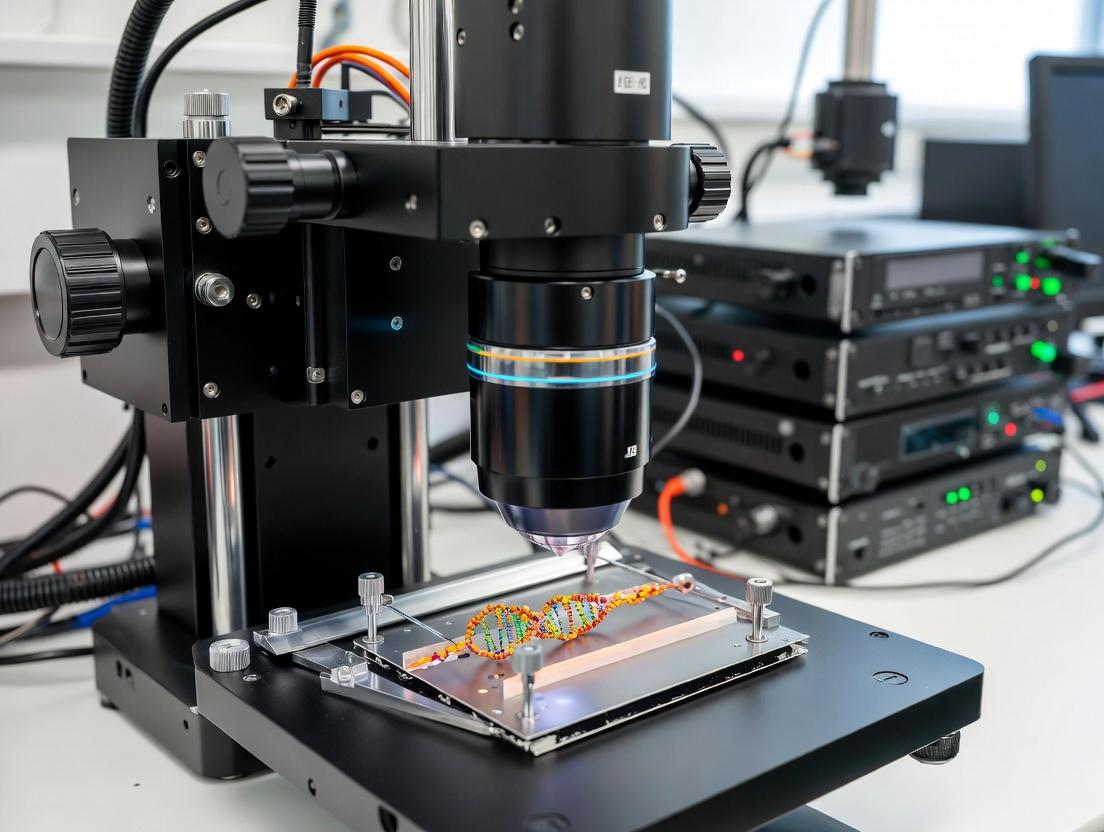
1. Introduction Within the broader thesis on characterizing Polymer-DNA nanowire morphology via Atomic Force Microscopy (AFM), this document details the standardized computational workflow required to transform raw AFM topography scans into robust, quantitative metrics. The reproducibility of dimensional analysis (e.g., height, width, contour length, persistence length) is paramount for correlating nanowire structure with its biophysical properties in drug delivery and nanofabrication research.
2. Experimental Protocols for AFM Imaging of Polymer-DNA Nanowires Protocol 2.1: Sample Preparation and Immobilization
- Substrate Treatment: Incubate freshly cleaved mica (Grade V1) in a 10 mM NiCl₂ solution for 5 minutes to create a positively charged surface. Rinse thoroughly with ultrapure water (18.2 MΩ·cm) and dry under a gentle stream of N₂ gas.
- Nanowire Deposition: Dilute the synthesized Polymer-DNA nanowire stock solution in the appropriate deposition buffer (e.g., 10 mM HEPES, pH 7.5) to a final concentration of 1-2 nM. Piper 20 µL onto the treated mica surface.
- Adsorption: Allow adsorption for 2 minutes in a humidity chamber to prevent evaporation.
- Rinsing and Drying: Gently rinse the surface with 2 mL of ultrapure water to remove unbound material and salts. Dry thoroughly under a stream of filtered N₂ gas.
Protocol 2.2: AFM Imaging Parameters (Tapping Mode in Air)
- Instrument: MultiMode AFM with a Nanoscope V controller.
- Probe: RTESPA-300 silicon probe (Bruker), nominal frequency ~300 kHz, nominal spring constant ~40 N/m.
- Scan Rate: 1.0 Hz.
- Scan Points: 512 samples per line.
- Scan Size: 2 µm x 2 µm (for overview), 1 µm x 1 µm (for high-resolution analysis).
- Setpoint Ratio: Maintained at ~0.95 to ensure minimal force application.
- Data Type: Height and Amplitude channels are recorded simultaneously.
3. Image Processing & Analysis Workflow The core software workflow is implemented using a combination of Gwyddion (open-source) and custom Python scripts, ensuring both accessibility and customizability.
Protocol 3.1: Pre-processing in Gwyddion
- Import: Open raw
.spmor.000files. - Leveling: Execute
Data → Level → Mean plane subtraction. - Scar Removal: Use
Process → Statistical → Row alignmentto correct for scan line artifacts. - Outlier Removal: Apply
Process → Outliers → Remove by maskto eliminate singular spikes. - Export: Export the leveled height data as an ASCII matrix (
.txtor.xyz) for downstream analysis.
4. Quantitative Dimensional Analysis Protocol Protocol 4.1: Contour Tracing and Length Measurement (Python-based)
- Load the pre-processed height map into a Python environment using NumPy.
- Apply a height threshold (typically 1-1.5 nm above substrate) to create a binary mask of the nanowire.
- Skeletonize the binary mask using
skimage.morphology.skeletonize. - Extract the pixel-coordinate path of the skeleton.
- Convert pixel coordinates to nanometers using the AFM scan calibration.
- Calculate the contour length (Lc) by summing the Euclidean distances between all sequential points in the path.
Protocol 4.2: Cross-Sectional Height and Width Analysis
- For each nanowire, manually or automatically define 5-10 cross-sectional lines perpendicular to its local axis.
- Extract the height profile for each line.
- Fit each profile to a Gaussian function (or two Gaussians for width).
- Extract the height (H) as the maximum of the fitted Gaussian.
- Extract the Full Width at Half Maximum (FWHM) as the width metric.
5. Data Presentation
Table 1: Summary of Quantitative Metrics from Analysis of PLL-g-DNA Nanowires (n=50)
| Metric | Mean ± SD | Protocol Used | Relevance to Morphology |
|---|---|---|---|
| Contour Length (Lc) | 452 ± 112 nm | 4.1 | Measures overall extension and flexibility. |
| End-to-End Distance (Re) | 298 ± 95 nm | 4.1 (from path endpoints) | Related to persistence length and rigidity. |
| Height (H) | 2.1 ± 0.3 nm | 4.2 | Indicates monolayer formation and compaction. |
| FWHM Width (W) | 18.5 ± 2.8 nm | 4.2 | Influenced by tip convolution and polymer chain packing. |
| Persistence Length (Lp)* | 35 ± 12 nm | Derived from ‹Re²› = 4LpLc[1 - 2Lp/Lc(1 - exp(-Lc/2Lp))] | Key metric of mechanical stiffness. |
Calculated via worm-like chain model fitting.
6. Visualization of the Computational Workflow
Title: Image Processing & Dimensional Analysis Workflow
7. The Scientist's Toolkit: Research Reagent & Material Solutions
Table 2: Essential Materials for AFM-Based Nanowire Characterization
| Item | Supplier Example | Function in Protocol |
|---|---|---|
| Muscovite Mica (V1 Grade) | Ted Pella Inc. | Provides an atomically flat, negatively charged substrate for sample adsorption. |
| Nickel(II) Chloride (NiCl₂) | Sigma-Aldrich | Used for cationic functionalization of mica to electrostatically bind DNA nanostructures. |
| HEPES Buffer | Thermo Fisher Scientific | Provides a stable, biologically compatible pH environment during nanowire deposition. |
| RTESPA-300 AFM Probes | Bruker | High-resolution tapping mode probes optimized for imaging soft biological samples in air. |
| Gwyddion (v2.65+) | Open Source | Primary software for AFM data visualization, leveling, and basic artifact correction. |
| Python SciKit-Image | Open Source | Core library for advanced image analysis (thresholding, skeletonization, measurements). |
Solving Common AFM Challenges: Artifact Identification and Optimization for Reliable Nanowire Data
Application Notes
Atomic Force Microscopy (AFM) is indispensable for characterizing the morphology of polymer-DNA nanowires, a critical system for biosensing and nanoscale electronics. Accurate measurement of nanowire diameter, height, contour length, and surface roughness is paramount. However, pervasive imaging artifacts can severely distort quantitative data, leading to erroneous conclusions about nanowire structure and assembly efficiency. This document details protocols for identifying and mitigating three critical artifacts: tip broadening, double-tip effect, and scanner drift.
1. Tip Broadening Artifact Tip broadening causes imaged features to appear wider than their true physical dimensions due to the finite size and shape of the AFM probe tip. For polymer-DNA nanowires, this results in overestimated diameters, obscuring true structural differences.
- Identification: Nanowire widths appear uniformly enlarged and do not match known specifications (e.g., from TEM or known duplex diameter of ~2 nm). Sidewalls of features appear sloping, not vertical.
- Quantitative Impact: The measured width (Wm) is related to the true feature width (Wt) and tip radius (Rt) by: Wm ≈ Wt + 2Rt. For a tip radius of 10 nm, a 2 nm DNA nanowire will be imaged as ~22 nm wide.
2. Double-Tip (Multiple-Tip) Artifact This artifact arises from a contaminated tip with multiple points of contact, producing ghost images or repeating patterns.
- Identification: Appearance of duplicate, shifted, or "shadow" features alongside real nanowires, especially prominent on isolated, high-contrast nanostructures. The artifact is often directional.
- Impact: Can be misinterpreted as bundled nanowires, braided structures, or additional nanostructures, falsely indicating aggregation or specific assembly pathways.
3. Scanner Drift Artifact Thermal or mechanical instability in the piezoelectric scanner causes distortion in the X, Y, or Z axes over time, compromising dimensional accuracy.
- Identification: Non-reproducible measurements across sequential scans, stretching or compression of features in one direction, and closing/openening of loop traces in forward vs. backward scan directions. For long, linear nanowires, drift can make them appear curved or wavy.
- Impact: Distorts contour length measurements, compresses or elongates periodic structures (e.g., beads-on-a-string morphologies), and prevents reliable correlation of specific features over time.
Data Presentation
Table 1: Summary of Artifacts, Impact on Polymer-DNA Nanowire Characterization, and Diagnostic Tests
| Artifact | Primary Impact on Measurement | Key Diagnostic Test | Typical Error Range (Example) |
|---|---|---|---|
| Tip Broadening | Overestimation of lateral dimensions (width, diameter). | Image known calibration sample (e.g., gold nanoparticles, pitch gratings). Compare height (less affected) vs. width data. | Diameter error: +50% to +500% for sub-10 nm features. |
| Double-Tip Effect | False structural interpretation (duplication, bundling). | Rotate sample 90° and re-scan. Artifact orientation relative to features will change. Image isolated, sharp test structures. | N/A (qualitative distortion) |
| Scanner Drift | Distortion of shape/length; non-reproducible metrics. | Perform sequential imaging of a fixed grid. Measure temporal evolution of feature positions. Analyze trace-retrace loop closure. | XY Drift: 0.5 - 5 nm/min (ambient); <0.2 nm/min (good stability). |
Experimental Protocols
Protocol 1: Characterization and Correction for Tip Broadening Objective: Determine effective tip geometry and apply deconvolution to obtain true nanowire dimensions.
- Tip Qualification: Prior to nanowire imaging, scan a tip characterization sample (e.g., TipCheck grating with sharp spikes or known nanoparticles). Use scan parameters identical to those planned for biological samples (soft engagement, fluid if applicable).
- Image Analysis: Use tip reconstruction software (e.g., blind tip estimation, based on the wear-less algorithm) to generate a 3D model of the tip apex from the calibration scan.
- Nanowire Imaging: Image polymer-DNA nanowires deposited on freshly cleaved mica (1-2 mM Mg²⁺ in buffer for adhesion).
- Data Deconvolution: Apply the tip model via deconvolution algorithms in the AFM software to the nanowire image. The corrected image provides a closer approximation of true topography.
- Validation: Report both raw and deconvoluted width measurements. Use height measurements, which are less susceptible to broadening, as a more reliable metric for single nanowire dimensions.
Protocol 2: Diagnosis and Remediation of Double-Tip Effect Objective: Confirm artifact and restore data integrity.
- In-Situ Diagnosis: If ghosting is suspected, immediately image a sample with well-defined, isolated sharp features (e.g., gold nanoparticles on a flat substrate or DNA origami structures).
- Directionality Test: Acquire an image, then rotate the sample by approximately 90 degrees and image the same area. A real feature will rotate with the sample; a double-tip artifact will change its orientation relative to the scan direction.
- Tip Cleaning: If artifact is confirmed:
- In Air: Use a cleaning substrate (e.g., proprietary cleaning disks, or freshly cleaved mica with adhesive) to perform several gentle scans.
- In Liquid: Retract the tip and flush the fluid cell with copious clean buffer. Engage on a clean area of mica away from the sample.
- Verification: Re-image the diagnostic sample to confirm the artifact is eliminated before returning to the nanowire sample.
Protocol 3: Monitoring and Compensating for Scanner Drift Objective: Quantify drift rates and implement strategies to minimize their impact.
- Stabilization: Allow the AFM system to thermally equilibrate for at least 45-60 minutes after loading the sample and scanner.
- Drift Measurement:
- Identify a stable, unique feature (e.g., a nanowire junction or a large particle) in a scan.
- Set the microscope to repeatedly image a small region (e.g., 500 x 500 nm) centered on this feature every 2-5 minutes for 30 minutes.
- Track the X and Y coordinates of the feature's centroid over time using particle analysis software.
- Drift Rate Calculation: Plot position vs. time. The slope of a linear fit yields the drift rate (nm/min). Acceptable thresholds are < 0.5 nm/min for high-resolution work.
- Compensation: For long-duration scans (e.g., >15 minutes), use software-based "drift compensation" features if available. For critical measurements, always perform sequential fast scans and compare, rather than relying on a single slow-scan image.
Mandatory Visualization
Diagram Title: Logical Flow for Identifying and Addressing Common AFM Artifacts
Diagram Title: Protocol Workflow for High-Fidelity Polymer-DNA Nanowire AFM
The Scientist's Toolkit
Table 2: Essential Research Reagent Solutions for Polymer-DNA Nanowire AFM
| Item | Function/Benefit | Key Consideration for Polymers & DNA |
|---|---|---|
| Ultra-Sharp AFM Probes (e.g., Si cantilevers, <10 nm tip radius) | Minimizes tip broadening artifact, enabling true nanoscale resolution of wire diameter. | Stiffness (k) must be tuned for imaging in soft tapping mode to avoid damaging nanostructures. |
| Tip Characterization Sample (e.g., sharp spike array, monodisperse Au nanoparticles) | Provides known geometry to reconstruct tip shape and quantify broadening. | Critical for any quantitative width measurement of sub-20 nm features. |
| Freshly Cleaved Mica Substrates | Provides an atomically flat, negatively charged surface for adsorbing nanowires. | Divalent cations (Mg²⁺, Ni²⁺) in deposition buffer are essential for DNA adhesion to mica. |
| Scanning Probe Image Processor (SPIP) or Gwyddion Software | Enables advanced image analysis, tip deconvolution, drift correction, and 3D rendering. | Necessary for rigorous artifact correction and extracting statistical morphological data. |
| Vibration Isolation System (active or passive) | Reduces environmental noise floor, improving resolution and minimizing pseudo-drift. | Mandatory for high-resolution imaging of flexible polymer-DNA constructs. |
| Temperature-Controlled AFM Stage (if available) | Stabilizes scanner and sample thermal equilibrium, drastically reducing scanner drift. | Particularly important for time-series or in-situ studies of nanowire formation. |
Within a thesis focused on Atomic Force Microscopy (AFM) for characterizing polymer-DNA nanowire morphology, managing tip-sample interactions is paramount. These soft, compliant nanostructures are prone to adhesion, deformation, and even displacement during imaging, leading to artifacts and unreliable data. This document outlines practical strategies and detailed protocols to minimize these interactions, enabling high-fidelity, quantitative nanoscale metrology of polymer-DNA constructs, a critical capability for advancing drug delivery and nanobiotechnology research.
Key Strategies for Reducing Interactions
| Strategy | Mechanism | Recommended Parameters/Reagents | Primary Benefit for Polymer-DNA Structures |
|---|---|---|---|
| Low-Force Imaging Modes | Minimizes vertical force. | QI, PeakForce Tapping, gentle tapping | Preserves height integrity, reduces indentation. |
| Functionalized Probes | Modifies surface chemistry. | PEG-coated tips, hydrophilic coatings | Reduces capillary & adhesive forces. |
| Liquid-Phase Imaging | Eliminates capillary forces. | Buffer (e.g., 1x TE, PBS) or solvent | Maintains native hydration state, reduces adhesion. |
| Optimized Setpoint & Drive | Lowers lateral forces. | High amplitude, low setpoint (~0.8-0.9 ratio) | Prevents sample dragging & deformation. |
| Stiffer Substrates | Provides mechanical support. | Freshly cleaved mica, AP-mica, SiO₂ | Anchors structures, reduces substrate deformation. |
| Sample Fixation (Light) | Mildly stabilizes structure. | Low concentration glutaraldehyde (<0.1%), Mg²⁺ ions | Minimal structural locking for morphology studies. |
Detailed Experimental Protocols
Protocol 1: Sample Preparation on AP-Mica for Liquid Imaging
Objective: To immobilize negatively charged polymer-DNA nanostructures with minimal non-specific adhesion.
- Substrate Preparation: Flood a freshly cleaved V-1 grade mica disk with 20-50 µL of 0.1% (v/v) 3-aminopropyltriethoxysilane (APTES) in ultrapure water for 15 minutes.
- Rinse: Thoroughly rinse the mica surface with ultpure water (3 x 1 mL) and gently dry under a stream of filtered nitrogen or argon.
- Sample Adsorption: Apply 30 µL of your polymer-DNA nanostructure solution (in 1x TE buffer + 10-50 mM NaCl or MgCl₂) onto the AP-mica for 5-10 minutes.
- Liquid Cell Loading: Rinse gently with 1 mL of the same imaging buffer (e.g., 1x TE + 10 mM MgCl₂) to remove unbound material. Immediately mount the substrate into the AFM liquid cell, ensuring no air bubbles are trapped.
Protocol 2: AFM Imaging Using PeakForce Tapping in Fluid
Objective: To acquire high-resolution topography with calibrated, sub-100 pN forces.
- Probe Selection: Use a sharp, nitride lever with a nominal spring constant (k) of 0.1 - 0.7 N/m (e.g., Bruker ScanAsyst-Fluid+ or Olympus RC800PSA).
- Calibration: Perform thermal tune in fluid to determine the exact spring constant and optical lever sensitivity.
- Parameter Setup:
- PeakForce Setpoint: Start at 100 pN, adjust downward until the tip maintains contact without deformation (target 50-150 pN range).
- Frequency: Set PeakForce Frequency to 0.5-2 kHz.
- Scan Rate: 0.5-1.0 Hz.
- Feedback Gains: Adjust to maintain a constant peak force error signal.
- Engage & Scan: Engage the probe and begin scanning a small area (e.g., 1 x 1 µm). Continuously lower the PeakForce setpoint until the morphology appears stable and reproducible over consecutive scans.
The Scientist's Toolkit: Research Reagent Solutions
| Item | Function & Rationale |
|---|---|
| APTES-functionalized Mica (AP-mica) | Creates a positively charged surface for electrostatic immobilization of DNA, preventing drift and displacement. |
| TE Buffer with Divalent Cations (MgCl₂/NiCl₂) | Provides ionic screening and promotes DNA adhesion to mica; essential for stabilizing structures in liquid. |
| PEGylated AFM Probes (e.g., biolever) | Inert, hydrophilic coating drastically reduces non-specific adhesion and hydrophobic interactions with soft polymers. |
| Gentle Glutaraldehyde Solution (0.05-0.1%) | Mild cross-linking agent for light fixation, useful for air-phase imaging of otherwise unstable 3D assemblies. |
| High-Resolution Silicon Nitride Tips (k ~0.1 N/m) | Low spring constant minimizes applied force; sharp tip (tip radius <10 nm) enhances lateral resolution. |
Visualizations
Title: AFM Force Reduction Strategy Workflow
Title: Interaction Forces & Mitigation Methods
Within the broader thesis on Atomic Force Microscopy (AFM) for polymer-DNA nanowire morphology characterization, environmental control is not merely an experimental luxury—it is a foundational requirement. The self-assembly, stability, and nanoscale architecture of polymer-DNA nanowires are profoundly sensitive to ambient humidity and temperature. Uncontrolled conditions lead to artifacts such as capillary forces, sample degradation, and inconsistent probe-sample interactions, which corrupt morphological data. These artifacts, in turn, compromise conclusions about nanowire dimensions, persistence length, and molecular packing—parameters critical for applications in biosensing, nanoelectronics, and targeted drug delivery. Therefore, precise environmental optimization is the cornerstone of reliable, reproducible nanometrology in this research domain.
The Impact of Humidity and Temperature: Quantitative Data
The following tables summarize the quantitative effects of environmental factors on AFM imaging and polymer-DNA nanowire properties, synthesized from current literature and experimental observations.
Table 1: Effects of Relative Humidity (RH) on Ambient AFM Imaging Artifacts
| RH Range (%) | Primary Effect on AFM | Impact on Polymer-DNA Nanowires | Recommended Imaging Mode |
|---|---|---|---|
| < 20% | High electrostatic charges, sample dehydration, tip/sample damage. | Dehydration-induced collapse, loss of native conformation. | Tapping Mode (TM) or PeakForce Tapping (PFT) with conductive coating. |
| 20% - 40% | Optimal Range. Minimized capillary forces, stable meniscus. | Preservation of solution-state morphology, stable adhesion. | TM or PFT. Contact Mode possible with low force. |
| 40% - 60% | Increasing capillary forces, meniscus instability, higher adhesion. | Possible swelling, increased apparent height. | TM/PFT with stricter amplitude setpoint control. |
| > 60% | Large, unstable capillary bridge, complete dominance of adhesive forces. | Severe swelling, dissolution, or diffusion of nanostructures. | Non-contact mode; environmental enclosure required. |
Table 2: Effects of Temperature on System Stability and Sample Properties
| Parameter | Effect at Lower Temperature (< 20°C) | Effect at Higher Temperature (> 25°C) | Optimal Target |
|---|---|---|---|
| Piezo Scanner Drift | Reduced thermal drift. | Increased thermal drift, reduced spatial accuracy. | 23 ± 1°C (scanner thermal equilibrium). |
| Polymer-DNA Dynamics | Slowed, may stabilize fragile constructs. | Accelerated, may promote annealing or degradation. | 20-25°C (dependent on molecular design). |
| Relative Humidity Control | Easier to maintain low RH. | Requires precise control as RH fluctuates with T. | Coupled with RH setpoint (e.g., 25°C, 30% RH). |
| Vibration Noise | Often lower due to reduced convection. | Can increase due to air currents. | Stable, scanner-matched temperature. |
Experimental Protocols for Environmental Control
Protocol 3.1: Calibration and Mapping of Local Microclimate
Objective: To characterize the actual humidity and temperature at the AFM probe-sample junction, which often differs from room conditions. Materials: Hygrometer/Thermometer with microprobe (e.g., Omega HHM290), AFM, environmental enclosure (if available). Procedure:
- Place the microprobe sensor in direct proximity to the AFM scanner head, mimicking the sample position.
- Seal the AFM with its standard acoustic hood (or environmental chamber).
- Record baseline temperature (T) and relative humidity (RH) every 30 seconds for 30 minutes to establish equilibrium.
- Introduce a localized dry or humid gas stream (e.g., using a gentle flow of N₂ or humidified air from a bubbler) near the stage while monitoring the sensor. Map the response time and gradient.
- Data Utilization: Use this calibrated microclimate data as the true environmental setpoint for all experiments, not the room readings.
Protocol 3.2: Controlled Humidity Imaging of Polymer-DNA Nanowires
Objective: To acquire high-resolution topography of polymer-DNA nanowires at a defined, stable relative humidity. Materials: AFM with active environmental controller (e.g., JedTech chamber, custom setup), silicon or silicon nitride probes (k ~ 1-40 N/m, f ~ 60-350 kHz), polymer-DNA nanowire sample on mica or AP-mica, dry N₂ gas, humidifier bubbler, mass flow controllers. Procedure:
- Sample Preparation: Deposit nanowires onto freshly cleaved mica. Allow adsorption (15-30 min). Rinse gently with ultrapure water and dry under a gentle stream of clean N₂.
- System Pre-equilibration: a. Mount the sample in the AFM scanner. b. Seal the environmental enclosure. c. Set the mass flow controllers to deliver a mixed stream of dry and humidified N₂. d. Set the target RH (e.g., 30%) and temperature (23°C) on the controller. Allow the system to stabilize for at least 45 minutes. e. Monitor the internal sensor to confirm stability (±1% RH, ±0.5°C).
- AFM Imaging: a. Engage the probe in Tapping Mode. b. Set a moderate scan rate (0.5-1.5 Hz) and low integral gain to start. c. Continuously monitor the phase signal and amplitude error. Adjust the setpoint to maintain a light tapping condition (amplitude reduction ~5-15%). d. Acquire images at multiple scan sizes (e.g., 10µm, 2µm, 500nm).
- Post-Experiment: Ramp down humidity by flowing dry N₂ before opening the chamber to prevent condensation.
Protocol 3.3: Humidity-Dependent Morphometry Experiment
Objective: To quantitatively measure the change in polymer-DNA nanowire height and width as a function of RH. Materials: As in Protocol 3.2. AFM software with section analysis and particle analysis tools. Procedure:
- Baseline Image: At 20% RH, locate and image a suitable field of nanowires (2µm x 2µm). Store this image.
- Stepwise RH Increase: Increase the RH setpoint to 30%, 40%, 50%, and 60%. At each step, allow 30 minutes for equilibration.
- Image Acquisition: At each RH step, re-image the exact same nanowires using the AFM’s image registration or offset functions.
- Quantitative Analysis: a. For each nanowire at each RH, perform 5 perpendicular section analyses to measure Full Width at Half Maximum (FWHM) and mean height. b. Plot Height vs. RH and FWHM vs. RH for individual nanowires. c. Perform statistical analysis (e.g., ANOVA) to determine if morphological changes are significant.
Visualization: Workflows and Relationships
Diagram Title: Environmental Control Impact on AFM Thesis Outcomes
Diagram Title: Ambient AFM Environmental Control Workflow
The Scientist's Toolkit: Research Reagent Solutions
Table 3: Essential Materials for Environmental AFM of Polymer-DNA Nanowires
| Item Name | Function/Benefit | Critical Specification/Example |
|---|---|---|
| Active Environmental Chamber | Seals the scanner, actively controls and monitors RH and T via feedback loops. | JedTech Humidifier/Dehumidifier system; custom chamber with PID control. |
| Mass Flow Controllers (MFCs) | Precisely mix dry and humid gas streams to achieve target RH. | Two-channel MFC (e.g., Alicat), range 0-500 sccm. |
| Ultra-Pure Water Humidifier | Generates humid gas stream without contaminants. | In-house bubbler with 18.2 MΩ·cm water, 0.22µm filtered gas input. |
| Inert Dry Gas Source | Provides dry carrier gas (N₂ or Ar) to prevent oxidation and control baseline RH. | High-purity N₂ tank with moisture trap (<1% RH output). |
| Calibrated Micro-Sensor | Measures the true microclimate at the probe-sample junction. | Calibrated hygrometer/thermometer with fine probe (e.g., Honeywell HIH8000). |
| AP-mica or APS-treated Substrates | Provides strong, covalent adhesion for nanowires, preventing displacement during humidity changes. | (3-Aminopropyl)triethoxysilane (APTES) functionalized mica. |
| Humidity-Stable AFM Probes | Probes with consistent mechanical properties across RH changes. | Gold-coated Si probes for reduced electrostatic charge; low spring constant (~1-5 N/m). |
| Vibration Isolation System | Mitigates low-frequency noise exacerbated by air currents from environmental control. | Active or passive isolation table, acoustic hood. |
1. Introduction In the context of characterizing polymer-DNA nanowire morphology via Atomic Force Microscopy (AFM), sample preparation is critical. Poor adsorption of nanowires to the substrate leads to sparse imaging data, while excessive aggregation obscures individual morphology. This note details surface functionalization and buffer optimization strategies to achieve optimal, homogeneous dispersion for reliable AFM analysis.
2. Surface Functionalization Protocols The goal is to modify substrate surface charge to electrostatically attract and immobilize negatively charged polymer-DNA nanowires.
Protocol 2.1: APTES Silanization for Aminated (Positively Charged) Surfaces
- Materials: Clean silicon wafer or mica, (3-Aminopropyl)triethoxysilane (APTES), anhydrous toluene, ethanol.
- Procedure:
- Plasma clean substrate for 5 minutes.
- Prepare a 2% (v/v) solution of APTES in anhydrous toluene.
- Immerse the substrate in the APTES solution for 1 hour at room temperature under nitrogen atmosphere.
- Rinse sequentially with toluene, ethanol, and ultrapure water (3x each).
- Cure at 110°C for 15 minutes. Store under nitrogen.
- Mechanism: APTES forms a self-assembled monolayer, presenting primary amine groups (NH₃⁺ at neutral pH) for electrostatic binding with DNA phosphate backbone.
Protocol 2.2: Poly-L-Lysine (PLL) Coating for Rapid Positively Charged Surfaces
- Materials: Freshly cleaved mica, Poly-L-Lysine solution (0.1% w/v in water).
- Procedure:
- Apply 20 µL of 0.1% PLL solution onto the center of a freshly cleaved mica disk.
- Incubate for 5 minutes.
- Rinse gently but thoroughly with 2 mL of ultrapure water to remove unbound PLL.
- Dry under a gentle stream of nitrogen or argon.
Protocol 2.3: Mg²⁺-Assisted Adsorption on Mica (Divalent Cation Bridge)
- Materials: Freshly cleaved mica, Magnesium acetate or MgCl₂.
- Procedure:
- Prepare a 10 mM solution of magnesium acetate in ultrapure water.
- Apply 20 µL of the magnesium solution onto mica.
- Immediately add 5-10 µL of your polymer-DNA nanowire sample directly into the droplet and incubate for 2-5 minutes.
- Rinse with ultrapure water (2 mL) and dry gently. Note: Optimal Mg²⁺ concentration is sample-dependent.
3. Buffer and Solution Optimization Buffer composition directly influences nanowire conformation and aggregation state.
Key Parameters:
- Salt Type & Concentration: Low ionic strength (<10 mM monovalent salt) can minimize aggregation but may reduce adsorption. Divalent cations (Mg²⁺) promote adsorption but can cause aggregation at high concentrations.
- pH: Must be optimized for both surface charge and nanowire stability. Typically pH 7.5-8.5 for DNA-based structures.
- Additives: Surfactants (e.g., Tween-20) or crowding agents (e.g., glycerol) can modulate dispersion.
Protocol 3.1: Systematic Buffer Screening for Deposition
- Prepare your polymer-DNA nanowire sample in the following buffers:
- TE Buffer (10 mM Tris-HCl, 1 mM EDTA, pH 8.0)
- Tris-Acetate (10 mM, pH 8.0)
- HEPES (10 mM, pH 7.5)
- Tris-HCl (10 mM) + 1-10 mM MgCl₂ (gradient)
- Tris-HCl (10 mM, pH 8.0) + 0.01% Tween-20
- Follow a standard deposition protocol (e.g., Protocol 2.3) for each buffer condition.
- Image multiple areas via AFM and quantify surface coverage and aggregation index.
- Prepare your polymer-DNA nanowire sample in the following buffers:
4. Quantitative Data Summary
Table 1: Comparison of Surface Functionalization Methods
| Method | Mechanism | Optimal For | Advantages | Disadvantages | Typical Coverage* |
|---|---|---|---|---|---|
| APTES | Covalent amine layer | Long-term stable surfaces | Very stable, reusable | Multi-step, requires anhydrous conditions | 40-70% |
| Poly-L-Lysine | Electrostatic polymer coating | Quick screening | Fast, simple, high positive charge density | Can be too "sticky," may promote aggregation | 60-90% |
| Mg²⁺ on Mica | Divalent cation bridge | DNA-rich nanostructures | Preserves native conformation, very clean | Concentration-sensitive, can cause aggregation | 30-80% |
*Coverage % is highly sample-dependent. Values represent typical ranges for well-dispersed 100-500 nm polymer-DNA nanowires.
Table 2: Effect of Deposition Buffer on Morphology & Aggregation
| Buffer Composition | Adsorption Efficacy | Observed Aggregation | Recommended Use Case |
|---|---|---|---|
| 10 mM Tris, 1 mM EDTA (TE) | Low | Very Low | For stable, charge-shielded structures prone to aggregation. |
| 10 mM Tris, 5 mM MgCl₂ | Very High | Moderate-High | For stubborn adsorption; requires optimization of [Mg²⁺]. |
| 10 mM HEPES, pH 7.5 | Moderate | Low | Good general-purpose buffer for physiological pH. |
| 10 mM Tris, 0.01% Tween-20 | Moderate-Low | Very Low | Critical for samples with high hydrophobic character. |
5. The Scientist's Toolkit: Research Reagent Solutions
| Item | Function in Experiment |
|---|---|
| Freshly Cleaved Mica | Atomically flat, negatively charged substrate. The standard for high-resolution AFM of biomolecules. |
| (3-Aminopropyl)triethoxysilane (APTES) | Silane coupling agent to create a reproducible, positively charged amine surface on silicon/glass. |
| Poly-L-Lysine Solution (0.1%) | Positively charged polymer for rapid, electrostatic coating of mica or glass. |
| Magnesium Acetate (Mg(OAc)₂) | Source of Mg²⁺ ions. Acetate is less corrosive than chloride for AFM tips. Creates cation bridge. |
| Ultrapure Water (nuclease-free) | Prevents contamination and unwanted degradation of DNA components during rinsing/buffer prep. |
| Tween-20 (Polysorbate 20) | Non-ionic surfactant to reduce hydrophobic interactions and non-specific aggregation. |
| Tris-EDTA (TE) Buffer | Common DNA storage buffer. EDTA chelates divalent cations to prevent nuclease activity and aggregation. |
6. Visualization of Strategy and Workflow
Troubleshooting Strategy Decision Tree
Polymer-DNA Nanowire AFM Prep Workflow
This application note details the protocol for Liquid-Phase Atomic Force Microscopy (LP-AFM), a critical technique within a broader thesis investigating the morphology of polymer-DNA nanowires for biosensing and nanoelectronic applications. Traditional AFM imaging in air often introduces artifacts due to sample dehydration and high tip-sample adhesion forces, which can distort the soft, dynamic structures of biopolymer hybrids. LP-AFM enables characterization in a near-native, hydrated state, preserving intrinsic morphology and enabling the observation of dynamic processes. This is indispensable for accurately correlating the structure of polymer-DNA nanowires with their function in proposed drug delivery or diagnostic platforms.
Key Advantages and Quantitative Comparison
Table 1: Comparative Performance of Air vs. Liquid-Phase AFM for Soft Samples
| Parameter | Air-Phase AFM | Liquid-Phase AFM | Implication for Polymer-DNA Nanowires |
|---|---|---|---|
| Adhesion Force | High (5-50 nN) | Low (0.1-1 nN) | Prevents nanowire deformation and tip-induced aggregation. |
| Resolution | ~0.5 nm (lateral) | ~1.0 nm (lateral) | Slightly reduced but more biologically accurate. |
| Sample Dehydration | Significant | Minimized | Preserves hydration shell and 3D conformation of DNA segments. |
| Imaging Mode | Primarily Tapping | Tapping & Contact | Enables stable contact-mode imaging for conductivity mapping. |
| Environmental Control | Limited | Tunable buffer, pH, temperature | Allows real-time observation of assembly/disassembly kinetics. |
Detailed Experimental Protocol: LP-AFM of Polymer-DNA Nanowires
Protocol 3.1: Substrate Preparation (Mica Functionalization)
- Cleave: Obtain a fresh, atomically flat surface by cleaving muscovite mica with adhesive tape.
- Functionalize: Deposit 20 µL of 0.1% (w/v) poly-L-lysine (PLL) solution onto the mica for 5 minutes.
- Rinse: Gently rinse the mica with 2 mL of ultrapure water (18.2 MΩ·cm) to remove unbound PLL.
- Dry: Use a gentle stream of dry, filtered nitrogen or argon to dry the substrate. The positively charged PLL layer promotes adhesion of negatively charged DNA strands.
Protocol 3.2: Sample Deposition and Incubation
- Dilute: Dilute the synthesized polymer-DNA nanowire solution in the desired imaging buffer (e.g., 10 mM HEPES, 5 mM MgCl₂, pH 7.5) to a final DNA concentration of 1-5 nM.
- Deposit: Pipette 30 µL of the diluted sample onto the center of the PLL-functionalized mica.
- Incubate: Allow adsorption to proceed for 10 minutes in a humid chamber to prevent evaporation.
- Wash: Carefully introduce 2 mL of imaging buffer to the sample droplet to remove loosely bound material. Do not let the substrate dry.
Protocol 3.3: Liquid Cell Assembly and Imaging
- Assemble: Mount the substrate onto the AFM sample disk. Seal the O-ring of the liquid cell and carefully lower the cantilever holder assembly.
- Inject: Using a syringe, slowly inject imaging buffer into the liquid cell until it is fully purged of air.
- Thermalize: Allow the system to thermally equilibrate for 15 minutes to minimize drift.
- Engage: Engage the tip in fluid using standard procedures, typically with a setpoint of 0.5-1.0 V and a drive frequency ~5-10% below the in-liquid resonance frequency.
- Image: Scan at a rate of 1-2 Hz with 512x512 pixel resolution. Continuously adjust gains and setpoint for optimal stability.
Visualization: LP-AFM Workflow
Diagram 1: LP-AFM for Near-Native Imaging Workflow (100 chars)
The Scientist's Toolkit: Essential Research Reagents & Materials
Table 2: Key Reagent Solutions for LP-AFM of Polymer-DNA Nanowires
| Item | Function & Specification |
|---|---|
| Muscovite Mica (V1 Grade) | Atomically flat, negatively charged substrate for sample deposition. |
| Poly-L-Lysine (PLL) Solution (0.1% w/v) | Creates a positively charged adhesion layer on mica for nucleic acid immobilization. |
| HEPES Buffer (10 mM, pH 7.5) | Biologically relevant, non-coordinating buffer for imaging. Maintains pH stability. |
| MgCl₂ (5-10 mM) | Divalent cation source. Promotes DNA adhesion to mica/PLL by shielding negative charges. |
| Liquid AFM Cantilevers (SNL/OMCL-RC800) | Silicon nitride tips with low spring constant (~0.1 N/m) for soft tapping in fluid. |
| Syringe Filter (0.22 µm, PES) | For sterile filtration of all buffers to eliminate particulate contaminants. |
| Precision Syringe (1 mL) | For bubble-free injection of imaging buffer into the sealed liquid cell. |
Beyond AFM: Validating Morphology with Complementary Techniques for Complete Nanoscale Analysis
This application note details protocols for the correlative microscopy of polymer-DNA nanowires, a critical methodology within a broader thesis investigating the morphology of these hybrid nanostructures for drug delivery applications. Atomic Force Microscopy (AFM) provides excellent topological and mechanical data in ambient or liquid conditions but lacks internal structural resolution and can suffer from tip convolution artifacts. Transmission and Scanning Electron Microscopy (TEM/SEM) offer high-resolution internal and surface imaging but require vacuum conditions and conductive coatings that can introduce artifacts. Cross-correlation validates dimensional accuracy and structural integrity, essential for researchers and drug development professionals who require reliable nanoscale metrology to link structure to function.
Key Comparative Data: AFM vs. SEM/TEM
Table 1: Comparison of Metrology Data for Polyethyleneimine-DNA Nanowires (n=50)
| Metric | AFM (Tapping Mode, Air) | SEM (2 nm Au/Pd, 5 kV) | TEM (Negative Stain, 80 kV) | Notes |
|---|---|---|---|---|
| Avg. Diameter (nm) | 8.5 ± 2.1 | 7.1 ± 1.8 | 6.8 ± 1.5 | AFM overestimates due to tip convolution. |
| Avg. Length (nm) | 1020 ± 150 | 980 ± 120 | 970 ± 115 | Good agreement for length measurements. |
| Surface Roughness (Rq in nm) | 1.2 ± 0.3 | N/A | N/A | SEM/TEM not typically used for roughness quantification. |
| Internal Structure | Not Resolved | Surface Only | Core-Shell Contrast Visible | TEM reveals DNA condensation uniformity. |
| Sample Preparation Artifact | Minimal (air-dry) | Potential shrinkage from dehydration & coating | Potential flattening on grid |
Table 2: Suitability for Polymer-DNA Nanowire Characterization
| Characterization Need | Primary Tool | Correlative Cross-Check | Rationale |
|---|---|---|---|
| 3D Height & Mechanical Properties | AFM | SEM for contour length | AFM is unique for height and modulus. |
| Absolute Diameter Validation | TEM | AFM for general shape | TEM provides highest lateral resolution. |
| Internal Morphology & Hybrid Integrity | TEM | N/A | TEM is indispensable for core-shell assessment. |
| High-Throughput Surface Imaging | SEM | AFM on selected areas | SEM faster for large-area surveys. |
Experimental Protocols
Protocol 3.1: Correlative AFM-SEM/TEM Workflow for Polymer-DNA Nanowires
Aim: To image the same individual nanowires using multiple techniques for direct comparison.
Materials:
- Polymer-DNA nanowire suspension (e.g., PEI-plasmid DNA complexes in 10 mM HEPES buffer).
- AFM Substrate: Freshly cleaved mica (highly flat, negatively charged).
- SEM/TEM Substrate: Silicon wafer with patterned alphanumeric grid (e.g., SPI Supplies #6392).
- TEM Grid: Continuous carbon film on 400 mesh copper grid (glow-discharged for hydrophilicity).
- Negative Stain: 2% Uranyl acetate or 1% Phosphotungstic acid.
- Conductive Coating: Iridium or Au/Pd (2-3 nm) for SEM.
Procedure:
- Substrate Preparation: Cleave mica and plasma-clean the silicon grid wafer.
- Sample Deposition (Correlative):
- Apply a 5 µL droplet of nanowire suspension onto the center of the patterned silicon wafer. Incubate 2 min.
- Rinse gently with 1 mL deionized water, blot edge.
- Dry under a gentle stream of filtered nitrogen or argon.
- Initial AFM Imaging:
- Mount the silicon wafer on an AFM stub.
- Perform tapping mode AFM in air to locate nanowires within a specific grid square (e.g., C7).
- Capture high-resolution images (512x512 pixels, 1 µm scan size). Record the precise X,Y stage coordinates of features of interest.
- Critical: Use a soft tip (k ~5-40 N/m) and low amplitude setpoint to minimize sample displacement.
- Post-AFEM Processing for SEM:
- Carefully transfer the wafer to a sputter coater.
- Apply a thin (~2 nm) conductive coating of Iridium.
- SEM Imaging:
- Load the wafer into the SEM.
- Navigate to the same grid square (C7) and use the recorded AFM coordinates to locate the same nanowires.
- Image at low kV (3-5 kV) to minimize beam damage and improve surface detail.
- Parallel TEM Sample Preparation:
- Apply a 5 µL droplet of the same nanowire suspension onto a glow-discharged TEM grid. Incubate 1 min.
- Wick away excess liquid with filter paper.
- Immediately apply a 5 µL droplet of negative stain. Incubate 30 sec, then wick away and air dry.
- TEM Imaging:
- Image at 80-100 kV.
- Measure diameters and internal contrast directly from TEM images. These values serve as the "ground truth" for cross-checking AFM width measurements.
Protocol 3.2: AFM Tip Characterization for Deconvolution
Aim: To quantify and correct for AFM tip-broadening effects.
- Image a characterized tip-check sample (e.g., TGT1 grating with sharp spikes) before and after nanowire imaging.
- Use scanning electron microscopy of the AFM tip itself post-experiment to measure tip radius.
- Apply deconvolution algorithms (e.g., Blind Tip Reconstruction) using open-source software (Gwyddion) to estimate true nanowire width from AFM topographic data.
Visualization: Experimental Workflow & Data Correlation
Diagram Title: Correlative AFM-SEM-TEM Workflow for Nanowires
Diagram Title: Data Correlation Logic for Width Validation
The Scientist's Toolkit: Essential Research Reagents & Materials
Table 3: Key Research Reagent Solutions for Correlative Microscopy
| Item & Example Product | Function in Protocol | Critical Notes |
|---|---|---|
| Patterned SEM Substrate (e.g., Silicon Wafer with Finder Grid) | Enables precise relocation of the same nanowire between AFM and SEM. | Ensure grid markings are readable in both optical microscope (AFM) and SEM. |
| Freshly Cleaved Mica Discs (e.g., V1 Grade, 10mm) | Provides an atomically flat, negatively charged surface for AFM control experiments. | Essential for assessing deposition uniformity without substrate roughness. |
| Continuous Carbon TEM Grids (e.g., 400 mesh Copper) | Support film for high-resolution TEM. Glow discharge makes it hydrophilic for even sample adhesion. | Avoid holey carbon for this application to prevent nanowires spanning holes. |
| Negative Stain (2% Uranyl Acetate) | Enhances contrast in TEM by embedding and outlining the nanowire, revealing core-shell structure. | Handle as radioactive waste; Phosphotungstic acid is a non-radioactive alternative. |
| Conductive Sputter Coating Target (Iridium or Gold/Palladium) | Applied as an ultra-thin layer to render non-conductive polymer-DNA nanowires conductive for SEM. | Iridium provides finer grain size than Au/Pd for higher resolution. |
| Soft AFM Probes (e.g., Tap150Al-G, k ~5 N/m) | Used for tapping mode AFM on soft biological/polymer samples to minimize deformation and displacement. | Critical for imaging before SEM coating to avoid sweeping nanowires away. |
| Polymer-DNA Nanowire Buffer (e.g., 10 mM HEPES, pH 7.4) | Suspension buffer that maintains nanowire stability and integrity during deposition. | Avoid high-salt buffers (e.g., PBS) for AFM as they leave crystalline deposits upon drying. |
Application Notes
In the context of characterizing polymer-DNA nanowire morphology via Atomic Force Microscopy (AFM), relying solely on surface-deposited images can be misleading. Aggregation during sample preparation, surface-binding biases, and the inherent drying process can distort the true solution-state properties of the nanostructures. This protocol details the integration of Dynamic Light Scattering (DLS) and Size Exclusion Chromatography (SEC) to guide and validate AFM analysis, providing a holistic view of dispersion quality and hydrodynamic size.
- DLS provides a rapid, ensemble measurement of the hydrodynamic diameter (Dh) and a qualitative assessment of the polydispersity index (PdI) directly in solution. A low PdI (<0.2) suggests a monodisperse sample, indicating that AFM images should reveal consistent nanowire dimensions. A high PdI (>0.3) warns of aggregation or a mixed population, which must be accounted for when interpreting AFM micrographs.
- SEC separates species based on their hydrodynamic volume in solution, offering a size-distribution profile and the ability to collect fractions for further analysis. SEC validates the DLS PdI, identifies the presence of small aggregates or free polymer/DNA, and allows for the isolation of monodisperse fractions for pristine AFM characterization.
Table 1: Comparative Overview of DLS, SEC, and AFM for Nanowire Characterization
| Technique | Measured Parameter | Sample State | Key Output for Integration | Informs AFM Analysis By: |
|---|---|---|---|---|
| Dynamic Light Scattering (DLS) | Hydrodynamic Diameter (Dh), Polydispersity Index (PdI) | Solution (native state) | Z-Average Dh (nm), PdI value | Warning of aggregation (high PdI), providing expected size range in solution. |
| Size Exclusion Chromatography (SEC) | Hydrodynamic Volume, Relative Size Distribution | Solution (eluting) | Elution profile (UV/VIS/RI), fraction collection | Confirming dispersion quality, isolating monodisperse fractions, identifying contaminant peaks. |
| Atomic Force Microscopy (AFM) | Physical Dimensions (Height, Length), Morphology | Dry/Ambient on substrate | Topography image, cross-sectional analysis | Providing ground-truth dimensions; data is validated against solution-phase Dh and SEC profile. |
Protocols
Protocol 1: Pre-AFM Screening via DLS Objective: To assess the solution-state aggregation status and approximate hydrodynamic size of polymer-DNA nanowire samples prior to deposition for AFM. Materials: Purified polymer-DNA nanowire sample in appropriate buffer (e.g., 1x TE or PBS), DLS instrument (e.g., Malvern Zetasizer). Procedure:
- Sample Preparation: Filter the nanowire dispersion using a 0.45 µm or 0.1 µm syringe filter (material compatible with sample) directly into a clean, low-volume quartz cuvette or disposable sizing cell.
- Instrument Equilibration: Allow the sample to thermally equilibrate in the instrument chamber at 25°C for 300 seconds.
- Measurement Setup: Set the measurement angle to 173° (backscatter). Define the material's refractive index (e.g., 1.45) and absorption coefficient (e.g., 0.001).
- Data Acquisition: Perform a minimum of 12 sequential measurements per sample. Set automatic attenuation selection and position adjustment.
- Analysis: Use the instrument software to calculate the intensity-weighted size distribution, Z-Average Dh, and PdI. Critical Interpretation: A single, narrow peak with PdI < 0.25 suggests a sample suitable for direct AFM. A broad peak or multiple peaks indicates the need for SEC purification prior to AFM.
Protocol 2: SEC Fractionation for Monodisperse AFM Samples Objective: To separate and collect monodisperse fractions of polymer-DNA nanowires based on hydrodynamic volume. Materials: SEC system (e.g., ÄKTA pure) with appropriate column (e.g., Superose 6 Increase 10/300 GL for 1-100 nm range), running buffer (e.g., 1x PBS, 0.5 M NaCl), nanowire sample (100-500 µL, 0.5-2 mg/mL), fraction collector. Procedure:
- System Preparation: Equilibrate the SEC column with at least 1.5 column volumes (CV) of filtered (0.22 µm) and degassed running buffer at a flow rate of 0.3-0.5 mL/min.
- Sample Injection: Centrifuge the nanowire sample at 14,000 x g for 10 minutes to pellet any large aggregates. Carefully load the supernatant into the injection loop.
- Chromatographic Run: Inject the sample and initiate isocratic elution with running buffer. Monitor the eluent at 260 nm (DNA) and 280 nm (protein/polymer). Begin fraction collection (0.5-1 mL per fraction) at the void volume.
- Peak Selection: Based on the chromatogram, pool fractions corresponding to the main, symmetric peak (believed to be monodisperse nanowires). Avoid the tails of the peak.
- Sample Concentration: Concentrate the pooled SEC fraction using an appropriate molecular weight cut-off (MWCO) centrifugal concentrator (e.g., 30k or 100k MWCO) to a volume suitable for AFM deposition (~10-20 µL).
Protocol 3: Integrated AFM Sample Preparation & Analysis Objective: To deposit SEC-fractionated/DLS-characterized nanowires for correlated morphology and size analysis. Materials: Freshly cleaved mica substrate, cation solution (e.g., 10 mM NiCl2 or MgCl2), AFM with tapping mode probes (e.g., RTESPA-150). Procedure:
- Substrate Functionalization: Apply 30 µL of 10 mM NiCl2 to a freshly cleaved mica disk for 2 minutes. Rinse gently with 1 mL ultrapure water and dry under a stream of filtered nitrogen or argon.
- Sample Deposition: Dilute 2 µL of the concentrated SEC fraction into 18 µL of the corresponding SEC running buffer. Pipette this 20 µL solution onto the functionalized mica. Allow to adsorb for 5 minutes.
- Rinsing and Drying: Gently rinse the mica surface with 1 mL ultrapure water to remove salts and unbound material. Dry thoroughly under a stream of filtered inert gas.
- AFM Imaging: Mount the sample and engage a sharp tapping-mode probe. Acquire images (typically 2x2 µm to 5x5 µm) at a resolution of 512x512 pixels. Scan multiple areas to ensure representative sampling.
- Data Correlation: Measure the height and contour length of individual nanowires from AFM cross-sections. Compare the average height (diameter) from AFM to the Dh from DLS. The AFM height should be smaller than Dh due to dehydration and flattening. Consistency between the two measurements and a narrow size distribution in AFM confirm the solution-phase data.
The Scientist's Toolkit: Essential Research Reagents & Materials
| Item | Function in Protocol |
|---|---|
| 0.1 µm PVDF Syringe Filter | Removes dust and large aggregates from nanowire samples for DLS, preventing artifacts. |
| Low-Volume Disposable Sizing Cuvette | Holds minimal sample volume (12-50 µL) for DLS measurement of precious nanowire samples. |
| Superose 6 Increase 10/300 GL Column | SEC column optimized for separation of macromolecules and nanoparticles with hydrodynamic radii from 1-100 nm. |
| 30k MWCO Centrifugal Concentrator | Concentrates dilute SEC fractions to the required volume and concentration for AFM deposition. |
| Freshly Cleaved Mica Disks | Provides an atomically flat, negatively charged substrate for nanowire immobilization. |
| Nickel(II) Chloride (NiCl2) Solution | Divalent cation solution that bridges negatively charged mica and DNA/polymer, enhancing adsorption. |
| RTESPA-150 Tapping Mode AFM Probe | High-resolution probe with a sharp tip and moderate spring constant for imaging soft biological nanostructures. |
Diagram: Integrated Characterization Workflow
Application Notes
This protocol details the application of correlative Atomic Force Microscopy (AFM) with X-ray Photoelectron Spectroscopy (XPS) or Fourier-Transform Infrared Spectroscopy (FTIR) for the surface analysis of polymer-DNA nanowires. In the context of a broader thesis on AFM for nanobiomaterial characterization, this integrated approach is critical for establishing a direct link between nanoscale morphological features (e.g., wire continuity, height, surface roughness) and localized chemical composition (e.g., polymer conjugation efficiency, DNA surface coverage, presence of contaminants). This validation is essential for researchers developing these nanowires for applications in biosensing, targeted drug delivery, and nanoelectronics.
AFM provides unparalleled topographical data but lacks definitive chemical identification. XPS offers quantitative elemental and chemical state analysis from the top 5-10 nm of a surface, while FTIR provides molecular fingerprinting through vibrational spectroscopy, with attenuated total reflection (ATR) mode probing depths up to ~2 µm. By applying these techniques to the same or sequentially mapped sample regions, one can correlate specific topographic features with chemical signatures, answering questions critical to drug development: Has the polymer correctly grafted to the DNA template? Is the functional ligand present on the nanowire surface? What is the purity of the fabricated nanostructure?
Table 1: Comparison of Complementary Surface Analysis Techniques
| Technique | Probing Depth | Spatial Resolution | Key Output | Primary Role in Polymer-DNA Nanowire Analysis |
|---|---|---|---|---|
| AFM | Surface topology | ~1 nm (lateral) | Topography, roughness, mechanical properties | Maps nanowire morphology, diameter, height, and assembly uniformity. |
| XPS | 5-10 nm | 10-200 µm (micro-XPS: ~10 µm) | Elemental composition, chemical bonding states | Quantifies elemental ratios (C, N, O, P), confirms DNA (via P2p signal) and polymer-specific bonds. |
| ATR-FTIR | 0.5-2.0 µm | 10-250 µm (IR microscopy) | Molecular functional groups, vibrational modes | Identifies organic functional groups (e.g., amide, ester, carbonyl) from polymer and DNA backbone. |
Table 2: Representative Quantitative Data from Correlative Analysis of a PEG-DNA Nanowire
| Analysis Target | AFM Result | XPS Result | FTIR Result | Correlative Conclusion |
|---|---|---|---|---|
| DNA Coverage | Nanowire height: 2.1 ± 0.3 nm | Atomic % P: 3.5% (P2p peak at 133.5 eV) | Peak at 1220 cm⁻¹ (PO₂⁻ symmetric stretch) | Height and phosphorus signal confirm monolayer DNA wire formation. |
| PEG Grafting | Increased height to 5.8 ± 0.5 nm; Altered surface roughness | Increase in C-O bond % (C1s peak at 286.5 eV); O/C ratio increased by 45% | Strong C-O-C stretch at 1100 cm⁻¹; New C=O stretch at 1730 cm⁻¹ | Chemical signals from increased height confirm successful PEGylation. |
| Contaminant Detection | Particulate debris (~50 nm dia.) on substrate | Localized Na 1s peak on debris | N/A | Debris is ionic salt crystalloid, not organic contaminant. |
Experimental Protocols
Protocol 1: Sequential AFM-XPS/FTIR Analysis on Silicon Wafer Substrates
Objective: To characterize the chemical composition corresponding to specific topographic features of polymer-DNA nanowires deposited on a silicon wafer.
Materials & Substrate Prep:
- Substrate: Prime-grade, polished P-type Silicon (100) wafer.
- Sample Deposition: Deposit 10 µL of purified polymer-DNA nanowire solution (in 10 mM Tris-EDTA buffer) onto a clean, UV-ozone treated Si wafer for 2 minutes. Rinse gently with deionized water and dry under a stream of ultrapure N₂.
Procedure: Step A: AFM Topographical Mapping.
- Mount the sample on the AFM metal puck using a double-sided adhesive tab.
- Using a suitable AFM mode (e.g., Tapping Mode in air or PeakForce Tapping), image multiple large-area scans (e.g., 50 µm x 50 µm) to locate nanowire networks.
- Acquire high-resolution images (e.g., 5 µm x 5 µm, 512 x 512 pixels) of regions of interest (ROIs). Record precise stage coordinates or use fiduciary markers.
- Extract quantitative data: Section analysis for height/width, root-mean-square (RMS) roughness.
Step B: Transfer and Spectral Analysis.
- For XPS: Transfer the sample directly to the XPS load lock. Acquire survey spectra from the ROI (if using imaging XPS) or from the general sample area. Perform high-resolution scans on C1s, O1s, N1s, and P2p regions. Use a flood gun for charge neutralization.
- For ATR-FTIR: Place the Si wafer directly onto the ATR crystal (e.g., diamond), ensuring good optical contact. Acquire background spectrum on a clean Si wafer. Acquire sample spectrum (64-128 scans, 4 cm⁻¹ resolution). For micro-FTIR, locate the ROI using the visible camera and acquire transmission/reflection maps.
Step C: Data Correlation.
- Overlay chemical maps (XPS elemental maps or FTIR functional group maps) with the AFM topography image using software (e.g., Gwyddion, SPIP, or instrument vendor software) by aligning distinct, recognizable features.
Protocol 2:In-SituLiquid AFM Coupled with Ex-Situ FTIR for Dynamic Modification Studies
Objective: To monitor morphological changes during a surface reaction (e.g., enzyme digestion) and subsequently validate the chemical change.
Procedure:
- Initial AFM in Liquid: Immobilize DNA nanowires on a freshly cleaved mica substrate functionalized with 3-aminopropyltriethoxysilane (APTES). Image in buffer solution to establish baseline morphology.
- In-Situ Reaction: Introduce a solution of enzyme (e.g., DNase I) or chemical agent into the AFM liquid cell. Acquire time-lapse images at the same location to monitor topographical degradation or alteration.
- Post-Reaction Analysis: Carefully rinse the sample and dry. Transfer the exact same mica sheet to the ATR-FTIR.
- FTIR Validation: Compare the IR spectra of the reacted region to a control region. The degradation of DNA will be indicated by a reduction in the phosphate backbone signals (1220-1080 cm⁻¹) and nucleobase absorbances.
The Scientist's Toolkit: Research Reagent Solutions
| Item | Function in Polymer-DNA Nanowire Characterization |
|---|---|
| UV-Ozone Cleaner | Generates a clean, hydrophilic surface on Si/SiO₂ substrates by removing organic contaminants, ensuring uniform nanowire adsorption. |
| APTES-Silanized Mica | Provides a positively charged surface for strong electrostatic immobilization of negatively charged DNA nanowires for stable AFM imaging in liquid. |
| Anhydrous Toluene | Solvent used for silanization reactions to functionalize substrates for specific chemical binding of nanowires. |
| Certified XPS Calibration Standards (e.g., Au foil for Au 4f7/2, Cu foil for Cu 2p3/2) | Essential for precise binding energy scale calibration of the XPS instrument, ensuring accurate chemical state identification. |
| ATR-FTIR Crystal Cleaner Kit (e.g., methanol, isopropanol, lint-free wipes) | Maintains the ATR crystal free of residues from previous samples, preventing spectral contamination and ensuring quantitative accuracy. |
Visualization Diagrams
Title: Correlative AFM-XPS/FTIR Workflow for Nanowire Validation
Title: Sequential AFM to XPS/FTIR Experimental Protocol
Within the broader thesis on Atomic Force Microscopy (AFM) for characterizing polymer-wrapped DNA nanowire morphology, achieving statistically robust conclusions is paramount. Variations in polymer self-assembly, DNA-polymer interactions, and AFM tip-sample artifacts necessitate rigorous statistical design. This Application Note provides protocols for determining adequate sample sizes and implementing automated analysis pipelines to ensure reproducible, publication-quality data on nanowire height, contour length, persistence length, and surface roughness.
Determining Sample Size for AFM-Based Morphometry
Sample size must be calculated a priori to ensure sufficient statistical power to detect biologically or materially relevant effect sizes. For AFM morphometry, key parameters include mean height (nm), contour length (µm), and surface roughness (Rq, nm).
Power Analysis Protocol:
- Define Primary Endpoint: Select a single, quantifiable primary morphological metric (e.g., mean nanowire height).
- Pilot Study: Image 10-15 nanowires from at least 3 independent preparation batches. Calculate the mean and standard deviation (SD) for your primary endpoint.
- Set Effect Size: Determine the minimum difference (effect size) you consider scientifically significant (e.g., a 0.5 nm change in height due to a drug binding event).
- Choose Statistical Parameters:
- Significance Level (α): Typically 0.05.
- Statistical Power (1-β): Typically 0.80 or 0.90.
- Calculate Sample Size (n): Use the formula for comparing two independent means:
n = 2 * [(Zα/2 + Zβ) * SD / Effect Size]^2where Zα/2=1.96 (for α=0.05) and Zβ=0.84 (for power=0.80). - Account for Nesting: If multiple images/measurements come from one sample batch, use mixed-effects models and increase the number of independent biological replicates (batches).
Table 1: Example Sample Size Calculations for AFM Morphometry (α=0.05, Power=0.80)
| Primary Metric | Pilot Mean ± SD | Target Effect Size | Minimum n per Group |
|---|---|---|---|
| Nanowire Height (nm) | 2.0 ± 0.3 nm | 0.5 nm | 12 nanowires |
| Contour Length (µm) | 1.5 ± 0.4 µm | 0.8 µm | 8 nanowires |
| RMS Roughness, Rq (nm) | 0.2 ± 0.05 nm | 0.07 nm | 11 nanowires |
Protocol: Automated AFM Image Analysis for Reproducibility
Manual tracing and measurement introduce user bias. This protocol outlines an automated workflow using open-source software (Gwyddion, ImageJ/FIJI with custom macros).
Materials & Software:
- AFM images (preferably in .ibw, .spm, .tiff format)
- Gwyddion
- FIJI/ImageJ
- Python environment with NumPy, SciPy, scikit-image libraries (for advanced users)
Workflow Protocol:
- Image Pre-processing (Batch in Gwyddion):
- Leveling: Apply mean plane subtraction or polynomial leveling (order 1-2).
- Scar Removal: Use "Mask by value" and "Data infill" to remove vertical/lateral scars.
- Outlier Removal: Apply a median or Gaussian filter (3x3 kernel) only if essential, to avoid loss of real topographic detail.
- Batch Process: Record steps as a Gwyddion procedure and apply to all images in a dataset.
Automated Nanowire Identification (FIJI Macro):
- Convert pre-processed image to 8-bit.
- Apply a bandpass filter (e.g., "Subtract Background" rolling ball radius ~50-100 px) to enhance nanowires.
- Use "Enhance Local Contrast" (CLAHE) for clarity.
- Apply an automatic threshold (e.g., Triangle or Otsu method).
- Run "Analyze Particles" to identify objects, setting size (µm²) and circularity limits to filter nanowires from debris.
Morphometric Extraction (Python Script Example):
- For each identified nanowire, skeletonize the binary mask.
- Contour Length: Calculate length of the skeletonized centerline.
- Persistence Length: Fit the chain of points from the skeleton to the Worm-Like Chain model.
- Height & Roughness: Map the original AFM height data onto the nanowire mask region. Report mean height and Root Mean Square (RMS) roughness (Rq).
The Scientist's Toolkit: Research Reagent Solutions
Table 2: Essential Materials for Robust AFM of Polymer-DNA Nanowires
| Item | Function & Importance for Robustness |
|---|---|
| Muscovite Mica Discs (V1 Grade) | Atomically flat, negatively charged substrate for nanowire adsorption. Consistent grade ensures reproducible deposition and imaging. |
| Divalent Cation Solution (e.g., 10 mM NiCl₂ or MgCl₂) | Facilitates electrostatic anchoring of negatively charged DNA to the mica surface, critical for stable imaging. |
| High-Purity Deionized Water (>18 MΩ·cm) | Prevents salt crystallization and contamination during sample preparation and rinsing steps. |
| Polymerase Chain Reaction (PCR) Purification Kit | Ensures isolation of monodisperse, contaminant-free DNA fragments for consistent nanowire templating. |
| Certified AFM Calibration Grating (e.g., TGZ1, TGQ1) | Periodic grating (step height, pitch) for daily verification of AFM scanner's z-height and xy-dimensional accuracy. |
| Standardized AFM Probe (e.g., AC40 or similar) | Probes with consistent tip radius (~10 nm) and spring constant (~0.2 N/m) reduce measurement variance in height and morphology. |
| Laboratory Automation Software (e.g., JPK SPM Scripts, Asylum AR15) | Enforces identical imaging parameters (setpoint, gains, scan rate) across all samples and users, eliminating operational drift. |
Visualization of Analysis Workflow
Diagram 1: Automated AFM Analysis Workflow for Robust Results
Diagram 2: Sample Size Determination and Data Collection Protocol
1. Introduction This application note details a multi-technique workflow for the comprehensive characterization of a therapeutic DNA nanowire-carrier complex, a promising vector for gene therapy. The complex consists of a long, single-stranded DNA (ssDNA) nanowire designed to encode a therapeutic gene, condensed with a cationic polymer carrier (e.g., polyethylenimine, PEI) for cellular delivery. Within the broader thesis on Atomic Force Microscopy (AFM) for polymer-DNA nanowire morphology research, this protocol underscores AFM's critical role in providing direct, nanoscale topological data complementary to ensemble spectroscopic and sizing techniques.
2. Experimental Protocols
2.1. Complex Formation Protocol
- Materials: Therapeutic ssDNA nanowire (e.g., 5 kb, custom sequence), branched PEI (25 kDa, sterile H₂O, pH 7.0), Nuclease-Free Water, HEPES Buffered Saline (20 mM HEPES, 150 mM NaCl, pH 7.4).
- Procedure:
- Dilute the ssDNA nanowire stock to 20 ng/µL in HEPES Buffered Saline.
- Dilute branched PEI stock to the required concentration in the same buffer to achieve desired Nitrogen-to-Phosphate (N:P) ratios (e.g., 5, 10, 15).
- Rapidly vortex the PEI solution while adding the DNA solution dropwise.
- Vortex the mixture for 30 seconds and incubate at room temperature for 30 minutes to allow complex formation (polyplexation).
2.2. Atomic Force Microscopy (AFM) Imaging Protocol
- Objective: Obtain high-resolution topological data on polyplex morphology, size, and uniformity.
- Materials: Freshly cleaved mica substrate, 10 mM NiCl₂ solution, AFM probe (Tapping Mode, silicon, resonant frequency ~300 kHz).
- Procedure:
- Treat the mica surface with 20 µL of 10 mM NiCl₂ for 2 minutes, then rinse gently with nuclease-free water and dry under a gentle nitrogen stream.
- Dilute the formed polyplex solution 1:20 in HEPES buffer.
- Apply 10 µL of diluted sample onto the treated mica for 2 minutes.
- Rinse gently with 1 mL of nuclease-free water to remove unbound complexes and salts. Dry with nitrogen.
- Image immediately using AFM in tapping mode in air. Scan multiple 5 µm x 5 µm and 1 µm x 1 µm areas.
- Analyze height, width, and morphology using AFM software (e.g., Gwyddion). Measure at least 100 individual complexes.
2.3. Dynamic Light Scattering (DLS) & Zeta Potential Protocol
- Objective: Determine the hydrodynamic diameter (size) and surface charge (zeta potential) of the polyplexes in solution.
- Materials: Disposable zeta cell, folded capillary cell, 0.22 µm syringe filter.
- Procedure:
- Filter the HEPES buffer through a 0.22 µm filter.
- Form complexes as in 2.1 using filtered buffer. Final DNA concentration: 10 ng/µL.
- Load 1 mL of sample into a disposable sizing cuvette for DLS.
- Perform measurement at 25°C, equilibrate for 2 minutes. Run minimum 12 sub-runs.
- For zeta potential, load ~800 µL into a folded capillary cell.
- Measure using laser Doppler micro-electrophoresis. Perform at least 3 runs of 15 cycles each.
- Report Z-Average size (nm), PDI, and mean zeta potential (mV).
2.4. Agarose Gel Electrophoresis Retardation Assay
- Objective: Confirm complete complexation (binding) of DNA by the polymer carrier.
- Materials: 1% Agarose gel in 1x TAE buffer, SYBR Safe DNA Gel Stain, 6x DNA loading dye.
- Procedure:
- Prepare complexes at various N:P ratios (0, 1, 2, 5, 10) as in 2.1.
- Mix 20 µL of each complex with 4 µL of 6x loading dye.
- Load mixture into wells of a 1% agarose gel (with SYBR Safe). Include free DNA control.
- Run gel at 80 V for 60 minutes in 1x TAE buffer.
- Image using a blue-light transilluminator. Complete binding is indicated by the absence of free DNA migration from the loading well.
3. Data Presentation
Table 1: Physicochemical Characterization of DNA Nanowire-PEI Complexes (N:P 10)
| Technique | Parameter Measured | Mean Value ± SD | Key Interpretation |
|---|---|---|---|
| AFM | Height (nm) | 5.8 ± 1.2 | Complexes are flattened on mica; true 3D height is reliable. |
| AFM | Width (nm) | 85.3 ± 22.4 | Width is convolution-limited; indicates compact structures. |
| AFM | Morphology | Toroidal/Spherical | Suggests efficient DNA condensation. |
| DLS | Z-Ave Diameter (nm) | 112.5 ± 5.8 | Hydrodynamic size in solution, includes solvation shell. |
| DLS | Polydispersity Index (PDI) | 0.18 ± 0.03 | Indicates a moderately monodisperse population. |
| Zeta Potential | Surface Charge (mV) | +32.4 ± 3.1 | Positive charge confirms coating, suggests colloidal stability & cellular interaction. |
| Gel Assay | DNA Retention | 100% at N:P ≥5 | Confirms complete DNA binding and complexation. |
Table 2: Multi-Technique Correlation for Size Analysis
| Technique | Reported Size Metric | Physical Meaning | Comparative Insight |
|---|---|---|---|
| AFM (Dry) | Height: ~6 nm; Width: ~85 nm | Physical dimensions on a substrate. | Height is least perturbed; width affected by tip convolution. |
| DLS (Solution) | Z-Avg: ~112 nm | Hydrodynamic diameter in solution. | Larger than AFM height due to solvation and measurement of diffusing sphere. |
| Complementarity | AFM gives true nano-morphology; DLS gives population behavior in native state. |
4. The Scientist's Toolkit: Key Research Reagent Solutions
| Item | Function in the Workflow |
|---|---|
| Cationic Polymer (e.g., PEI, 25kDa) | Carrier; condenses negatively charged DNA via electrostatic interaction, protects nucleic acid, and facilitates endosomal escape. |
| Therapeutic ssDNA Nanowire | The genetic payload; long, single-stranded DNA offers high coding capacity and potential for reduced immunogenicity. |
| HEPES Buffered Saline | Complexation buffer; provides stable ionic strength and pH for reproducible polyplex formation without phosphate interference. |
| Ni²⁺-Treated Mica | AFM substrate; provides a positively charged, atomically flat surface for effective adsorption of negatively charged polyplexes. |
| SYBR Safe Gel Stain | Nucleic acid gel stain; enables visualization of DNA in retardation assay, confirming complexation. Safer alternative to ethidium bromide. |
5. Visualized Workflows and Pathways
Multi-Technique Characterization Workflow
AFM Sample Prep and Imaging Protocol
Proposed Cellular Delivery Pathway
Conclusion
Effective AFM characterization of polymer-DNA nanowires is pivotal for unlocking their biomedical potential, requiring a holistic approach that integrates foundational knowledge, meticulous methodology, proactive troubleshooting, and rigorous validation. By understanding the critical link between nanowire morphology—precisely measured via optimized AFM protocols—and its intended function, researchers can rationally design better nanocarriers and diagnostic tools. Overcoming challenges like sample deformation and artifacts is essential for obtaining trustworthy nanoscale data. Furthermore, correlating AFM findings with complementary analytical techniques provides a robust, multi-faceted understanding of these hybrid nanostructures. Looking ahead, the continued refinement of high-speed and liquid-AFM, combined with automated image analysis powered by machine learning, promises to transform quantitative nanostructure-bioactivity relationships. This progress will accelerate the translation of polymer-DNA nanowires from sophisticated research constructs into reliable clinical solutions for targeted therapy and advanced diagnostics.