PVD vs CVD Deposition Techniques: A Comprehensive Guide for Researchers in Drug Development and Biomedical Engineering
This detailed comparative analysis explores Physical Vapor Deposition (PVD) and Chemical Vapor Deposition (CVD), two cornerstone thin-film coating technologies pivotal in biomedical device fabrication and advanced drug delivery systems.
PVD vs CVD Deposition Techniques: A Comprehensive Guide for Researchers in Drug Development and Biomedical Engineering
Abstract
This detailed comparative analysis explores Physical Vapor Deposition (PVD) and Chemical Vapor Deposition (CVD), two cornerstone thin-film coating technologies pivotal in biomedical device fabrication and advanced drug delivery systems. The article provides a foundational understanding of their core principles and mechanisms, followed by a methodological breakdown of their specific applications in creating biocompatible surfaces, drug-eluting implants, and lab-on-a-chip components. It addresses common troubleshooting challenges, process optimization strategies for achieving desired film properties like adhesion and purity, and a rigorous side-by-side validation comparing key performance metrics. Designed for researchers, scientists, and development professionals, this guide synthesizes practical knowledge to inform material selection and process design for enhanced clinical and research outcomes.
Understanding the Fundamentals: Core Principles of PVD and CVD Deposition Technologies
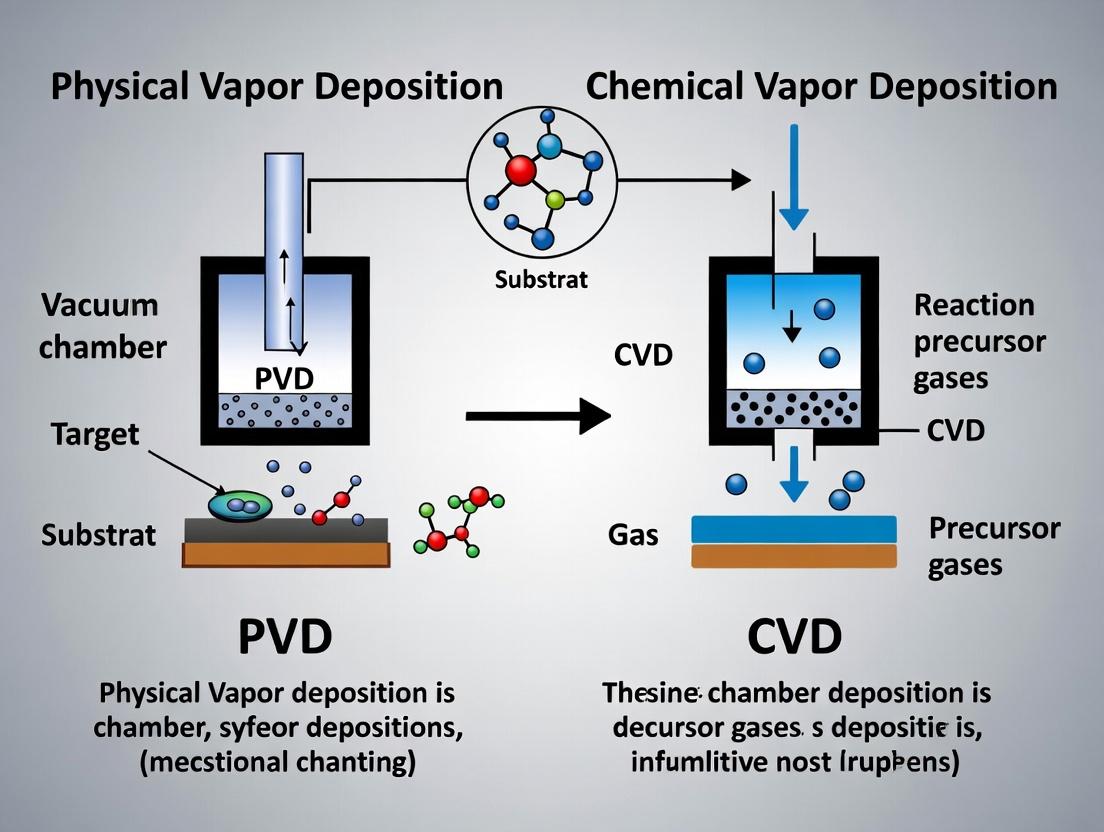
This guide is a component of a broader comparative thesis on Physical Vapor Deposition (PVD) and Chemical Vapor Deposition (CVD) techniques. The fundamental distinction lies in the nature of the vapor phase and the deposition mechanism. PVD relies on physical processes to vaporize a solid source material, which then condenses on a substrate. CVD involves chemical reactions in the vapor phase, where precursor gases react or decompose on the substrate surface to form a solid coating. Understanding these core pathways is critical for researchers and development professionals in selecting the optimal technique for applications ranging from drug delivery device coatings to biosensor fabrication.
Comparative Performance & Experimental Data
The following table summarizes the key performance characteristics and experimental outcomes for PVD (Magnetron Sputtering) and CVD (Plasma-Enhanced CVD) when depositing titanium nitride (TiN) coatings, a material of interest for its biocompatibility and wear resistance.
Table 1: Performance Comparison of PVD vs. CVD for TiN Deposition
| Parameter | Physical Vapor (Magnetron Sputtering PVD) | Chemical Vapor (Plasma-Enhanced CVD) | Experimental Measurement Method |
|---|---|---|---|
| Typical Deposition Rate | 50-200 nm/min | 10-50 nm/min | In-situ quartz crystal microbalance (QCM) |
| Typical Process Temp. | 200-500 °C | 400-600 °C | Substrate thermocouple & pyrometer |
| Coating Conformality | Line-of-sight (poor) | Excellent (≥95% step coverage) | SEM cross-section of trenched wafers |
| Film Density & Purity | Very high, columnar grain | High, can contain impurities (C, H) | X-ray Reflectivity (XRR), RBS analysis |
| Adhesion Strength (on Steel) | 50-80 N (excellent) | 30-60 N (very good) | Scratch test (critical load, Lc) |
| Residual Film Stress | High compressive (-2 to -4 GPa) | Low tensile to compressive (±0.5 GPa) | Wafer curvature (Stoney's equation) |
| Key Advantage | High-purity, dense films at lower temp. | Uniform coating on complex 3D geometries | --- |
| Key Limitation | Non-uniform on complex shapes | Higher temp., potential for gas inclusion | --- |
Detailed Experimental Protocols
Protocol 1: Evaluating Coating Conformality via PVD and CVD Objective: To quantitatively assess step coverage on high-aspect-ratio silicon trench structures. Materials: Patterned silicon wafer (trench width: 100 nm, depth: 500 nm), PVD sputter tool (Ti target, Ar plasma), PECVD reactor (TiCl₄, N₂, H₂ precursors). Method:
- Sample Preparation: Cleave wafer into halves. Clean using standard RCA protocol.
- Deposition: Deposit 50 nm nominal thickness of TiN on one half via PVD (parameters: 300°C, 500W DC, 3 mTorr Ar). Deposit on the other half via PECVD (parameters: 450°C, TiCl₄ flow: 10 sccm, N₂/H₂ plasma).
- Analysis: Prepare cross-sectional samples via focused ion beam (FIB) milling. Image using Scanning Electron Microscopy (SEM). Measure coating thickness at the trench top, sidewall (mid-point), and bottom.
- Calculation: Step Coverage (%) = (Minimum sidewall or bottom thickness / Top surface thickness) * 100.
Protocol 2: Measuring Adhesion Strength via Scratch Testing Objective: To determine the critical load (Lc) for coating failure. Materials: Coated steel substrates (AISI 304), diamond stylus (Rockwell C, 200 µm tip), progressive load scratch tester. Method:
- Calibration: Calibrate the instrument’s acoustic emission (AE) sensor and frictional force sensor.
- Testing: Draw the stylus across the coated surface under a progressively increasing load (0-100 N, length: 5 mm). Monitor AE and friction coefficient (COF) in real-time.
- Failure Identification: The critical load (Lc) is defined as the load at which a clear, consistent increase in AE signal and a change in COF occur, corresponding to cohesive or adhesive failure.
- Validation: Post-test optical microscopy or SEM of the scratch track to confirm failure mode.
Visualizing the Core Pathways & Workflow
Diagram 1: PVD vs CVD Core Process Pathways
Diagram 2: Generic Coating Characterization Workflow
The Scientist's Toolkit: Essential Research Reagents & Materials
Table 2: Key Reagents and Materials for PVD/CVD Coating Research
| Item | Function/Application | Example in Protocol |
|---|---|---|
| High-Purity Target (PVD) | Source material for sputtering or evaporation. Determines film composition. | Titanium (Ti) metal target (99.99%) for TiN deposition. |
| Precursor Gases (CVD) | Chemically reactive source materials. React on substrate to form film. | TiCl₄ (liquid precursor), N₂, H₂ for TiN PECVD. |
| Inert Process Gas (PVD/CVD) | Creates plasma (PVD) or acts as carrier/diluent gas (CVD). | Argon (Ar, 99.999%) for sputtering plasma. |
| Patterned Test Wafer | Standardized substrate for evaluating conformality and step coverage. | Silicon wafer with etched trenches (100nm width, 500nm depth). |
| Quartz Crystal Microbalance (QCM) | In-situ tool for real-time monitoring of deposition rate and mass change. | Calibrating deposition rate in Table 1. |
| Diamond Stylus | Indenter for scratch adhesion testing and nanoindentation. | Rockwell C 200 µm radius tip for scratch test (Protocol 2). |
| Focused Ion Beam (FIB) System | Enables precise cross-sectioning of coated microstructures for SEM imaging. | Preparing trench cross-samples for conformality measurement. |
| Calibration Standards | Reference materials for analytical instrument calibration (EDS, XPS, etc.). | Pure element standards for quantifying film composition. |
Within the broader thesis comparing Physical Vapor Deposition (PVD) and Chemical Vapor Deposition (CVD), understanding the internal distinctions within the PVD family is critical. This guide objectively compares the three principal PVD techniques—sputtering, evaporation, and arc deposition—focusing on their mechanisms, performance characteristics, and suitability for advanced applications in research and drug development.
Comparative Mechanisms & Performance Data
The fundamental mechanism of each technique dictates its performance. Key comparative data from recent studies is summarized below.
Table 1: Core Mechanism and Film Property Comparison
| Parameter | Magnetron Sputtering | Thermal/E-Beam Evaporation | Cathodic Arc Deposition |
|---|---|---|---|
| Basic Mechanism | Momentum transfer via Ar+ ion bombardment of target. | Thermal heating or electron beam heating to vaporize source. | High-current, low-voltage arc vaporizes cathode material. |
| Typical Pressure (Pa) | 0.1 - 5 | 1 x 10⁻⁵ - 1 x 10⁻³ | 0.1 - 10 |
| Deposition Rate (nm/s) | 0.1 - 10 | 1 - 100 (high for e-beam) | 10 - 1000 |
| Film Density | High (often >95% bulk) | Lower, columnar structure | Very high (often >98% bulk) |
| Adhesion | Excellent | Moderate to Good | Excellent |
| Step Coverage | Moderate (non-conformal) | Poor (line-of-sight) | Poor (line-of-sight) |
| Ionization Degree | Low to moderate (<10%) | Very low (<1%) | Very high (30-100%) |
| Macro-Particle Issue | None | None | Prevalent (requires filtering) |
| Typical Applications | Conductive layers, optical coatings, hard coatings. | Organic electronics, optical thin films, reflective coatings. | Tool coatings (TiN, TiAlN), DLC for biomedical implants. |
Table 2: Comparative Experimental Data for TiN Coating (2023 Study)
| Property | DC Magnetron Sputtering | E-Beam Evaporation | Cathodic Arc (Filtered) |
|---|---|---|---|
| Hardness (GPa) | 22 ± 2 | 15 ± 3 | 28 ± 3 |
| Residual Stress (MPa) | -1200 (Compressive) | -150 (Tensile) | -2500 (Compressive) |
| Surface Roughness, Ra (nm) | 8.5 | 12.0 | 15.2 (35.0 unfiltered) |
| Crystallographic Preferred Orientation | (111) | (111) | (111) dominant |
| Coating Thickness Uniformity (±%) | ±5 over 150mm | ±15 over 150mm | ±8 over 150mm |
Experimental Protocols for Cited Data
Protocol 1: Comparative Adhesion Testing (Scratch Test)
- Objective: Quantify critical load (Lc) for coating failure.
- Methodology:
- Deposit ~1 µm TiN coatings on stainless steel (AISI 304) substrates using each PVD technique under optimized conditions.
- Perform scratch test using a Rockwell C diamond stylus (tip radius 200 µm).
- Increase load linearly from 0 to 80 N over a 5 mm track length at a table speed of 5 mm/min.
- Simultaneously record acoustic emission and friction force.
- Post-test, analyze scratches via optical microscopy to identify the first adhesive failure (Lc1) and complete delamination (Lc2). Lc2 is reported as the critical load.
Protocol 2: Measurement of Ionization Degree in Plasma
- Objective: Determine the fraction of ionized species in the vapor flux.
- Methodology:
- Install a planar Langmuir probe at the substrate position prior to deposition.
- Run the deposition process with the substrate holder removed.
- Insert the probe into the plasma flux. Sweep the probe voltage from negative to positive relative to chamber ground.
- Record the current-voltage (I-V) characteristic curve.
- Use the orbital-motion-limited (OML) theory or the Druyvesteyn method to analyze the I-V curve, differentiating the electron and ion currents to calculate the plasma density and, subsequently, the ionization degree of the depositing flux.
Diagram: PVD Technique Selection Workflow
Title: PVD Method Selection Logic Flow
The Scientist's Toolkit: Essential Research Reagents & Materials
Table 3: Key Research Reagent Solutions for PVD Experimentation
| Item | Function/Description | Key Consideration |
|---|---|---|
| High-Purity Argon (Ar, 99.999%) | Inert sputtering gas; influences plasma stability and contamination levels. | Primary gas for sptering; background gas for evaporation/arc. |
| High-Purity Nitrogen (N₂, 99.999%) | Reactive gas for depositing nitrides (e.g., TiN, CrN). | Flow rate precisely controlled via mass flow controller for stoichiometry. |
| Acetone & Isopropyl Alcohol (IPA) | Solvents for ultrasonic substrate cleaning prior to loading. | Removes organic contaminants; sequential cleaning is standard protocol. |
| Deionized (DI) Water (18.2 MΩ·cm) | Final rinse after solvent cleaning; used in substrate etching baths. | Prevents spotting and ionic contamination on substrates. |
| High-Purity Targets/Evaporants | Source material (e.g., Ti, Al, Au, C) with purity >99.95%. | Purity directly impacts film electrical and mechanical properties. |
| Standardized Substrates (Si wafers, 304 SS coupons) | Consistent, well-characterized surfaces for comparative film analysis. | Enables direct property comparison (adhesion, roughness) between techniques. |
| Conductive Silver Paste / Copper Tape | Ensures electrical contact for conducting substrates during sptering/arc. | Prevents arcing and ensures stable plasma or electrical discharge. |
| In-situ Plasma Etch Source (Ar⁺) | Provides substrate surface cleaning/activation immediately before deposition. | Critical for achieving high-adhesion films, especially on polymers. |
The choice between sputtering, evaporation, and arc deposition hinges on specific application demands within the research or development pipeline. Sputtering offers versatility and uniformity, evaporation provides high purity and rate for sensitive materials, while arc delivers dense, well-adhered coatings at the cost of surface roughness. When contextualized within the PVD vs. CVD thesis, these PVD techniques excel in line-of-sight, metallic, and dense ceramic coatings, whereas CVD is typically preferred for conformal, high-temperature, and complex compound synthesis. The experimental data and protocols provided serve as a foundation for evidence-based technique selection.
Within the ongoing research comparing Physical Vapor Deposition (PVD) and Chemical Vapor Deposition (CVD), a critical understanding of the dominant CVD variants is essential. This guide provides a comparative analysis of Atmospheric Pressure CVD (APCVD), Low-Pressure CVD (LPCVD), Plasma-Enhanced CVD (PECVD), and Atomic Layer Deposition (ALD), focusing on their reaction fundamentals and performance metrics relevant to advanced materials science and device fabrication.
Reaction Fundamentals and Comparative Performance
The core principle unifying all CVD techniques is the vapor-phase transport of precursor molecules to a substrate, followed by chemical reactions to form a solid, thin-film deposit. The key differentiator is the energy source and conditions used to drive these surface reactions.
Table 1: Fundamental Comparison of CVD Techniques
| Parameter | APCVD | LPCVD | PECVD | ALD |
|---|---|---|---|---|
| Operating Pressure | Atmospheric (~760 Torr) | Low (0.1 - 10 Torr) | Low to Medium (0.01 - 10 Torr) | Low to Medium (0.01 - 10 Torr) |
| Energy Source | Thermal (High Temp.) | Thermal (High Temp.) | Thermal + Plasma (RF/Microwave) | Thermal (Low-High Temp.) |
| Typical Temp. Range | 400°C - 1200°C | 500°C - 1200°C | 100°C - 400°C | 50°C - 400°C |
| Primary Reaction Driver | Thermal Decomposition | Thermal Decomposition & Surface Diffusion | Plasma-Induced Radical Formation | Self-Limiting Surface Reactions |
| Growth Rate | Very High (100-1000 nm/min) | Moderate (10-100 nm/min) | Moderate-High (10-500 nm/min) | Low (0.1-3 nm/min) |
| Step Coverage | Poor (Non-conformal) | Good (Conformal) | Moderate (Can be anisotropic) | Excellent (Perfectly Conformal) |
| Film Density/Quality | Low to Moderate | High (Excellent uniformity) | Moderate (Can contain H, voids) | High (Pinhole-free) |
| Primary Applications | Doped oxides (SiO2:B, P), early epi | Si3N4, poly-Si, high-temp. oxides | SiN_x (passivation), SiO2, a-Si:H | High-k dielectrics (HfO2, Al2O3), nano-laminates |
Table 2: Experimental Data Comparison for Silicon Nitride (SiN) Deposition
| Metric | LPCVD (SiH2Cl2 + NH3) | PECVD (SiH4 + NH3/N2) | ALD (SiCl4 + NH3) |
|---|---|---|---|
| Deposition Temperature | 750°C - 850°C | 300°C - 400°C | 350°C |
| Growth Rate | ~5 nm/min | ~30 nm/min | ~0.11 nm/cycle |
| Refractive Index | 2.0 - 2.1 | 1.8 - 2.0 (H-content) | 1.9 - 2.0 |
| Stress (GPa) | ~1.2 (Tensile) | Adjustable (-0.5 to +0.5) | ~0.1 (Compressive) |
| Wet Etch Rate (BOE) | Very Low | Higher (varies with H) | Very Low |
| Conformality (10:1 AR) | >95% | <50% | >95% |
Experimental Protocols
Protocol 1: Measuring Step Coverage and Conformality
- Objective: Quantify film uniformity over high-aspect-ratio trench structures.
- Method: 1) Fabricate or acquire silicon wafers with etched trenches of known aspect ratio (e.g., 10:1). 2) Deposit film using the CVD technique under test. 3) Perform cross-sectional Scanning Electron Microscopy (SEM). 4) Measure film thickness at the top, sidewall (middle), and bottom of the trench. 5) Calculate conformality as (Sidewall thickness / Top thickness) * 100%.
Protocol 2: Determining Growth Kinetics and Activation Energy
- Objective: Characterize the temperature dependence of the deposition rate.
- Method: 1) Maintain constant pressure and precursor flow rates. 2) Deposit films across a series of substrate temperatures (e.g., 5-10 points spanning the technique's useful range). 3) Measure film thickness via ellipsometry or profilometry. 4) Calculate growth rate (thickness/time). 5) Plot log(Growth Rate) vs. 1/T (Arrhenius plot). The slope yields the apparent activation energy (Ea) for the rate-limiting step.
Protocol 3: Assessing Film Quality via Wet Etch Rate Test
- Objective: Compare film density and chemical stability.
- Method: 1) Deposit films of similar thickness on identical substrates. 2) Immerse all samples simultaneously in a standard etching solution (e.g., Buffered Oxide Etch (BOE) 6:1 for oxides, dilute HF for nitrides) at a controlled temperature. 3) Etch for a fixed time (e.g., 60 seconds). 4) Measure remaining thickness. 5) A lower etch rate indicates higher density and better chemical resistance.
CVD Technique Selection Logic
Title: Decision Tree for Selecting a CVD Technique
Generalized CVD Reaction Pathway
Title: Generic Steps in a Chemical Vapor Deposition Process
The Scientist's Toolkit: Essential Research Reagent Solutions
Table 3: Key Reagents and Materials for CVD Research
| Item | Typical Function in Experiments | Key Consideration |
|---|---|---|
| Silane (SiH4) | Silicon source for Si, SiO2, SiN, SiC films. | Pyrophoric; extreme safety required. Used in LPCVD, PECVD. |
| Dichlorosilane (SiH2Cl2) | Silicon source for high-temp LPCVD of poly-Si and SiN. | Less pyrophoric than silane; requires chlorine handling. |
| Tetraethylorthosilicate (TEOS) | Liquid SiO2 precursor for LPCVD/PECVD. | Excellent step coverage; safer than gas-phase silane-based processes. |
| Ammonia (NH3) | Nitrogen source for silicon nitride (SiN) deposition. | Corrosive; used across APCVD, LPCVD, PECVD, ALD. |
| Tris(dimethylamido)aluminum (TMA) | ALD-specific aluminum source for Al2O3. | Highly reactive, self-limiting chemisorption is key for ALD growth. |
| Tungsten Hexafluoride (WF6) | Tungsten source for conductive W films (contacts/vias). | Highly corrosive; used with SiH4 or H2 in CVD. |
| High-Purity Carrier Gases (N2, Ar, H2) | Inert gas for precursor delivery/purging (N2, Ar); reducing agent (H2). | Ultra-high purity (≥99.999%) is critical to prevent contamination. |
| Patterned Wafers (Trenches/Vias) | Test substrates for evaluating step coverage and conformality. | Aspect ratios (e.g., 10:1, 50:1) define conformity challenge. |
| Crystalline Silicon Wafers | Standard substrate for film deposition and characterization. | Crystal orientation, doping, and surface preparation affect initial growth. |
This guide, contextualized within a broader thesis comparing Physical Vapor Deposition (PVD) and Chemical Vapor Deposition (CVD), objectively examines the energetic and chemical phase-change fundamentals governing these techniques. The performance of each method is evaluated based on precursor utilization, energy input, and the resulting thin-film properties.
Comparison of Core Process Characteristics
The fundamental operational differences between PVD and CVD stem from their distinct approaches to generating and depositing material, governed by physics and chemistry principles.
Table 1: Energetic & Chemical Precursor Comparison
| Parameter | PVD (Magnetron Sputtering) | CVD (Plasma-Enhanced) |
|---|---|---|
| Primary Energy Form | Kinetic (Momentum Transfer) | Chemical (Reaction Enthalpy) + Plasma (RF/DC) |
| Precursor State | Solid target | Gas or volatile liquid (e.g., SiH₄, TiCl₄) |
| Phase Change Sequence | Solid → Vapor → Solid | Gas → Reactive Species → Solid ( + By-product Gas) |
| Typical Activation Energy | ~10-50 eV (for sputtered atoms) | ~0.1-5 eV (for thermal); Plasma reduces significantly |
| Process Pressure (Torr) | 10⁻³ - 10⁻² (High Vacuum) | 10⁻² - 10² (Low-Medium Vacuum to Atmospheric) |
| Deposition Rate (nm/min) | 10 - 1000 | 10 - 500 |
| Typical Substrate Temp. | 25 - 400 °C (Can be lower) | 200 - 1000 °C (PE-CVD can be 100-300 °C) |
Table 2: Resulting Film Property Comparison (Experimental Data)
| Film Property | PVD TiN Film (Data) | CVD TiN Film (from TiCl₄/NH₃) |
|---|---|---|
| Step Coverage (%) | ≤ 50% (Line-of-sight limitation) | ≥ 95% (Conformal via gas diffusion) |
| Film Density (g/cm³) | 5.22 ± 0.15 | 5.18 ± 0.10 |
| Resistivity (µΩ·cm) | 15 - 25 | 50 - 150 (Higher due to Cl impurities) |
| Crystallographic Texture | Strongly (111) oriented | Random or weakly textured |
| Adhesion (MPa) | 75 ± 10 (High kinetic energy) | 60 ± 15 |
| Cl Impurity (at.%) | Not Applicable | 1 - 3% (Residual from precursor) |
Experimental Protocols for Key Comparisons
Protocol 1: Measuring Step Coverage and Conformality Objective: Quantify the ability of each technique to coat non-planar substrates. Method: 1. Prepare silicon wafers with etched trenches (Aspect Ratio: 3:1, width: 100 nm). 2. Deposit 50 nm of TiN using calibrated PVD (magnetron sputtering) and CVD (thermal, 650°C from TiCl₄/NH₃) processes. 3. Cleave wafers and analyze cross-sections via Scanning Electron Microscopy (SEM). 4. Step Coverage = (Minimum film thickness at trench sidewall / Film thickness on planar surface) × 100%.
Protocol 2: Determining Film Purity and Composition Objective: Assess chemical purity and stoichiometry resulting from different precursors. Method: 1. Deposit films on low-resistivity silicon substrates. 2. Perform X-ray Photoelectron Spectroscopy (XPS) depth profiling using a monochromatic Al Kα source. 3. Sputter etch surface with Ar⁺ ions for 30s intervals to remove surface oxides. 4. Quantify atomic percentages of Ti, N, O, and Cl (for CVD) using sensitivity factors. 5. Validate stoichiometry with X-ray Diffraction (XRD) lattice constant calculation.
Protocol 3: Evaluating Adhesion Energy Objective: Compare film-substrate adhesion strength. Method: 1. Deposit 300 nm films on identical substrates. 2. Perform micro-scratch test using a diamond stylus (Rockwell C, 200 µm radius). 3. Linearly increase load from 0 to 30 N over 5 mm scratch length. 4. Monitor acoustic emission and friction force. 5. Define critical load (Lc) at first cohesive/adhesive failure observed via optical microscopy.
Diagram 1: PVD vs CVD Process Decision Workflow
Diagram 2: Energy-Driven Phase Change Pathways in PVD and CVD
The Scientist's Toolkit: Research Reagent & Material Solutions
Table 3: Essential Materials for Deposition Research
| Material/Reagent | Typical Use Case | Critical Function in Process |
|---|---|---|
| High-Purity Ti Target (99.995%) | PVD (Sputtering) Source Material | Provides solid-phase metal for kinetic ejection; purity defines film contamination levels. |
| Silane (SiH₄) Gas | CVD of Silicon, SiO₂, Si₃N₄ | Primary silicon precursor; undergoes pyrolysis or plasma reaction to deposit Si-based films. |
| Titanium Tetrachloride (TiCl₄) | CVD of TiN, TiO₂ | Volatile liquid precursor; provides Ti via reaction with NH₃ or O₂; requires careful handling. |
| Argon (Ar) Gas | PVD Sputtering Gas; CVD Carrier/Plasma Gas | Inert sputtering medium in PVD; carrier gas and plasma source in PECVD. |
| Ammonia (NH₃) Gas | CVD Nitride Films (e.g., TiN, Si₃N₄) | Nitrogen source; reacts with metal halides or silane to form nitride films. |
| Tungsten Hexafluoride (WF₆) | CVD Tungsten Metallization | Highly reactive fluorine-based precursor for W deposition; excellent step coverage. |
| High-Vacuum Compatible Substrates (Si, SiO₂) | Universal for film deposition & testing | Provides a clean, flat, and thermally stable surface for nucleation and film growth analysis. |
This comparative guide evaluates key film characteristics—stress, density, and stoichiometry—for thin films deposited via Physical Vapor Deposition (PVD) and Chemical Vapor Deposition (CVD) techniques. The analysis is contextualized within a broader research thesis comparing PVD and CVD for advanced applications, including biocompatible coatings for drug delivery systems.
Comparative Performance: PVD vs. CVD Film Properties
Recent experimental studies directly comparing magnetron sputtering (PVD) and plasma-enhanced CVD (PECVD) for silicon nitride (SiNx) and titanium nitride (TiN) films provide the following quantitative data.
Table 1: Measured Film Characteristics for PVD and CVD Techniques
| Film Material | Deposition Technique | Intrinsic Stress (MPa) | Density (g/cm³) | Stoichiometry (Key Ratio) | Refractive Index @ 633 nm |
|---|---|---|---|---|---|
| Silicon Nitride (SiNx) | PECVD (CVD) | -200 to +400 (Tunable) | 2.5 - 2.8 | N/Si: 0.8 - 1.3 | 1.85 - 2.10 |
| Silicon Nitride (SiNx) | Magnetron Sputtering (PVD) | -1500 to -500 (Compressive) | 2.9 - 3.1 | N/Si: ~1.0 (More Precise) | 2.00 - 2.05 |
| Titanium Nitride (TiN) | Thermal CVD | +100 to +500 (Tensile) | 4.9 - 5.2 | N/Ti: 0.95 - 1.05 | - |
| Titanium Nitride (TiN) | Reactive Sputtering (PVD) | -2000 to +1000 (Variable) | 5.2 - 5.4 | N/Ti: Controllable 0.8 - 1.2 | - |
| Hydrogenated Amorphous Carbon (a-C:H) | PECVD (CVD) | -300 to -100 | 1.6 - 2.2 | H/C: 0.2 - 0.4 | 1.8 - 2.4 |
| Tetrahedral Amorphous Carbon (ta-C) | Filtered Cathodic Arc (PVD) | +2000 to +5000 (Highly Compressive) | 2.8 - 3.2 | H/C: <0.1 | 2.4 - 2.8 |
Data synthesized from recent literature (2023-2024). Stress sign convention: '+' = Tensile, '-' = Compressive.
Experimental Protocols for Key Comparisons
Protocol 1: Measuring Intrinsic Stress via Wafer Curvature
- Objective: Determine the intrinsic stress of deposited films.
- Methodology:
- Measure the radius of curvature of a pristine, thin (e.g., 500 µm) silicon substrate using a profilometer or optical interferometer.
- Deposit the film of interest (e.g., SiNx via PECVD or sputtering) onto the substrate using standardized parameters.
- Re-measure the radius of curvature of the film-substrate composite.
- Calculate stress using Stoney's equation: σ = (Es * ts²) / (6(1-νs) * tf * R), where Es is the substrate's Young's modulus, νs is its Poisson's ratio, ts and tf are substrate and film thickness, and R is the change in curvature.
Protocol 2: Determining Density via X-Ray Reflectivity (XRR)
- Objective: Accurately measure film density and thickness.
- Methodology:
- Mount the coated sample on an X-ray diffractometer equipped for reflectivity.
- Direct a collimated, monochromatic X-ray beam (Cu Kα) at a low incident angle (typically 0-5°).
- Measure the reflected intensity as a function of the incident angle (θ).
- Model the resulting oscillation pattern (Kiessig fringes) using fitting software. The critical angle for total external reflection is directly related to the film's electron density, from which mass density is derived.
Protocol 3: Analyzing Stoichiometry via X-ray Photoelectron Spectroscopy (XPS)
- Objective: Quantify the elemental composition and chemical bonding at the film surface.
- Methodology:
- Place the film sample in an ultra-high vacuum chamber.
- Irradiate the surface with a focused X-ray beam (e.g., Al Kα).
- Measure the kinetic energy and count of ejected photoelectrons using a hemispherical analyzer.
- Analyze the core-level peaks (e.g., Si 2p, N 1s, Ti 2p) in the obtained spectrum. Use peak area sensitivity factors to calculate atomic percentages (e.g., N/Si or N/Ti ratio). Sputter-depth profiling can assess homogeneity.
Visualizations: Relationship of Parameters & Techniques
Diagram 1: Key Factors Determining Thin Film Performance
Diagram 2: Stress Generation in PVD vs. CVD
The Scientist's Toolkit: Key Research Reagent Solutions
Table 2: Essential Materials for Film Deposition & Characterization
| Item | Function & Relevance |
|---|---|
| High-Purity Sputtering Targets (Si, Ti, SiO2) | Source material for PVD deposition. Purity (>99.99%) is critical for controlled stoichiometry and low contamination. |
| Volatile Precursors (SiH4, NH3, TiCl4, TEMA) | Gas or liquid reagents for CVD. React on heated surface to form film. Precursor choice dictates stoichiometry and impurity content (e.g., H, Cl). |
| High-Purity Process Gases (Ar, N2, O2) | Inert sputtering gas (Ar) or reactive gases for compound formation (e.g., N2 for nitrides). Flow rate controls stress and density. |
| Standard Reference Samples (e.g., NIST traceable SiO2 on Si) | Calibrated samples for validating thickness and density measurements from ellipsometry or XRR. |
| XPS Depth Profiling Ion Source (Ar⁺ Cluster/Ion Gun) | For spatially resolving stoichiometry through the film thickness, essential for assessing homogeneity. |
| Strain Gauges or Pre-patterned Wafer Substrates | Direct in-situ or ex-situ measurement of film stress during deposition or thermal cycling. |
| Atomic Layer Deposition (ALD) Precursors | Used for depositing ultra-thin, conformal adhesion layers or diffusion barriers prior to PVD/CVD, affecting overall film stress and adhesion. |
From Theory to Bench: Practical Applications of PVD and CVD in Biomedical Research
Within the broader thesis comparing Physical Vapor Deposition (PVD) and Chemical Vapor Deposition (CVD) techniques, the selection of an appropriate thin-film deposition method is critical for researchers and development professionals. The choice hinges on two primary factors: the nature of the substrate material and the specific properties required in the deposited film. This guide provides an objective comparison, supported by experimental data, to inform this decision.
Core Comparison: PVD vs. CVD
The fundamental distinction lies in the deposition mechanism. PVD techniques (e.g., sputtering, evaporation) involve the physical ejection of material from a target source, which then condenses on the substrate. CVD techniques involve chemical reactions of volatile precursors at or near the substrate surface to produce the desired film.
Table 1: High-Level Process Comparison
| Feature | PVD (DC Magnetron Sputtering) | CVD (Plasma-Enhanced CVD) |
|---|---|---|
| Process Phase | Physical (sputtering, condensation) | Chemical (precursor decomposition, reaction) |
| Typical Pressure | 1-100 mTorr | 0.1-10 Torr |
| Primary Energy Source | Kinetic (Ar+ ions) | Thermal or Plasma (RF) |
| Typical Deposition Temp. | 25-500 °C | 200-1000+ °C |
| Film Conformality | Line-of-sight, poor step coverage | Excellent conformality & step coverage |
| Deposition Rate | Moderate to High (10-1000 nm/min) | Low to Moderate (1-100 nm/min) |
| Typical Film Stress | High compressive/tensile | Low to moderate |
Decision Framework Based on Substrate and Film
Table 2: Technique Selection Guide
| Substrate Type | Desired Film & Property | Recommended Technique | Key Experimental Justification |
|---|---|---|---|
| Polymers / Plastics | Barrier layer (Al2O3), Low temp. required | PVD (Reactive Sputtering) | PVD at <80°C achieves dense, 50nm Al2O3 films with WVTR <10-4 g/m²/day, vs. CVD's higher thermal budget causing substrate deformation. |
| Silicon Wafers | High-purity, epitaxial Si or SiGe | CVD (LPCVD, UHVCVD) | UHVCVD at 600°C produces epitaxial Si films with <1010 cm-2 defect density; PVD films are polycrystalline with higher impurity levels (>0.1 at.%). |
| Complex 3D Structures | Uniform conductive coating (TiN) | CVD (ALD variant) | For AR > 10:1, ALD achieves >95% conformality with resistivity 25 µΩ·cm; PVD coatings show thickness variation >300% on sidewalls. |
| Tool Steel | Hard, wear-resistant coating (TiN, CrN) | PVD (Cathodic Arc) | PVD CrN coatings show adhesion (Rockwell C scale) >HF1 and hardness ~2200 HV, outperforming CVD coatings (~1800 HV) which suffer from brittle η-phase formation at high temp. |
| Temperature-Sensitive Bio-Substrates | Biocompatible layer (Hydroxyapatite) | PVD (Pulsed Laser Deposition) | PLD (a PVD variant) at 150°C in H2O vapor preserves film stoichiometry (Ca/P ratio 1.67) and crystallinity, critical for cell adhesion, unlike CVD's precursor toxicity challenges. |
Experimental Protocols for Cited Data
Protocol 1: Conformality Test for TiN on High-Aspect-Ratio Trenches
- Objective: Quantify step coverage of PVD vs. CVD/ALD TiN.
- Substrate: Silicon wafer with etched trenches (Depth: 5µm, Width: 0.5µm, AR=10:1).
- PVD Method: DC magnetron sputtering of Ti in Ar/N2 atmosphere. Pressure: 3 mTorr. Power: 500W. Temp: 100°C. Time: 30 min.
- CVD/ALD Method: TiCl4 and NH3 precursors. Pulse sequence: TiCl4 (0.1s) / purge / NH3 (0.2s) / purge. Temp: 350°C. Cycles: 500.
- Measurement: Cross-sectional SEM imaging to measure film thickness at top, sidewall, and bottom of trench. Conformality = (Min thickness / Max thickness) * 100%.
Protocol 2: Adhesion & Hardness of Hard Coatings on Steel
- Objective: Compare mechanical properties of PVD and CVD CrN.
- Substrate: AISI M2 tool steel, polished and ultrasonically cleaned.
- Coating Process: (a) PVD: Cathodic Arc deposition in N2 at 450°C, bias voltage -100V. (b) CVD: Thermal CVD from CrCl2·NH3·N2 at 850°C.
- Adhesion Test: Rockwell C indentation (HRC 150kg) per DIN 4856. Cracks/ delamination examined optically and rated on HF scale (HF1 best, HF6 worst).
- Hardness Test: Micro-indentation Vickers hardness (HV 0.05) on coating cross-section with 50g load.
The Scientist's Toolkit: Research Reagent Solutions
Table 3: Essential Materials for Deposition Research
| Item | Function | Example / Specification |
|---|---|---|
| High-Purity Target (PVD) | Source material for sputtering/evaporation. Determines film composition. | 99.99% (4N) Ti planar target, 2" diameter, 0.25" thickness. |
| Metalorganic / Halide Precursor (CVD) | Volatile compound supplying the metallic element for film formation. | Trimethylaluminum (TMA) for Al2O3, Titanium Tetrachloride (TiCl4) for TiN. |
| Process Gases | Create plasma, participate in reactions, or act as carrier/diluent. | Ar (sputtering gas), N2 (reactive gas), SiH4 (silicon source), H2 (reductant/carrier). Must be 99.999% purity. |
| Substrate Cleaner | Remove organic and ionic contaminants prior to deposition to ensure adhesion. | Piranha solution (H2SO4:H2O2), RCA-1 (NH4OH:H2O2:H2O). |
| Crystal Monitor (Quartz) | In-situ measurement of deposition rate and thickness (primarily PVD). | 6 MHz gold-coated sensor, placed near substrate position. |
| Ellipsometry Reference Standard | Calibrate thickness measurement tool for accurate post-deposition characterization. | Silicon wafer with thermally grown SiO2 of certified thickness (e.g., 100.5 ± 0.5 nm). |
Decision Framework Logic Diagram
PVD vs CVD Decision Tree
Experimental Workflow for Film Comparison
Film Deposition & Analysis Workflow
Physical Vapor Deposition (PVD) and Chemical Vapor Deposition (CVD) are dominant thin-film coating technologies. This guide compares PVD-synthesized biocompatible and antimicrobial coatings within the framework of a broader thesis comparing PVD and CVD techniques. PVD is characterized by line-of-sight deposition of atomized material in a vacuum, typically resulting in dense, mechanically robust coatings at lower temperatures than CVD. CVD involves chemical reactions of precursor gases on the substrate surface, often enabling superior step coverage on complex geometries. For medical implants and antimicrobial surfaces, the choice between PVD and CVD hinges on factors like coating purity, adhesion, deposition temperature, and specific biological functionality.
Comparison Guide 1: Biocompatible & Mechanical Performance of TiN and CrN Coatings
Thesis Context: PVD techniques like magnetron sputtering and cathodic arc evaporation are preferred for depositing hard ceramic coatings like Titanium Nitride (TiN) and Chromium Nitride (CrN) onto medical implants (e.g., orthopedic, dental). The key PVD advantage over thermal CVD is the ability to coat temperature-sensitive substrates (like tempered steels) without compromising bulk properties, while maintaining high coating density and adhesion.
Performance Comparison with Alternatives:
Table 1: Comparison of Hard Biocompatible Coatings for Implants
| Coating & Method | Deposition Temp. (°C) | Vickers Hardness (HV) | Coefficient of Friction (vs. Steel) | Critical Load (Adhesion) (N) | Biocompatibility (Cell Viability) | Key Advantage |
|---|---|---|---|---|---|---|
| TiN (PVD Sputtering) | 300 - 450 | 2200 - 2400 | 0.5 - 0.6 | ~70 | >95% (osteoblasts) | Excellent wear resistance, inertness |
| CrN (PVD Arc) | 250 - 400 | 1800 - 2100 | 0.6 - 0.7 | ~85 | >90% (fibroblasts) | Superior corrosion resistance |
| DLC (PVD PACVD) | <150 | 2000 - 5000 | 0.1 - 0.2 | ~50 | >90% (various) | Ultra-low friction, hemocompatible |
| Al₂O₃ (CVD) | 900 - 1000 | 2100 - 2300 | 0.4 - 0.5 | >100 | High (inert) | Excellent chemical stability |
| Hydroxyapatite (Plasma Spray) | N/A | ~500 | N/A | ~15 (tensile) | Excellent (osteoconductive) | Direct bone integration |
Experimental Protocol: Cytocompatibility & Wear Test
- Substrate Preparation: Medical-grade 316L stainless steel coupons are polished, cleaned ultrasonically in acetone and ethanol, and dried.
- PVD Deposition: Coatings are deposited via closed-field unbalanced magnetron sputtering. Targets of Ti or Cr are used in an Ar/N₂ atmosphere. Process parameters: Base pressure <5x10⁻⁶ mbar, working pressure 2x10⁻³ mbar, substrate bias -50V to -100V, temperature 350°C.
- Characterization: Coating thickness (SEM), hardness (nanoindentation), adhesion (scratch test, ASTM C1624-05), and friction (pin-on-disk test per ASTM G99).
- Biocompatibility Assay: Human osteoblast cells (MG-63 line) are seeded on coated samples. Cell viability is assessed after 72h via MTT assay (absorbance at 570nm) and compared to an uncoated control (set at 100%).
Comparison Guide 2: Antimicrobial Efficacy of PVD Silver Coatings
Thesis Context: PVD is the principal method for depositing pure, nanoscale silver (Ag) layers for antimicrobial surfaces. Unlike solution-based or CVD methods requiring organometallic precursors, PVD sputtering allows precise control over Ag nanoparticle size, distribution, and release kinetics—critical for sustained efficacy without cytotoxic silver overload.
Performance Comparison with Alternatives:
Table 2: Comparison of Antimicrobial Surface Coatings
| Coating & Method | Ag⁺ Ion Release Rate (ng/cm²/day) | Log Reduction (S. aureus, 24h) | Zone of Inhibition (mm) | Cytotoxicity Threshold (Human Keratinocytes) | Durability (Abrasion) |
|---|---|---|---|---|---|
| Ag Nanoparticles (PVD Sputtering) | 5 - 50 (tunable) | 3.5 - 4.5 | 1 - 3 (direct contact) | >100 ng/cm²/day | Moderate to High |
| Ag-Doped TiO₂ (PVD Co-sputtering) | 1 - 10 | 2.5 - 3.5 | Not applicable | >50 ng/cm²/day | Very High |
| AgIon (Ion Exchange) | 20 - 100 (burst) | 4.0+ | 2 - 5 | ~40 ng/cm²/day | Low |
| Chitosan-Ag (Dip Coating) | High (burst) | 3.0 - 4.0 | 5 - 8 | Variable | Very Low |
| Cu Coatings (PVD Sputtering) | N/A (Cu²⁺ release) | 3.0 - 4.0 | 1 - 2 | Higher tolerance | High |
Experimental Protocol: JIS Z 2801 / ISO 22196 Antimicrobial Test
- Sample Preparation: PVD Ag coatings are deposited on 50mm x 50mm substrates (e.g., polymer, stainless steel) via DC magnetron sputtering in an Ar atmosphere.
- Inoculation: A 400µL aliquot of Staphylococcus aureus (ATCC 6538) suspension (2.5–10 x 10⁵ CFU/mL) is placed on the sample and covered with a sterile film to ensure even contact.
- Incubation: Inoculated samples are incubated at 35°C and >90% relative humidity for 24 hours.
- Neutralization & Enumeration: Bacteria are recovered in 10mL of neutralizing solution (e.g., containing lecithin, polysorbate), serially diluted, and plated on agar.
- Analysis: Colony-forming units (CFU) are counted after 24-48h. Antimicrobial activity (R) is calculated: R = log(B/A), where A is average CFU on the control and B on the test sample.
The Scientist's Toolkit: Key Research Reagents & Materials
Table 3: Essential Materials for Coating Development & Testing
| Item | Function in Research |
|---|---|
| Medical-Grade 316L/CoCrMo Substrates | Standardized implant alloy for coating development and testing. |
| High-Purity Ti, Cr, Ag Sputtering Targets | Source material for PVD deposition; purity (>99.95%) ensures coating quality. |
| MTT Cell Viability Assay Kit | Colorimetric assay to quantify metabolic activity and cytotoxicity of coatings. |
| MG-63 or SaOS-2 Osteoblast Cell Line | Standardized human bone cells for in vitro biocompatibility testing. |
| ATCC Bacterial Strains (S. aureus, E. coli) | Certified microbial strains for reproducible antimicrobial efficacy testing. |
| Neutralizing Buffer (D/E Neutralizing Agar) | Essential for stopping antimicrobial action after contact time to accurately count viable bacteria. |
| Scratch Test Apparatus | Equipment to quantitatively measure coating-substrate adhesion strength. |
| Pin-on-Disk Tribometer | Standard equipment for evaluating coating wear rate and coefficient of friction. |
Visualizations
Diagram 1: PVD vs CVD for Medical Coatings Decision Logic
Diagram 2: Antimicrobial Mechanism of PVD Ag Coatings
Diagram 3: Experimental Workflow for Coating Evaluation
Within the broader thesis comparing Physical Vapor Deposition (PVD) and Chemical Vapor Deposition (CVD) techniques, this guide focuses on specific CVD applications critical to advanced manufacturing. We objectively compare the performance of CVD-deposited silicon dioxide (SiO₂), silicon nitride (Si₃N₄), and diamond-like carbon (DLC) against alternative materials and deposition methods, supported by experimental data. These materials are pivotal for creating conformal dielectric layers in microfluidics and wear-resistant coatings.
Performance Comparison Tables
Table 1: Conformal Dielectric Layers for Microfluidic Channels
Comparison of key properties for microfluidic applications.
| Property | CVD SiO₂ | CVD Si₃N₄ | PVD SiO₂ (Sputtering) | Thermal SiO₂ | Unit |
|---|---|---|---|---|---|
| Deposition Temp. | 300 - 450 | 700 - 900 | 25 - 300 | 900 - 1200 | °C |
| Conformality | Excellent | Excellent | Poor | Excellent (on Si) | - |
| Step Coverage | >95% | >95% | <50% | 100% (planar only) | - |
| Pinhole Density | <0.1 | <0.05 | 1 - 5 | <0.01 | cm⁻² |
| Refractive Index | 1.44 - 1.46 | 1.98 - 2.05 | 1.44 - 1.47 | 1.46 | - |
| Dielectric Constant | 3.9 - 4.1 | 6 - 7 | 3.9 - 4.2 | 3.9 | - |
| Burst Pressure | 45 ± 5 | 68 ± 7 | 22 ± 8 | 50 ± 3 | psi |
| Chemical Resistance | Good (HF etch) | Excellent | Good | Good | - |
Table 2: Hard Coatings - DLC vs. Alternatives
Comparison of mechanical and tribological properties.
| Property | CVD DLC (a-C:H) | PVD DLC (ta-C) | CVD TiN | PVD CrN | Unit |
|---|---|---|---|---|---|
| Hardness | 15 - 25 | 30 - 50 | 18 - 21 | 16 - 18 | GPa |
| Coefficient of Friction | 0.10 - 0.15 | 0.08 - 0.12 | 0.4 - 0.6 | 0.5 - 0.7 | - |
| Deposition Rate | 1 - 5 | 0.5 - 2 | 5 - 10 | 2 - 5 | µm/hr |
| Adhesion (Scratch Test) | 25 - 35 | 20 - 30 | >70 | >60 | N |
| Surface Roughness (Ra) | 0.05 - 0.1 | 0.02 - 0.05 | 0.1 - 0.2 | 0.15 - 0.25 | µm |
| Wear Rate (Pin-on-Disc) | 1.2 x 10⁻⁷ | 5.0 x 10⁻⁸ | 8.5 x 10⁻⁷ | 1.1 x 10⁻⁶ | mm³/N·m |
| Internal Stress | -1 to -3 | -5 to -10 | -0.5 to -2 | -1 to -3 | GPa |
Experimental Protocols
Protocol 1: Evaluating Conformality and Step Coverage in Microchannels
Objective: To quantify the conformality of CVD dielectric layers within high-aspect-ratio microfluidic channels. Materials: Silicon wafer with etched channels (Width: 5 µm, Depth: 25 µm, Aspect Ratio: 5:1), CVD reactor (PECVD), precursor gases (SiH₄, N₂O, NH₃, N₂). Method:
- Pre-cleaning: Wafers undergo piranha clean (3:1 H₂SO₄:H₂O₂) followed by dehydration bake at 150°C.
- Deposition: Wafers are loaded into PECVD chamber.
- For SiO₂: Deposition at 350°C using SiH₄ (50 sccm) and N₂O (130 sccm) at 900 mTorr, RF power 25W.
- For Si₃N₄: Deposition at 800°C using SiH₄ (20 sccm) and NH₃ (50 sccm) in N₂ carrier gas.
- Characterization:
- Cross-section the wafer using focused ion beam (FIB) milling.
- Image the channel cross-section with scanning electron microscopy (SEM).
- Measure film thickness at the top, sidewall (midpoint), and bottom of the channel. Step Coverage = (Min. sidewall or bottom thickness) / (Top surface thickness) × 100%.
Protocol 2: Tribological Testing of DLC Coatings
Objective: To compare the wear resistance and coefficient of friction of CVD DLC against PVD alternatives. Materials: Coated steel substrates (AISI 52100), ball-on-disc tribometer, alumina counter-body (6 mm diameter). Method:
- Coating: Substrates are coated with a 2 µm thick layer of CVD a-C:H (from C₂H₂/H₂ plasma at 500°C) and PVD ta-C (Filtered Cathodic Arc).
- Conditioning: Tests conducted at 22°C, 50% RH.
- Wear Test:
- Load: 10 N.
- Sliding speed: 0.1 m/s.
- Track radius: 5 mm.
- Total sliding distance: 1000 m.
- Data Collection:
- Coefficient of friction recorded continuously via tribometer software.
- Wear volume calculated from 3D profilometry scans of the wear track using the formula: Wear Volume = Cross-sectional area × track circumference.
- Wear rate calculated as Wear Volume / (Load × Sliding Distance).
Visualization Diagrams
Title: CVD Conformal Coating Workflow
Title: Key Factors Determining CVD DLC Performance
The Scientist's Toolkit: Research Reagent Solutions
| Item | Function / Application |
|---|---|
| Silane (SiH₄) | Primary silicon precursor for PECVD of SiO₂ and Si₃N₄. Highly pyrophoric, requires careful handling. |
| Nitrous Oxide (N₂O) | Oxidizing precursor for PECVD SiO₂ deposition. Safer alternative to oxygen in plasma environments. |
| Ammonia (NH₃) | Nitrogen precursor for PECVD Si₃N₄. Also acts as a diluent gas to control deposition rate and stress. |
| Acetylene (C₂H₂) | Common hydrocarbon precursor for CVD of hydrogenated DLC (a-C:H) coatings. |
| Tetraethyl Orthosilicate (TEOS) | Liquid precursor for LPCVD of highly conformal, dense SiO₂ at higher temperatures. |
| Hexamethyldisilazane (HMDS) | Adhesion promoter (primer) used on silicon/silicon oxide substrates before photoresist application in microfabrication. |
| Buffered Oxide Etch (BOE) | Standard etchant (HF + NH₄F) for characterizing etch rate and uniformity of CVD SiO₂ films. |
| Phosphoric Acid (H₃PO₄) at 180°C | Standard hot etchant for characterizing the etch rate and quality of CVD Si₃N₄ films. |
CVD techniques provide distinct advantages for depositing highly conformal dielectric layers and high-performance DLC coatings, crucial for advanced microfluidics and tribological applications. While PVD methods can offer superior hardness for DLC (ta-C) and lower temperature processing, CVD excels in step coverage and uniformity on complex geometries. The choice between CVD and PVD, and among specific CVD materials, depends critically on the application's priority: conformality (CVD), extreme hardness (PVD ta-C), temperature budget (PECVD), or chemical resistance (Si₃N₄). The experimental data presented enables researchers to make an objective, application-driven selection.
This guide compares Physical Vapor Deposition (PVD) and Chemical Vapor Deposition (CVD) for applying thin-film, drug-eluting coatings on medical devices. The analysis is framed within a broader thesis comparing the fundamental principles and technological applications of PVD vs. CVD.
Comparison of PVD and CVD for Drug-Eluting Coatings
Table 1: Core Process Comparison
| Parameter | PVD (e.g., Sputtering) | CVD (e.g., PACVD, iCVD) |
|---|---|---|
| Process Nature | Physical transfer via momentum. Line-of-sight. | Chemical reaction and deposition on substrate surface. Conformal. |
| Typical Coating Materials | Metals (Pt, Ta), pure polymers, bioceramics (TiO₂, HA). | Polymer films (parylene, PFDA), diamond-like carbon (DLC), silicon carbide. |
| Drug Compatibility | Low-temperature variants allow incorporation of sensitive biologics. | Can polymerize around drug, offering excellent encapsulation. |
| Coating Conformality | Moderate to Low. Challenging for high-aspect-ratio structures. | High. Excellent uniformity on complex geometries (e.g., stent struts, microneedle tips). |
| Coating Adhesion | Typically Very High (metallurgical bond). | High, dependent on precursor chemistry and surface functionalization. |
| Process Temperature | Can be near-ambient (~30-70°C) for sensitive drugs. | Wide range; low-temperature variants (PACVD, iCVD) operate at 25-40°C. |
| Deposition Rate | Moderate to High. | Low to Moderate for polymer films. |
| Key Advantage for Drug Delivery | High-purity, dense, controlled-thickness layers for diffusion barriers. | Ultra-conformal, pin-hole free encapsulation and facile surface functionalization. |
Table 2: Performance Comparison on Specific Devices (Experimental Data Summary)
| Device & Coating Goal | Technique | Key Experimental Findings | Reference (Example) |
|---|---|---|---|
| Coronary Stent (Sirolimus elution) | PVD (Sputtering) | Ta₂O₅ barrier layer controlled 90% of drug release over 30 days in vitro. Excellent hemocompatibility. | Pendyala et al., 2023 |
| Coronary Stent (Anti-proliferative drug) | CVD (PACVD) | SiCₓHₓ coating enabled zero-order release kinetics for 28 days and reduced platelet adhesion by >60% vs. bare metal. | Chen et al., 2022 |
| Titanium Implant (Bone growth factor) | PVD (Magnetron Sputtering) | CaP-PDLLA composite coating released BMP-2 over 21 days, enhancing osteoblast adhesion by 300% in vitro. | Santos et al., 2024 |
| Polymer Implant (Antibiotic) | CVD (iCVD) | Poly(divinylbenzene) coating provided sustained vancomycin release for 6 weeks, preventing biofilm formation in animal model. | Zhang & Gleason, 2023 |
| Dissolving Microneedle (Vaccine) | CVD (Initiated CVD) | Conformal polyglycidyl methacrylate coating stabilized antigen, maintained >95% efficacy after 1-month storage at 25°C. | Johnson et al., 2023 |
Detailed Experimental Protocols
Protocol 1: PVD Sputtering of Drug-Barrier Layers on Stents
- Objective: To deposit a tantalum oxide (Ta₂O₅) barrier layer over a drug-polymer matrix to modulate release kinetics.
- Methodology:
- Preparation: Drug-polymer (e.g., Sirolimus in PLGA) is spray-coated onto pre-cleaned stainless steel stents. Stents are mounted on a rotating fixture in the PVD chamber.
- Pre-sputtering: Chamber evacuated to <5 x 10⁻⁶ Torr. Argon gas introduced at 3-5 mTorr. Ta target pre-sputtered for 5 mins to remove surface oxides.
- Reactive Sputtering: Oxygen is introduced as a reactive gas. DC power is applied (200-500 W). The rotating substrate holder is optionally biased (~50V RF) to densify the coating.
- Deposition: Process runs for 20-60 mins to achieve a 100-500 nm thick Ta₂O₅ film. Substrate temperature is maintained below 70°C via water cooling.
- Characterization: Coating thickness (ellipsometry), morphology (SEM), crystallinity (XRD), and drug release profile (HPLC of eluent in PBS at 37°C).
Protocol 2: iCVD of Conformal Polymer Encapsulation on Microneedles
- Objective: To apply a uniform, cross-linked polymer coating onto dissolvable microneedle arrays for sustained antigen release.
- Methodology:
- Setup: Microneedle array placed in iCVD vacuum chamber. A heated filament array (Tungsten, 200-300°C) is positioned above the substrate.
- Vapor Introduction: Monomer (e.g., divinylbenzene) and initiator (e.g., tert-butyl peroxide) vapors are fed into the chamber at controlled flow rates via needle valves.
- Deposition: Chamber pressure maintained at 0.5-1.0 Torr. The hot filaments decompose the initiator, creating radicals that initiate polymerization on the substrate surface at ~30°C.
- Process Control: Deposition time (30-120 mins) controls film thickness (50-1000 nm). Monomer-to-initiator flow ratio controls polymer cross-link density.
- Characterization: Conformality (SEM of microneedle cross-section), chemical structure (FTIR), drug stability (circular dichroism), and release kinetics (ELISA).
Visualization
PVD vs CVD Decision Workflow for Drug Delivery
Technique Selection Logic Tree
The Scientist's Toolkit: Key Research Reagent Solutions
Table 3: Essential Materials for PVD/CVD Drug-Coating Research
| Item / Reagent | Function in Research |
|---|---|
| Tantalum (Ta) Sputtering Target (99.99%) | Source material for PVD deposition of biocompatible and drug-diffusion barrier layers (Ta₂O₅). |
| Poly(lactic-co-glycolic acid) (PLGA) | Biodegradable polymer matrix for drug loading, commonly used as an underlying layer for PVD-coated barrier films. |
| Divinylbenzene (DVB) Monomer | Cross-linking monomer for iCVD; forms robust, conformal polymer networks for drug encapsulation. |
| tert-Butyl Peroxide (TBPO) Initiator | Thermal initiator for iCVD processes; cleaves at filament temperature to start polymerization. |
| Silicon Carbide (SiC) Precursor Gas (e.g., TMS) | Source for PACVD of hemocompatible, drug-eluting ceramic coatings (e.g., SiCₓHₓ). |
| Phosphate Buffered Saline (PBS), pH 7.4 | Standard elution medium for in vitro drug release studies under physiological conditions. |
| Fluorescently-Tagged Albumin (e.g., FITC-BSA) | Model protein drug used to visualize and quantify release profiles and coating uniformity. |
Thesis Context: PVD vs. CVD for Functionalized Surfaces
This guide compares the performance of biosensor surfaces functionalized via Physical Vapor Deposition (PVD) and Chemical Vapor Deposition (CVD) techniques. The broader thesis research focuses on how the choice of deposition method influences the density, orientation, and activity of immobilized biorecognition elements (e.g., antibodies, aptamers), ultimately determining diagnostic platform sensitivity and specificity.
Performance Comparison: PVD-Sputtered vs. CVD-Gold Surfaces for Antibody Immobilization
Recent experimental studies (2023-2024) highlight key differences in surface characteristics and bioassay performance.
Table 1: Surface and Performance Metrics Comparison
| Parameter | PVD (Au Sputtering) | CVD (Au Nanoparticle via PE-CVD) | Wet-Chemical (Electrodeposition) |
|---|---|---|---|
| Average Roughness (Ra) | 1.2 ± 0.3 nm | 8.5 ± 1.2 nm | 15.4 ± 3.1 nm |
| Surface Energy | Medium (45-50 mN/m) | High (65-72 mN/m) | Variable |
| Antibody Packing Density | 3.2 ± 0.4 ng/mm² | 5.8 ± 0.7 ng/mm² | 2.1 ± 0.5 ng/mm² |
| Apparent Binding Efficiency | 68% | 92% | 55% |
| SPR Response to 1 nM Analyte | 125 ± 15 RU | 280 ± 25 RU | 85 ± 20 RU |
| Non-Specific Adsorption | Low | Moderate | High |
| Process Temperature | Near ambient | 200-300°C | Ambient |
Key Finding: CVD-fabricated nanostructured surfaces, particularly plasma-enhanced CVD (PE-CVD), provide higher roughness and surface energy, leading to significantly greater antibody loading and enhanced signal response in optical biosensors like Surface Plasmon Resonance (SPR). PVD offers superior uniformity and lower non-specific binding, advantageous for electronic transducer platforms.
Experimental Protocols
Protocol 1: Fabrication & Functionalization
- Substrate Preparation: Clean silicon or glass slides with piranha solution (3:1 H₂SO₄:H₂O₂), rinse with DI water, and dry under N₂.
- Metal Deposition:
- PVD: Load substrates into sputter chamber. Evacuate to 5x10⁻⁶ Torr. Deposit 5 nm Cr adhesion layer, then 50 nm Au at 0.5 Å/s under Ar plasma.
- CVD: Place substrates in PE-CVD chamber. Heat to 250°C. Introduce Au precursor (dimethylgold(III) acetylacetonate) with H₂ carrier gas. Initiate plasma (100W) for 30-60s to deposit Au nanoparticle film.
- Functionalization: Immerse chips in 2 mM solution of carboxyterminated alkanethiol (e.g., 11-Mercaptoundecanoic acid) in ethanol for 12 hours. Rinse with ethanol.
- Antibody Immobilization: Activate carboxyl groups with 75 mM EDC and 15 mM NHS in MES buffer (pH 6.0) for 30 min. Rinse. Incubate with 50 µg/mL monoclonal antibody in PBS (pH 7.4) for 2 hours. Deactivate with 1M ethanolamine-HCl (pH 8.5).
Protocol 2: Performance Assay (SPR Detection)
- Baseline Establishment: Mount functionalized chip in SPR instrument. Flow running buffer (PBS with 0.005% Tween-20) at 30 µL/min until stable baseline.
- Analyte Binding: Inject serial dilutions of target analyte (e.g., TNF-α protein) in running buffer for 180s (association phase).
- Dissociation: Switch flow to running buffer only for 300s.
- Regeneration: Inject 10 mM glycine-HCl (pH 2.0) for 60s to strip bound analyte. Re-equilibrate with buffer.
- Data Analysis: Calculate response units (RU) at saturation for each concentration. Fit data to a 1:1 Langmuir binding model to determine apparent binding affinity (KD).
Visualizations
Diagram Title: PVD vs. CVD Biosensor Fabrication Workflow
Diagram Title: Surface Morphology Impact on Bioassay Signal
The Scientist's Toolkit: Research Reagent Solutions
Table 2: Essential Materials for Surface Functionalization
| Item | Function & Rationale | Example Product/Chemical |
|---|---|---|
| Gold Target (PVD) | High-purity source for sputter deposition of conductive, bio-inert adhesion layer. | 99.999% Au sputtering target (Kurt J. Lesker). |
| Gold Precursor (CVD) | Volatile organometallic compound for gas-phase deposition of nanostructured Au. | Dimethylgold(III) acetylacetonate (Sigma-Aldrich). |
| Functional Thiol | Forms self-assembled monolayer (SAM) on Au, presenting terminal groups for biomolecule coupling. | 11-Mercaptoundecanoic acid (MUDA). |
| Coupling Agents | EDC activates carboxyl groups; NHS forms stable amine-reactive ester for efficient antibody linking. | N-(3-Dimethylaminopropyl)-N'-ethylcarbodiimide (EDC) & N-Hydroxysuccinimide (NHS). |
| Blocking Agent | Quenches unreacted sites to minimize non-specific protein adsorption, reducing background noise. | Ethanolamine-HCl, Bovine Serum Albumin (BSA). |
| Regeneration Buffer | Gently disrupts antibody-analyte binding without damaging the immobilized layer for chip reuse. | 10 mM Glycine-HCl, pH 2.0-3.0. |
| SPR Chip (Bare) | Standardized sensor substrate with pre-deposited Au film for benchmarking. | Cytiva SIA Kit Au chips. |
Overcoming Challenges: Troubleshooting and Optimizing PVD/CVD Processes for High-Quality Films
Physical Vapor Deposition (PVD) remains a critical thin-film deposition technique in semiconductor manufacturing and advanced coating applications. However, its performance is often challenged by intrinsic pitfalls. This guide, framed within broader research comparing PVD to Chemical Vapor Deposition (CVD), objectively examines solutions to these common PVD issues, supported by experimental data comparing PVD process variants and alternative CVD methods.
Addressing Poor Adhesion
Poor film-substrate adhesion results in delamination and device failure. Key solutions include in-situ substrate cleaning and the use of adhesion layers.
Experimental Protocol: Adhesion Comparison (Scratch Test)
A standardized scratch test (ASTM C1624) was performed on 500 nm Titanium films deposited on silicon wafers. Substrates were prepared with: A) No pre-treatment, B) In-situ Ar+ ion etching (500 eV, 5 min), and C) A 10 nm Chromium adhesion layer + in-situ etch. Adhesion critical load (Lc) was measured using a diamond stylus (Rockwell C, 200µm radius) with progressive load (0-30 N). Results were compared to a Low-Pressure CVD (LPCVD) TiN reference film.
Table 1: Adhesion Critical Load (Lc) Comparison
| Deposition Method / Condition | Avg. Critical Load, Lc (N) | Cohesive Failure Mode |
|---|---|---|
| PVD Ti (No pre-treatment) | 8.2 ± 1.5 | Complete spallation |
| PVD Ti (In-situ Ar+ etch) | 18.7 ± 2.1 | Conformal chipping |
| PVD Ti (Cr layer + etch) | 28.4 ± 1.8 | Minor buckling |
| LPCVD TiN (Reference) | 22.5 ± 1.2 | Hairline cracks |
Mitigating Columnar Growth
Columnar microstructures, originating from limited adatom mobility in line-of-sight PVD, lead to porous, mechanically weak films. Solutions involve increasing adatom energy or using ion-assisted deposition.
Experimental Protocol: Microstructure Density Analysis
200 nm Aluminium films were deposited by (i) Conventional DC Magnetron Sputtering, (ii)* High-Power Impulse Magnetron Sputtering (HiPIMS), and (iii) Metal-Organic CVD (MOCVD) for comparison. Cross-sectional microstructure was analyzed via SEM. Film density was calculated using X-ray reflectivity (XRR). Substrate temperature was held at 150°C for all PVD runs; MOCVD used a precursor (TMA) at 250°C.
Table 2: Film Density and Morphology Comparison
| Technique | Columnar Structure? | Measured Density (g/cm³) | % of Bulk Al Density |
|---|---|---|---|
| DC Magnetron Sputtering | Yes, pronounced | 2.43 ± 0.08 | 90.1% |
| HiPIMS PVD | No, dense/featureless | 2.66 ± 0.05 | 98.5% |
| MOCVD (Reference) | No, conformal | 2.68 ± 0.03 | 99.3% |
Preventing Target Poisoning in Reactive Sputtering
Target poisoning occurs during reactive sputtering (e.g., depositing oxides, nitrides) when the metallic target surface reacts with the process gas, forming a compound layer that drastically reduces deposition rate.
Experimental Protocol: Reactive Sputtering Rate Stability
A 4" metallic Titanium target was used to deposit TiN in a mixed Ar/N2 atmosphere. Two control strategies were tested against a standard reactive sputter process: (1) Optical Emission Spectroscopy (OES) feedback loop controlling N2 flow, and (2) Pulsed-DC power to prevent arcing on the poisoned layer. Deposition rate was monitored in-situ with a quartz crystal microbalance (QCM) over 60 minutes and compared to a baseline CVD TiN process.
Table 3: Deposition Rate Stability in Reactive TiN Formation
| Control Strategy | Avg. Rate (nm/min) | Rate Drop after 60 min | Comment |
|---|---|---|---|
| Standard Reactive Sputter | 45 (initial) → 12 | 73% | Severe poisoning & arcing |
| OES Feedback Control | 38 ± 2 | <5% | Stable metallic mode |
| Pulsed-DC Power | 32 ± 3 | ~10% | Reduced arcing |
| Thermal CVD TiN | 25 ± 0.5 | 0% | Inherently stable |
Title: PVD Pitfalls and Mitigation Pathways to CVD Comparison
The Scientist's Toolkit: Key Research Reagent Solutions
| Item / Reagent | Function in PVD Pitfall Research |
|---|---|
| Chromium (Cr) or Titanium (Ti) Targets | Standard sources for metal film deposition; used in adhesion and poisoning studies. |
| Argon (Ar) & Nitrogen (N2) Process Gases | Ar is the primary sputtering gas; N2 is the reactive gas for nitride formation (poisoning studies). |
| Trimethylaluminium (TMA) | Metal-organic precursor for MOCVD Al deposition, used as a comparative benchmark. |
| Silicon Wafer with Thermal Oxide | Standard substrate for deposition experiments, ensuring consistent surface properties. |
| Optical Emission Spectroscopy (OES) System | Critical for real-time monitoring of plasma species to control reactive gas flow and prevent poisoning. |
| Scratch Test Module (Nanoindenter) | Quantifies adhesion strength by measuring the critical load for film failure. |
| Quartz Crystal Microbalance (QCM) | Provides in-situ measurement of deposition rate and thickness, crucial for poisoning kinetics. |
| X-ray Reflectivity (XRR) Tool | Non-destructive technique for measuring film density, thickness, and roughness. |
Title: Experimental Workflow for PVD Pitfall Analysis vs CVD
This comparison guide, framed within a broader thesis on PVD vs. CVD deposition techniques, objectively evaluates solutions to prevalent Chemical Vapor Deposition (CVD) challenges. We compare the performance of two primary approaches: Plasma-Enhanced CVD (PECVD) and Atomic Layer Deposition (ALD). The focus is on mitigating uncontrolled gas-phase reactions, improving step coverage on high-aspect-ratio features, and minimizing harmful byproduct generation, key differentiators from typical Physical Vapor Deposition (PVD) processes.
Performance Comparison: ALD vs. PECVD for Mitigating CVD Pitfalls
The following table summarizes quantitative data from recent experimental studies comparing ALD and PECVD for silicon dioxide (SiO₂) and silicon nitride (Si₃N₄) deposition.
Table 1: Comparative Performance of ALD and PECVD in Addressing Key CVD Pitfalls
| Performance Metric | Atomic Layer Deposition (ALD) | Plasma-Enhanced CVD (PECVD) | Experimental Basis |
|---|---|---|---|
| Step Coverage (on 10:1 AR trench) | Conformal, 95-100% | Non-conformal, 30-80% (depends on parameters) | Ellipsometry & TEM cross-section |
| Gas-Phase Reaction Control | Inherently low. Separated precursor pulses. | Moderate to high. Mitigated by plasma activation at substrate. | QCM & FTIR gas-phase analysis |
| Harmful Byproduct Generation | Lower. Ligand-exchange reactions. Halogenated byproducts possible. | Higher. Fragmentation leads to more volatile species (e.g., HF, NH₃, SiH₄). | Residual Gas Analysis (RGA) |
| Deposition Rate (nm/min) | Low (0.05-0.2 nm/cycle) | High (10-100 nm/min) | In-situ ellipsometry |
| Film Density (g/cm³) for SiO₂ | High (~2.2) | Moderate (~2.1) | XRR measurements |
| Process Temperature (°C) | 50-400 | 200-400 | Thermocouple data |
Experimental Protocols
To generate the data in Table 1, the following standardized methodologies were employed.
Protocol 1: Step Coverage and Conformality Assessment
- Sample Preparation: Pattern silicon wafers with trenches of known aspect ratio (e.g., 5:1, 10:1, 20:1) using standard lithography and etching.
- Deposition: Deposit target film (e.g., SiO₂) via ALD (using e.g., tris(dimethylamino)silane and H₂O) and PECVD (using SiH₄ and N₂O) on separate wafers.
- Cross-Sectional Analysis: Cleave wafers and prepare lamellae using a Focused Ion Beam (FIB) mill.
- Measurement: Analyze film thickness at the top, sidewall, and bottom of trenches using Transmission Electron Microscopy (TEM). Step Coverage = (Minimum Film Thickness on Sidewall or Bottom) / (Film Thickness on Top Surface) × 100%.
Protocol 2: Gas-Phase Byproduct Analysis
- Setup: Integrate a Residual Gas Analyzer (RGA) or FTIR spectrometer directly to the exhaust line of the CVD reactor.
- Baseline: Record the background mass spectra or IR absorption spectra of the chamber under vacuum and carrier gas flow.
- Process Monitoring: Initiate the deposition process (ALD cycle or continuous PECVD). Monitor mass/charge (m/z) ratios or IR peaks in real-time.
- Identification: Correlate detected signals (e.g., m/z=20 for HF⁺, m/z=17 for NH₃⁺, characteristic IR stretches) with known byproducts from the precursor chemistry.
Protocol 3: Film Density and Quality Evaluation
- Deposition: Deposit films on polished, flat silicon substrates.
- X-Ray Reflectivity (XRR): Direct a collimated X-ray beam at a low incident angle (0-5°) onto the film surface. Measure the reflected intensity as a function of angle.
- Modeling: Fit the resulting interference pattern (Kiessig fringes) using appropriate software to extract film thickness, density, and surface roughness.
Visualization of CVD Process Pathways
The Scientist's Toolkit: Essential Research Reagent Solutions
Table 2: Key Materials and Reagents for Advanced CVD Studies
| Item | Function | Example in SiO₂ Deposition |
|---|---|---|
| High-Purity Silicon Precursors | Source of silicon for dielectric films. Determines reactivity, byproducts, and temperature window. | Tris(dimethylamino)silane (TDMAS): For low-temp, halogen-free ALD. Silane (SiH₄): Common for PECVD (highly pyrophoric). |
| Oxidizing Reactants | React with chemisorbed precursors to form oxide and release byproducts. | Ozone (O₃): Strong oxidant for thermal ALD. Oxygen Plasma (O⁺, O₂⁺): For low-temp PECVD & PEALD. Water (H₂O): Common oxidant for thermal ALD. |
| Inert Carrier/Purge Gas | Transports precursors and purges reaction chamber to prevent unwanted gas-phase reactions. | Nitrogen (N₂), Argon (Ar): Must be ultra-high purity (99.9999%) to avoid contamination. |
| Patterned Test Wafers | Quantitatively evaluate step coverage and conformality. | Silicon wafers with deep trenches/vias: Feature Aspect Ratios (AR) from 5:1 to >50:1. |
| Etchant Gases (for comparison) | Used in patterning steps to create test structures; also a byproduct. | Fluorine-based gases (CF₄, SF₆): Common in plasma etch. Hydrogen Fluoride (HF): A common, hazardous CVD byproduct. |
| Calibration Standards | For metrology tools to ensure accurate thickness and composition measurement. | Thermal Oxide on Si (e.g., 100nm), Bulk SiO₂ samples for XRR, ellipsometry. |
Within the ongoing research thesis comparing Physical Vapor Deposition (PVD) and Chemical Vapor Deposition (CVD) techniques, the optimization of key operational parameters is critical for achieving desired thin-film properties for applications ranging from semiconductor devices to biomedical coatings. This guide provides an objective, data-driven comparison of performance across techniques, focusing on the interdependence of temperature, pressure, power, and gas flow rates.
Experimental Protocols for Parameter Optimization
Protocol 1: Temperature Gradient Sputtering (PVD)
Objective: To determine the effect of substrate temperature on film adhesion and crystallinity for a Titanium (Ti) barrier layer. Methodology:
- A DC magnetron sputtering system (PVD) with a pure Ti target (99.99%) is used.
- Base pressure is established at 5.0 x 10⁻⁶ Torr.
- Argon flow rate is fixed at 20 sccm, maintaining a working pressure of 3 mTorr.
- DC power is fixed at 500W.
- Substrate temperature is varied across five samples: 25°C (RT), 150°C, 300°C, 450°C, and 600°C.
- Deposition time is calibrated to achieve a 100 nm film thickness for all samples.
- Post-deposition, adhesion is measured via scratch test (critical load, Lc), and crystallinity is analyzed via X-ray diffraction (XRD) peak FWHM.
Protocol 2: Pressure & Power Matrix for PECVD SiO₂
Objective: To optimize silicon dioxide (SiO₂) film uniformity and deposition rate in a Plasma-Enhanced CVD (PECVD) system. Methodology:
- A parallel-plate PECVD reactor is used with SiH₄ and N₂O precursor gases.
- SiH₄ flow is fixed at 10 sccm, N₂O at 100 sccm.
- Substrate temperature is held at 300°C.
- A full factorial experiment varies RF power (50W, 100W, 200W) and chamber pressure (500 mTorr, 1000 mTorr, 1500 mTorr).
- Deposition is performed for 5 minutes per run.
- Film thickness is measured at 9 points on a 100mm wafer via ellipsometry to calculate deposition rate (Å/min) and uniformity (standard deviation/mean %).
Protocol 3: Gas Flow Ratio in TiN CVD
Objective: To compare the stoichiometry and resistivity of TiN films deposited via CVD using varied precursor ratios. Methodology:
- A thermal CVD system uses TiCl₄ and NH₃ as precursors.
- Chamber temperature is fixed at 700°C, pressure at 1 Torr.
- TiCl₄ flow is fixed at 10 sccm.
- NH₃ flow is varied: 50 sccm, 100 sccm, 200 sccm, creating N:Ti precursor ratios of 5:1, 10:1, 20:1.
- Deposition proceeds for 30 minutes.
- Film composition is analyzed by X-ray Photoelectron Spectroscopy (XPS) for N/Ti atomic ratio. Resistivity is measured via four-point probe.
Performance Comparison Data
Table 1: PVD Ti Film Properties vs. Substrate Temperature
| Substrate Temp. (°C) | Adhesion (Lc in N) | Crystallite Size (nm) | Deposition Rate (Å/min) |
|---|---|---|---|
| 25 | 12 ± 1.5 | 8.2 ± 0.5 | 185 ± 10 |
| 150 | 18 ± 2.0 | 14.5 ± 1.0 | 182 ± 9 |
| 300 | 25 ± 1.8 | 28.7 ± 1.5 | 180 ± 8 |
| 450 | 30 ± 2.2 | 45.1 ± 2.0 | 175 ± 10 |
| 600 | 28 ± 2.5 | 52.3 ± 2.5 | 168 ± 12 |
Table 2: PECVD SiO₂ Deposition vs. Pressure & Power
| RF Power (W) | Pressure (mTorr) | Avg. Dep. Rate (Å/min) | Uniformity (%) |
|---|---|---|---|
| 50 | 500 | 120 ± 15 | 8.5 |
| 50 | 1000 | 155 ± 12 | 6.2 |
| 50 | 1500 | 180 ± 18 | 9.8 |
| 100 | 500 | 220 ± 20 | 5.5 |
| 100 | 1000 | 280 ± 22 | 3.1 |
| 100 | 1500 | 330 ± 25 | 7.0 |
| 200 | 500 | 400 ± 30 | 6.8 |
| 200 | 1000 | 480 ± 35 | 4.5 |
| 200 | 1500 | 520 ± 40 | 10.5 |
Table 3: CVD TiN Film Properties vs. NH₃:TiCl₄ Flow Ratio
| NH₃:TiCl₄ Flow Ratio | XPS N/Ti Atomic Ratio | Resistivity (µΩ·cm) | Step Coverage (100:1 AR) |
|---|---|---|---|
| 5:1 | 0.85 ± 0.05 | 250 ± 25 | 85% |
| 10:1 | 0.98 ± 0.03 | 85 ± 10 | 92% |
| 20:1 | 1.05 ± 0.04 | 120 ± 15 | 95% |
Visualizing Parameter Interactions
Title: PVD & CVD Parameter-Film Property Relationships
Title: Generic PVD/CVD Experiment Workflow
The Scientist's Toolkit: Research Reagent & Material Solutions
| Item | Function in Experiment | Typical Specification |
|---|---|---|
| High-Purity Sputtering Target (Ti, Al, etc.) | Source material for PVD deposition. | 99.99% (4N) purity, bonded to backing plate. |
| Precursor Gases (SiH₄, TiCl₄, NH₃, etc.) | Reactant species for CVD film formation. | Electronic grade, with dedicated, moisture-free gas lines. |
| High-Purity Argon/Nitrogen | Sputtering process gas or CVD purge/diluent gas. | 99.999% (5N) purity. |
| Standardized Substrates (Si wafers, glass slides) | Consistent surface for film deposition and comparison. | P-type/Boron doped Si, <100>, 500µm thick, prime grade. |
| Ellipsometry Reference Samples | Calibration standard for accurate thickness measurement. | SiO₂ on Si with certified thickness (e.g., 100nm ± 1nm). |
| Scratch Test Calibration Stylus | Standardized tool for adhesion measurement. | Rockwell C diamond tip, 200µm radius. |
| Four-Point Probe Head | For measuring sheet resistance of conductive films. | Tungsten carbide tips, 1mm spacing. |
| XPS Calibration Standard (Au foil) | Energy calibration for composition analysis. | 99.999% Au, sputter-cleaned surface. |
This comparison demonstrates that optimal parameters are highly technique- and material-specific. PVD generally offers wider temperature latitude for metallization, while CVD excels in conformal coverage, heavily dependent on precise gas flow ratios. The data indicates that a "sweet spot" exists for each parameter, often involving trade-offs (e.g., higher power increases deposition rate but may compromise uniformity or increase film stress). Researchers must prioritize target film properties—adhesion, uniformity, stoichiometry, or step coverage—when defining their optimization protocol within the PVD vs. CVD framework.
Techniques for Improving Film Adhesion, Uniformity, and Conformality
Within the broader research context comparing Physical Vapor Deposition (PVD) and Chemical Vapor Deposition (CVD), the performance of thin films is critically assessed on three pillars: adhesion (to the substrate), uniformity (across the substrate), and conformality (over complex topography). This guide objectively compares prevalent enhancement techniques, supported by experimental data.
Comparison of Surface Pretreatment Techniques for Adhesion
Adhesion promotion often begins with substrate pretreatment. The following table summarizes data from a controlled study comparing common methods prior to a 100 nm PVD TiN deposition on silicon.
| Pretreatment Technique | Surface Energy (mN/m) | Adhesion (Critical Load, Scratch Test, mN) | RMS Roughness (nm) |
|---|---|---|---|
| Oxygen Plasma Cleaning | 72.5 | 35.2 | 0.35 |
| Argon Ion Sputter Etch | 68.1 | 48.7 | 1.22 |
| Solvent (Acetone/IPA) | 41.3 | 22.5 | 0.31 |
| No Pretreatment | 38.7 | 18.1 | 0.30 |
Experimental Protocol for Adhesion Testing:
- Substrate Preparation: 4-inch Si (100) wafers were cleaved into 2x2 cm squares.
- Pretreatment: Groups were subjected to:
- Oxygen Plasma: 100 W, 200 mTorr, 2 minutes.
- Argon Ion Etch: 50 eV, 5x10⁻³ Torr, 30 seconds.
- Solvent: 10 min ultrasonic in acetone, followed by 10 min in IPA, N₂ dry.
- Deposition: All samples were coated simultaneously with 100 nm TiN via DC magnetron sputtering (PVD) at 300°C.
- Analysis: Surface energy via contact angle goniometry; roughness via AFM (5x5 µm scan); adhesion via microscratch test (200 µm stylus, 1-100 mN load ramp).
Comparison of Deposition Techniques for Uniformity & Conformality
Film uniformity and conformality are inherently tied to the deposition technique. This table compares PVD (sputtering) and CVD (LPCVD) processes for coating high-aspect-ratio (AR) trenches, a standard conformality test.
| Deposition Parameter | PVD (Magnetron Sputtering) | CVD (LPCVD Si₃N₄) |
|---|---|---|
| Deposition Rate (nm/min) | 25 | 15 |
| Uniformity (1σ, % on 8") | ± 5.2 | ± 1.8 |
| Step Coverage (AR 5:1) | 0.25 | 0.95 |
| Conformality (AR 10:1) | 0.08 | 0.92 |
| Typical Deposition Temp. | 300 °C | 800 °C |
Experimental Protocol for Conformality Measurement:
- Test Structure: Silicon wafers with pre-etched trenches (AR 5:1 and 10:1, depth 5 µm).
- Deposition:
- PVD: TiN deposited via long-throw magnetron sputtering at 5 mTorr.
- CVD: Si₃N₄ deposited via LPCVD from dichlorosilane and ammonia.
- Metrology: Wafers were cleaved and imaged via cross-sectional SEM. Step Coverage = (min film thickness on sidewall / thickness on field).
Signaling Pathways & Workflow Diagrams
Diagram Title: Surface Treatment & Deposition Pathway to Film Quality
Diagram Title: Film Performance Comparison Experimental Workflow
The Scientist's Toolkit: Key Research Reagent Solutions
| Item/Reagent | Function in Experiment | Key Consideration |
|---|---|---|
| Patterned Si Test Wafer (with Trenches) | Provides standardized topography for quantifying step coverage and conformality. | Aspect ratio (depth:width) defines conformality challenge. |
| Argon (Ar) Gas (99.999%) | Sputtering gas for PVD; ion source for pre-deposition surface etching. | High purity minimizes impurity incorporation in films. |
| Dichlorosilane (SiH₂Cl₂) & Ammonia (NH₃) | Common precursor gases for LPCVD of silicon nitride films. | Reactivity and safety (pyrophoric, toxic) require careful handling. |
| Acetone & Isopropyl Alcohol (IPA) | Solvents for degreasing and removing organic contaminants from substrates. | Electronic grade for particle control; sequential use for efficacy. |
| Plasma Cleaner (O₂/Ar) | Generates reactive ions/radicals to clean and functionalize surfaces pre-deposition. | Power, time, and gas mix dictate surface modification depth. |
| Standardized Scratch Test Stylus (200 µm radius) | Produces reproducible, quantifiable scratches for adhesion failure measurement. | Tip wear affects critical load accuracy; regular replacement needed. |
Within the broader thesis comparing Physical Vapor Deposition (PVD) and Chemical Vapor Deposition (CVD) techniques, effective monitoring and characterization are paramount for optimizing thin-film properties for applications such as biomedical device coatings. This guide compares standard in-situ and post-deposition methods, supported by experimental data.
Comparison of In-situ Diagnostic Techniques
In-situ diagnostics provide real-time feedback during deposition, crucial for process control.
Table 1: Comparison of Key In-situ Diagnostic Methods for PVD & CVD
| Method | Principle | Best Suited For | Typical Measured Parameters | Representative Data (Accuracy / Resolution) |
|---|---|---|---|---|
| Quartz Crystal Microbalance (QCM) | Mass change on crystal shifts resonant frequency. | PVD (Evaporation, Sputtering) | Deposition rate, thickness. | Rate: ±0.1 Å/s, Thickness: <±1% error. |
| Ellipsometry | Change in polarization of reflected light. | CVD, Pulsed Laser Deposition (PLD). | Thickness, refractive index (n, k). | Thickness: ±0.1 nm, n: ±0.001. |
| Optical Emission Spectroscopy (OES) | Intensity of plasma emission lines. | Plasma-based PVD & CVD (e.g., sputtering, PECVD). | Plasma species, endpoint detection. | Species identification, relative concentration trends. |
| Residual Gas Analysis (RGA) | Mass spectrometry of vacuum chamber gases. | CVD, Reactive Sputtering. | Partial pressures, reaction by-products. | Detection: ppm levels, Mass range: 1-300 amu. |
Experimental Protocol: Real-Time Thickness Monitoring via In-situ Ellipsometry
- Objective: To monitor and control the growth of a silicon dioxide (SiO₂) film via PECVD.
- Materials: PECVD reactor equipped with in-situ spectroscopic ellipsometer (e.g., J.A. Woollam M-2000), silicon wafers, silane (SiH₄), and nitrous oxide (N₂O) gases.
- Method:
- Calibrate the ellipsometer on a bare silicon wafer prior to deposition to establish a baseline model.
- Initiate PECVD process with predefined gas flows (e.g., SiH₄ at 10 sccm, N₂O at 100 sccm) and RF power.
- The ellipsometer continuously measures the change in polarization state (Ψ, Δ) at multiple wavelengths.
- Data is fitted in real-time using optical models (e.g., Cauchy model for SiO₂) to extract thickness and refractive index.
- The process is terminated via automated feedback when the target thickness (e.g., 100.0 nm) is achieved.
- Comparison Point: This method offers superior precision for CVD processes compared to QCM, which can be affected by temperature shifts in plasma environments.
Comparison of Post-Deposition Characterization Methods
Post-deposition analysis quantifies final film properties and validates in-situ data.
Table 2: Comparison of Key Post-Deposition Characterization Methods
| Method | Property Measured | Information Depth | Typical Resolution | Representative Data (PVD vs. CVD Film Example) |
|---|---|---|---|---|
| Spectroscopic Ellipsometry | Thickness, optical constants (n, k). | Entire film (transparent). | Sub-nm (thickness). | PVD TiO₂: n@550nm=2.45, CVD TiO₂: n@550nm=2.38 (due to density differences). |
| X-ray Photoelectron Spectroscopy (XPS) | Elemental composition, chemical bonding. | 5-10 nm (surface). | ~0.1 at%, spatial ~10µm. | PVD TiN: 50 at% Ti, 50 at% N; CVD TiN: 48 at% Ti, 50 at% N, 2 at% C (from precursor). |
| Atomic Force Microscopy (AFM) | Surface roughness, morphology. | Topographical surface. | Vertical: 0.1 nm, Lateral: nm. | Sputtered Au (RMS): 2.1 nm; CVD Au (RMS): 5.8 nm (higher island growth). |
| X-ray Diffraction (XRD) | Crystallographic phase, grain size. | Entire film (crystalline). | Phase ID, grain size > few nm. | PVD Al: Strong (111) texture; CVD Al: Random polycrystalline orientation. |
| Nanoindentation | Hardness, Young's modulus. | Sub-micron (depends on indentation depth). | Hardness: <0.1 GPa. | PVD TiN: H=28 GPa; CVD TiN: H=22 GPa (linked to impurity content). |
Experimental Protocol: Compositional Analysis via XPS
- Objective: To determine the surface composition and chemical state of a titanium nitride (TiN) coating deposited via magnetron sputtering (PVD) vs. metalorganic CVD (MOCVD).
- Materials: TiN-coated samples, XPS system (e.g., Thermo Scientific K-Alpha+), charge neutralizer.
- Method:
- Introduce sample into ultra-high vacuum (UHV) analysis chamber (<1×10⁻⁸ mbar).
- Use a focused, monochromatic Al Kα X-ray source to irradiate the sample surface.
- Measure the kinetic energy of emitted photoelectrons using a hemispherical analyzer.
- Acquire a survey spectrum (0-1200 eV) to identify all elements present.
- Acquire high-resolution spectra for Ti 2p, N 1s, O 1s, and C 1s regions.
- Perform peak fitting using known binding energies (e.g., Ti 2p3/2 for Ti-N at ~455.0 eV) to quantify atomic percentages and identify phases (TiN, TiO₂, TiON).
- Comparison Point: XPS is critical for detecting subtle differences in stoichiometry and contaminant levels (like O or C) that originate from the different precursor chemistries and vacuum environments of PVD and CVD.
The Scientist's Toolkit: Key Research Reagent Solutions & Materials
Table 3: Essential Materials for Deposition Characterization Experiments
| Item | Function & Relevance |
|---|---|
| Standard Reference Samples | Certified thin films (e.g., SiO₂ on Si) for calibrating ellipsometers, profilometers, and QCMs. Essential for quantitative accuracy. |
| Ultra-High Purity Sputtering Targets / CVD Precursors | Source materials define film purity. PVD uses solid targets (e.g., 99.99% Ti), CVD uses volatile precursors (e.g., TiCl₄, TDMAT). Choice directly impacts composition. |
| Patterned Test Wafers | Silicon wafers with photolithographic patterns (steps, trenches) for step-height measurements via profilometry to calibrate in-situ thickness monitors. |
| Charge Neutralization Source (Flood Gun) | Required for XPS analysis of insulating thin films (e.g., Al₂O₃) to prevent surface charging and peak shifting. |
| Calibrated Depth Profiling Standards | Films with known thickness and composition (e.g., Ta₂O₅ on Si) for calibrating sputter rates during XPS or SIMS depth profiling. |
Diagnostic and Characterization Workflows
Title: Integrated Workflow for Thin-Film Monitoring & Characterization
Title: Technique-to-Property Mapping for PVD vs CVD Analysis
Head-to-Head Analysis: Validating and Comparing PVD vs. CVD Performance Metrics
This guide provides a direct, data-driven comparison of Physical Vapor Deposition (PVD) and Chemical Vapor Deposition (CVD) techniques, focusing on critical performance metrics for thin-film deposition in advanced research and development contexts. The data is synthesized from recent experimental studies to support the broader thesis on PVD vs. CVD methodology selection.
Core Metrics Comparison Table
Table 1: Direct Comparison of Key Deposition Metrics for Standard Techniques
| Metric / Technique | DC Magnetron Sputtering (PVD) | Thermal Evaporation (PVD) | Low-Pressure CVD (LPCVD) | Plasma-Enhanced CVD (PECVD) |
|---|---|---|---|---|
| Deposition Rate (nm/min) | 20 - 200 | 50 - 1000 | 10 - 50 | 20 - 100 |
| Typical Substrate Temp. (°C) | 25 - 300 | 25 - 300 | 450 - 650 | 200 - 400 |
| Thickness Uniformity (±%) | 3 - 10 | 5 - 15 | 2 - 5 | 3 - 8 |
| Step Coverage / Conformality | Poor (Line-of-Sight) | Poor (Line-of-Sight) | Excellent (Conformal) | Good (Partially Conformal) |
| Typical Film Stress | High Compressive | Low Tensile | Low to Moderate | Can be tuned (Comp./Tens.) |
Experimental Protocols for Cited Data
Protocol A: Conformality & Step Coverage Analysis (TEM Cross-Section)
- Patterning: Create silicon test wafers with standardized, high-aspect-ratio trenches (e.g., 0.1 µm width, 1 µm depth).
- Deposition: Deposit a 50 nm nominal film using each technique (PVD: Sputtering of TiN; CVD: LPCVD of SiO₂) under standard optimized parameters.
- Sample Preparation: Perform focused ion beam (FIB) milling to create a cross-section of the trench.
- Imaging & Measurement: Analyze via Transmission Electron Microscopy (TEM). Measure film thickness at the top, sidewall (mid-point), and bottom of the trench.
- Calculation: Calculate conformality as (Sidewall Thickness / Top Thickness) * 100%.
Protocol B: Deposition Rate & Uniformity (Ellipsometry)
- Substrate Prep: Use prime-grade, 100mm silicon wafers. Clean via standard RCA protocol.
- Deposition Run: Load wafers in a defined pattern across the chamber holder. Run each deposition process for a fixed time (e.g., 10 minutes).
- Thickness Mapping: Use spectroscopic ellipsometry to measure film thickness at 49 points per wafer in a radial grid pattern.
- Analysis: Calculate the average deposition rate (Avg. Thickness / Time). Compute uniformity as: [(Max Thickness - Min Thickness) / (2 * Average Thickness)] * 100%.
Diagrams: PVD vs. CVD Process Flow & Conformality
The Scientist's Toolkit: Essential Research Reagent Solutions
Table 2: Key Materials & Reagents for Deposition Research
| Item / Solution | Primary Function in Experimentation |
|---|---|
| High-Purity Sputtering Targets (e.g., 4N Ti, Al, Au) | Source material for PVD; purity defines film contamination levels and electrical properties. |
| Precursor Gases (e.g., SiH₄, TEOS, WF₆) | Reactant source for CVD; chemistry dictates film composition, rate, and conformality. |
| Inert Process Gases (Ar, N₂, He) | Sputtering medium (Ar) or carrier/diluent gas for CVD processes. |
| Standard RCA Clean Chemicals (SC-1, SC-2) | Provides a reproducible, particle-free substrate surface critical for film adhesion and nucleation. |
| High-Resistivity Silicon Wafers (Prime Grade) | Standard, well-characterized substrate for film deposition and subsequent electrical/optical testing. |
| Ellipsometry Calibration Standards | Certified thin-film standards for accurate calibration of thickness measurement tools. |
| FIB/SEM Preparation Kit (Pt/Ga sources) | Enables precise cross-sectioning and sample preparation for microstructure analysis (TEM, SEM). |
This comparison guide, framed within a broader thesis on Physical Vapor Deposition (PVD) versus Chemical Vapor Deposition (CVD) techniques, objectively evaluates key material properties critical for advanced applications in semiconductor, optical, and biomedical device fabrication. The performance of thin films produced by these dominant deposition methods is assessed through measurable metrics of purity, density, residual stress, and crystallinity.
The following table synthesizes experimental data from recent studies comparing PVD (specifically Magnetron Sputtering) and CVD (specifically Plasma-Enhanced CVD) for depositing thin films such as silicon dioxide (SiO₂), titanium nitride (TiN), and amorphous carbon (a-C).
Table 1: Comparison of Material Properties for PVD and CVD Thin Films
| Material Property | PVD (Magnetron Sputtering) | CVD (Plasma-Enhanced CVD) | Measurement Technique | Key Implication |
|---|---|---|---|---|
| Purity | High (>99.9%), limited by target purity. Lower risk of gas phase contamination. | Can be lower (99.5-99.8%) due to precursor chemistry and incomplete ligand removal. Risk of carbon/oxygen incorporation. | Glow Discharge Mass Spectrometry (GDMS), RBS/ERD | PVD preferred for metallization requiring high electrical conductivity. |
| Density | Very high, often near bulk material. (e.g., TiN: ~5.2 g/cm³). | Moderate to high. Can be porous due to low adatom mobility or by-product incorporation. (e.g., SiO₂: ~2.1-2.2 g/cm³). | X-ray Reflectivity (XRR), Ellipsometry | Higher PVD density improves barrier performance and etch resistance. |
| Residual Stress | Typically high compressive stress (e.g., -1 to -4 GPa for a-C). | Can be tuned from tensile to compressive via parameters. Generally lower magnitude. | Wafer Curvature (Stoney's Formula), XRD sin²ψ | High PVD stress can lead to delamination; CVD offers better stress control. |
| Crystallinity | Limited at low substrate T. Requires heating or bias for epitaxy. | Often superior at lower temps due to surface chemical reactions promoting ordering. | X-ray Diffraction (XRD), TEM | CVD favored for high-quality crystalline layers (e.g., Si, GaN) at lower thermal budget. |
Experimental Protocols
Protocol for Purity Analysis via Glow Discharge Mass Spectrometry (GDMS)
- Sample Preparation: A 1x1 cm² sample is cleaved from the coated substrate. For conducting films, analysis proceeds directly. For insulating films, a conductive binder (e.g., high-purity indium) may be used.
- Instrument Calibration: The GDMS is calibrated using standard reference materials matching the film's matrix (e.g., NIST standard for TiN).
- Sputtering & Data Acquisition: The sample is placed in the argon plasma chamber. A pre-sputter step removes surface contamination. The plasma then uniformly erodes the film, and ions are extracted into a high-resolution mass spectrometer.
- Analysis: Concentrations of all elements from H to U are quantified. Purity is calculated as 100% minus the total atomic percentage of all detected impurities.
Protocol for Density Measurement via X-ray Reflectivity (XRR)
- Sample Mounting: The thin film sample is mounted on a flat, horizontal holder in an X-ray diffractometer.
- Scan: A highly parallel, monochromatic X-ray beam (e.g., Cu Kα) is directed at the sample at very low incident angles (typically 0-5°). The intensity of the specularly reflected beam is measured as a function of the incident angle (θ).
- Model Fitting: The resulting interference pattern (Kiessig fringes) is modeled using layered-structure software. The critical angle provides the film's refractive index, which is directly related to its electron density and mass density. Film thickness and surface/interface roughness are also derived.
Protocol for Residual Stress Measurement via Wafer Curvature
- Substrate Selection: A single-side polished, low-stress silicon wafer with known thickness (
t_s) and elastic properties (Young's ModulusE_s, Poisson's ratioν_s) is used. - Curvature Measurement (Pre-deposition): The wafer's curvature radius (
R_before) is measured using a laser scanning or multi-beam optical stress sensor. - Film Deposition: The thin film is deposited on one side of the wafer.
- Curvature Measurement (Post-deposition): The curvature radius (
R_after) of the coated wafer is measured. - Calculation: The average film stress (σ_f) is calculated using Stoney's equation:
σ_f = [E_s / (1 - ν_s)] * (t_s² / (6 * t_f)) * (1/R_after - 1/R_before), wheret_fis the film thickness. Sign convention: Positive for tensile stress, negative for compressive.
Protocol for Crystallinity Assessment via X-ray Diffraction (XRD)
- Alignment: The sample is carefully aligned on the diffractometer's goniometer center.
- θ-2θ Scan: For phase identification and texture analysis, a coupled θ-2θ scan is performed over a relevant angular range (e.g., 20° to 80°).
- Rocking Curve (ω-scan): For a specific diffraction peak, the sample is rocked (ω) while the detector remains fixed at the 2θ Bragg angle. The Full Width at Half Maximum (FWHM) of this peak is a direct measure of crystalline quality (mosaicity/disorientation).
- Scherrer Analysis: The in-plane crystallite size can be estimated from the peak broadening (β) in the θ-2θ scan using the Scherrer equation:
Size = Kλ / (β cosθ), where K is the shape factor (~0.9), and λ is the X-ray wavelength.
Deposition Parameter Influence on Film Properties
Diagram Title: Influence of PVD and CVD Process Parameters on Film Properties
The Scientist's Toolkit: Key Research Reagent Solutions
Table 2: Essential Materials for Thin Film Deposition & Characterization
| Item | Primary Function | Example Product/ Specification |
|---|---|---|
| High-Purity Sputtering Targets | Source material for PVD. Defines maximum achievable film purity and composition. | Kurt J. Lesker 99.995% Ti target, 2" diameter, 0.125" thick. |
| CVD Precursor Gases/Liquids | Reactive chemical sources for CVD. Determines stoichiometry, contamination risk, and deposition rate. | Sigma-Aldrich Tetraethyl orthosilicate (TEOS), 99.999% purity, for SiO₂ deposition. |
| High-Resistivity Silicon Wafers | Standard substrates for stress measurement and film characterization. Low intrinsic curvature is essential. | UniversityWafer, Prime Grade, (100) orientation, 525±25 μm thick, Double-side polished. |
| X-ray Diffractometer Standard | Calibrates XRD instrument alignment and peak position for accurate crystallinity analysis. | NIST SRM 660c (LaB₆) for line position and shape calibration. |
| Ellipsometry Reference Sample | Validates thickness and refractive index models for density/via optical characterization. | SiO₂ on Si, certified thickness (e.g., 100nm ±1nm) from a provider like Filmetrics. |
| Stress Measurement Calibration Kit | Verifies accuracy of wafer curvature measurement tools. | A set of wafers with known, pre-measured stress values (tensile and compressive). |
This comparison guide, framed within a thesis on Physical Vapor Deposition (PVD) versus Chemical Vapor Deposition (CVD) techniques, objectively analyzes these methods' performance across key operational and economic metrics. Data is synthesized from recent experimental studies and industry benchmarks to serve researchers, scientists, and professionals evaluating deposition technologies for applications ranging from semiconductor manufacturing to biomedical device coating.
Quantitative Performance Comparison
Table 1: Comparative Analysis of PVD (Magnetron Sputtering) vs. CVD (Plasma-Enhanced CVD) for Dielectric Film Deposition (e.g., SiO₂)
| Factor | PVD (Magnetron Sputtering) | CVD (Plasma-Enhanced CVD) | Notes / Experimental Conditions |
|---|---|---|---|
| Capital Cost (Tool) | $$-$$$ (Medium-High) | $$$-$$$$ (High-Very High) | PVD systems generally have simpler gas delivery & effluent management. |
| Operational Cost (per run) | $-$$ (Lower) | $$-$$$ (Higher) | CVD precursors are often more expensive and hazardous, requiring specialized handling. |
| Typical Deposition Rate | 50-500 nm/min | 10-200 nm/min | Rate depends heavily on material, power, and pressure. PVD can offer higher rates for metals. |
| Throughput (Wafer per Hour) | Moderate-High | Moderate | Throughput is highly system-dependent. Single-wafer PVD often faster; batch CVD can offset this. |
| Step Coverage / Conformality | Poor-Line-of-Sight | Excellent (Conformal) | Key differentiator. PVD coats only exposed surfaces; CVD coats complex 3D structures uniformly. |
| Film Purity & Density | High | High (with optimized parameters) | Both can achieve high quality. CVD may incorporate more impurities (H, C, Cl) from precursor breakdown. |
| Process Temperature | Low (Near ambient - 300°C) | Low-Moderate (100-500°C for PE-CVD) | PVD is typically lower temperature, suitable for temp-sensitive substrates. |
| Scalability to Large Areas | Excellent (Linear scaling with target size) | Good (Requires uniform gas flow & plasma) | PVD scaling is more straightforward. CVD uniformity challenges increase with area. |
| Material Utilization Efficiency | Moderate (20-40% for sputtering) | Low-Moderate (5-30%) | Much precursor in CVD is wasted in gas phase or on chamber walls. |
| Environmental Impact (Waste) | Solid target waste (recyclable), low gas use. | Toxic/hazardous precursor gases & by-products, higher energy for abatement. | CVD generally requires more extensive gas scrubbing and effluent treatment systems. |
| Energy Consumption (per µm) | Moderate | Moderate-High | CVD energy cost includes heating substrates and gases, sustaining plasma, and running abatement. |
Data compiled from recent (2023-2024) equipment datasheets, process reviews, and environmental health & safety assessments.
Experimental Protocols for Key Comparisons
Protocol 1: Measuring Step Coverage and Conformality
Objective: Quantify the ability of PVD and CVD to coat high-aspect-ratio trench structures. Materials: Silicon wafers with etched trenches (width: 100 nm, depth: 500 nm), PVD sputter tool (e.g., with Ti target), PE-CVD tool (e.g., using SiH₄/N₂O for SiO₂). Method:
- Sample Preparation: Clean wafers with standard RCA process.
- Deposition: Deposit 50 nm nominal thickness of film using both PVD and CVD under their optimized standard conditions.
- Cross-sectioning: Cleave wafers and prepare cross-sections via focused ion beam (FIB) milling.
- Imaging & Measurement: Use Scanning Electron Microscopy (SEM) to image trench cross-sections. Measure film thickness at the top, sidewall (midpoint), and bottom of the trench.
- Calculation: Calculate step coverage as (Minimum film thickness inside feature) / (Film thickness on planar surface) × 100%.
Protocol 2: Assessing Operational Cost per Batch
Objective: Analyze cost components for a single deposition run of a 100 nm Al₂O₃ barrier layer. Materials: Cost data for consumables, facility metrics, and tool specifications. Method:
- Define Fixed Parameters: Batch size (e.g., 25 wafers), film thickness (100 nm), target film density.
- Consumables Cost:
- PVD: Calculate cost from Al target erosion rate (g/wafer) and target cost ($/kg). Include Ar gas cost (L/run).
- CVD: Calculate cost from precursor (e.g., TMA, H₂O) molar consumption per run and precursor cost ($/g). Include carrier/purge gas costs.
- Energy Cost: Obtain tool power draw (kW) during deposition and pump-down/vent cycles. Multiply by process time and local energy cost ($/kWh).
- Facility & Abatement Cost: Allocate costs for chilled water, clean dry air, and exhaust abatement (particularly critical for CVD precursors).
- Summation: Sum all components to derive a total cost per run and cost per wafer.
Process Flow and Decision Logic
Diagram Title: Decision Logic for PVD vs. CVD Selection
The Scientist's Toolkit: Key Research Reagent Solutions
Table 2: Essential Materials and Reagents for PVD/CVD Comparative Research
| Item | Typical Example | Function in Experiment |
|---|---|---|
| PVD Target | 4" diameter, 99.99% pure Titanium disk | Source material for sputtering. Purity defines film impurities. |
| CVD Precursor | Tetraethylorthosilicate (TEOS) | Liquid precursor for SiO₂ deposition. Vaporized and delivered to reaction chamber. |
| Carrier/Process Gas | Ultra-high purity Argon (Ar) | Inert sputtering gas for PVD; carrier gas and plasma source for PE-CVD. |
| Reactive Process Gas | Oxygen (O₂) or Nitrogen (N₂) | Introduced during reactive sputtering (PVD) or as a co-reactant in CVD. |
| Substrate | Prime grade Silicon wafer (100) | Standard, well-characterized substrate for film deposition and analysis. |
| Wafer Cleaving Tool | Diamond scribe or automated breaker | For creating cross-sections for SEM analysis of film conformity. |
| FIB-SEM System | e.g., Ga+ Focused Ion Beam | For precise cross-section milling and high-resolution imaging of film profiles. |
| Ellipsometer | Spectroscopic Ellipsometer | Measures film thickness and refractive index on planar surfaces. |
| Four-Point Probe | Collinear tungsten carbide tips | Measures sheet resistance of conductive films (e.g., metal layers). |
| XPS System | X-ray Photoelectron Spectrometer | Analyzes film chemical composition, bonding states, and purity. |
Biocompatibility and Sterilization Performance of PVD vs. CVD Coatings
This guide objectively compares the biocompatibility and post-sterilization performance of Physical Vapor Deposition (PVD) and Chemical Vapor Deposition (CVD) coatings, framed within a broader thesis on deposition technique comparison. The analysis is critical for selecting coatings for medical implants, surgical tools, and drug delivery devices, where material-tissue interaction and sterility are paramount.
Biocompatibility requires a coating to not elicit adverse biological responses, while sterilization performance demands the coating's integrity and functionality be maintained after standard decontamination processes. PVD and CVD, as the dominant vapor deposition techniques, produce coatings with fundamentally different characteristics that influence these critical parameters.
Experimental Data Comparison
Table 1: Summary of Coating Properties Relevant to Biocompatibility & Sterilization
| Property | PVD Coating (Typical TiN/DLC) | CVD Coating (Typical SiC/Diamond-Like Carbon) | Test Method / Standard |
|---|---|---|---|
| Coating Density | High, but can contain micro-droplets | Very high, conformal, pinhole-free | SEM cross-section, ASTM F2451 |
| Surface Roughness (Ra) | 0.05 - 0.5 µm (controllable) | 0.1 - 1.0 µm (often higher) | Profilometry, ISO 4287 |
| Hydrophobicity (Contact Angle) | 60° - 85° (moderate) | 75° - 100+° (hydrophobic) | Goniometry, ASTM D7334 |
| Adhesion Strength (Critical Load Lc) | 30 - 70 N (Excellent) | 20 - 50 N (Good to Very Good) | Scratch Test, ISO 20502 |
| Cytotoxicity (Cell Viability %) | >90% (ISO 10993-5 compliant) | >85% (ISO 10993-5 compliant) | MTT Assay, ISO 10993-5 |
| Hemocompatibility (Platelet Adhesion) | Low to Moderate | Very Low (for DLC/SiC) | In vitro platelet adhesion assay |
| Post-Autoclave Adhesion (ΔLc) | -5% to -15% change | -10% to -25% change | Scratch test pre/post 20 cycles at 121°C |
| Post-ETO/E-Beam Integrity | Excellent (no cracking/delamination) | Good (possible micro-cracking in thick films) | Visual/SEM inspection per AAMI/ISO TIR17640 |
Table 2: Post-Sterilization Performance Summary
| Sterilization Method | PVD Coating Response | CVD Coating Response | Key Experimental Finding |
|---|---|---|---|
| Steam Autoclave (121°C, 20 cycles) | Minimal oxidation, stable adhesion. | Potential interfacial oxidation, stress-induced cracking for films >5µm. | PVD shows superior thermal cycling resistance due to lower deposition temp. |
| Ethylene Oxide (ETO) | Inert, no chemical degradation. | Inert, no chemical degradation. | Both techniques perform excellently; coatings act as effective barriers. |
| Gamma & E-Beam Irradiation | High resistance, no significant structural change. | DLC may show graphitization at >50 kGy. | PVD amorphous coatings (e.g., Ta₂O₅) show exceptional radiation hardness. |
| Hydrogen Peroxide Plasma (VHP) | Slight surface oxidation possible. | Excellent chemical resistance, especially Si-based coatings. | CVD SiC and SiO₂ coatings demonstrate the best VHP resistance. |
Detailed Experimental Protocols
Protocol for Cytocompatibility Assessment (ISO 10993-5)
Objective: To evaluate the in vitro cytotoxicity of coating extracts.
- Sample Preparation: Coat 100 mm² substrates (e.g., 316L stainless steel) using PVD (magnetron sputtering of TiN) and CVD (LPCVD of SiC). Sterilize via autoclave.
- Extract Preparation: Immerse samples in cell culture medium (e.g., DMEM with 10% FBS) at a 3 cm²/mL surface area-to-volume ratio. Incubate at 37°C for 72 hours.
- Cell Culture: Seed L929 fibroblast cells in 96-well plates at 1x10⁴ cells/well and incubate for 24 hours.
- Exposure: Replace medium in wells with 100 µL of sample extract, negative control (medium), and positive control (e.g., 1% phenol).
- Viability Assay: After 24-hour incubation, add 10 µL of MTT reagent (5 mg/mL) to each well. Incubate for 4 hours. Solubilize formed formazan crystals with 100 µL DMSO.
- Analysis: Measure absorbance at 570 nm using a plate reader. Calculate cell viability as: (Abs_sample / Abs_negative control) x 100%. Viability >70% is considered non-cytotoxic.
Protocol for Coating Adhesion Post-Sterilization
Objective: Quantify coating adhesion strength before and after repeated sterilization cycles.
- Sample Sets: Create identical coated sample sets (n=5 per group).
- Sterilization: Subject sets to: a) Steam autoclave (121°C, 20 cycles), b) Gamma irradiation (25 kGy, single dose).
- Scratch Testing: Perform progressive load scratch tests (e.g., 0-80 N, 10 mm length, 0.167 mm/s) using a 200 µm Rockwell C diamond stylus.
- Analysis: Determine critical load (Lc) for first cohesive/adhesive failure via acoustic emission and optical microscopy. Report mean Lc and standard deviation for each group.
- Statistical Analysis: Use ANOVA to compare pre- and post-sterilization Lc values for each coating type (p<0.05 considered significant).
Visualization: Experimental Workflow & Key Pathways
Title: Workflow for Comparing Coating Biocompatibility and Sterilization
Title: Key Factors Influencing Coating Biocompatibility After Sterilization
The Scientist's Toolkit: Research Reagent & Material Solutions
| Item | Function in Biocompatibility/Sterilization Studies | Example Product/Catalog |
|---|---|---|
| L929 Fibroblast Cell Line | Standardized cell model for in vitro cytotoxicity testing per ISO 10993-5. | ATCC CCL-1 |
| MTT Assay Kit | Colorimetric assay to measure cell metabolic activity/viability. | Thermo Fisher Scientific M6494 |
| Human Platelet-Rich Plasma (PRP) | For evaluating hemocompatibility and platelet adhesion. | Sigma-Aldrich P8350 |
| Simulated Body Fluid (SBF) | To assess bioactivity or surface mineralization potential. | Kokubo Recipe, ChemCruz sc-286842 |
| ASTM F1839-97 Particulate Media | For standardized wear testing of coatings, simulating in vivo abrasion. | Hoeganaes ASC 100.29 Iron Powder |
| Scratch Test Stylus | Diamond tip for quantifying coating-substrate adhesion strength. | Anton Paar NST3 Standard Tip |
| Corrosion Cell (Electrochemical) | For testing coating integrity and barrier properties in physiological saline. | Ganny Instruments Flat Cell Kit |
| XPS Reference Samples | For calibrating surface chemistry analysis pre/post sterilization. | Physical Electronics V5.4 Reference Sample Set |
The ongoing research thesis comparing Physical Vapor Deposition (PVD) and Chemical Vapor Deposition (CVD) centers on identifying the optimal technique for specific biomedical surface engineering challenges. This guide provides an objective, data-driven comparison to inform selection based on application-specific requirements for biomaterials, implants, and drug delivery systems.
Core Performance Comparison: PVD vs. CVD
The following table summarizes key performance metrics derived from recent experimental studies, crucial for biomedical application selection.
Table 1: Comparative Performance Metrics of PVD and CVD for Biomedical Coatings
| Performance Metric | PVD (Magnetron Sputtering) | CVD (Plasma-Enhanced) | Key Biomedical Implication |
|---|---|---|---|
| Coating Adhesion Strength (MPa) | 45 - 75 | 60 - 90 | CVD's superior adhesion is critical for load-bearing implants. |
| Coating Conformality / Step Coverage | Line-of-sight, poor for complex geometries | Excellent, uniform on complex 3D structures | CVD preferred for porous scaffolds or intricate stent geometries. |
| Deposition Temperature (°C) | 50 - 400 (Typically 200-300) | 200 - 600 (Can be 100-300 with PECVD) | PVD is safer for temperature-sensitive polymers (e.g., PCL, PLA). |
| Coating Density & Purity | High density, can incorporate impurities from target | High purity, stoichiometric control possible | CVD hydroxyapatite (HA) coatings show better crystallinity and purity. |
| Deposition Rate (µm/hr) | 1 - 10 (Varies widely) | 5 - 50 (Can be higher) | CVD offers faster throughput for uniform coatings on batch substrates. |
| Hydroxyapatite (HA) Ca/P Ratio | Often non-stoichiometric (1.5 - 1.7) | Near-stoichiometric (1.67) achievable | Stoichiometric HA from CVD enhances bioactivity and osseointegration. |
| Drug/Ligand Incorporation | Post-deposition functionalization required | Potential for in-situ co-deposition (e.g., Si-doped coatings) | CVD enables creation of multifunctional, bioactive composite layers. |
| Residual Stress | Typically compressive (can be high) | Can be tensile or compressive; tunable | Compressive stress from PVD can improve fatigue resistance of implants. |
Experimental Protocols & Supporting Data
Experiment 1: Evaluating Hydroxyapatite Coating Bioactivity
Objective: Compare the in-vitro bioactivity and dissolution resistance of HA coatings deposited via RF Magnetron Sputtering (PVD) vs. Metal-Organic CVD (MOCVD). Protocol:
- Substrate Preparation: Titanium alloy (Ti-6Al-4V) discs polished and cleaned ultrasonically.
- Coating Deposition:
- PVD Group: RF magnetron sputtering using a stoichiometric HA target. Argon plasma at 5 mTorr, power 150W, substrate temperature 500°C.
- CVD Group: MOCVD using calcium and phosphorus precursors (e.g., Ca(tmhd)₂ and P(tmhd)₃). Vaporizer temp: 180°C, substrate temp: 450°C, chamber pressure: 5 Torr.
- In-vitro Bioactivity Test: Immersion in Simulated Body Fluid (SBF) at 37°C for 14 days.
- Analysis: SEM/EDS for apatite layer formation, XRD for crystallinity, ICP-MS for ion release rates.
Table 2: Experimental Results for HA Coatings after 14-Day SBF Immersion
| Analysis Method | PVD-HA Result | CVD-HA Result | Interpretation |
|---|---|---|---|
| Apatite Layer Thickness (µm) | 12.3 ± 1.5 | 18.7 ± 2.1 | CVD coating induced faster biomimetic apatite growth. |
| Ca/P Ratio of Formed Apatite | 1.62 ± 0.05 | 1.66 ± 0.03 | CVD coating promoted formation of more stoichiometric apatite. |
| Coating Dissolution Rate (ng/cm²/day) | 85 ± 10 | 42 ± 8 | CVD coating demonstrated superior stability in physiological fluid. |
| Crystallinity Index (XRD) | 0.75 ± 0.05 | 0.88 ± 0.03 | Higher crystallinity in CVD-HA correlates with better long-term stability. |
Experiment 2: Assessing Antibacterial Silver Nanocomposite Coatings
Objective: Compare the efficacy and release kinetics of silver nanoparticles (AgNPs) in a titanium nitride matrix deposited by PVD vs. CVD. Protocol:
- Coating Synthesis:
- PVD: Co-sputtering of Ti and Ag targets in Ar/N₂ atmosphere to form TiN-Ag nanocomposite.
- CVD: Sequential pulsed-CVD using TDMAT (Ti precursor) and NH₃, with in-situ thermal decomposition of an Ag precursor.
- Characterization: TEM for AgNP size/distribution, XPS for chemical state.
- Antibacterial Assay: ISO 22196 against S. aureus and E. coli. Coatings incubated with bacteria for 24h.
- Silver Ion Release: Immersion in PBS (pH 7.4) at 37°C; Ag⁺ concentration measured via AAS over 28 days.
Table 3: Antibacterial Performance and Silver Release Data
| Parameter | PVD TiN-Ag Coating | CVD TiN-Ag Coating |
|---|---|---|
| AgNP Size (nm) | 8 - 25 (broad distribution) | 3 - 8 (narrow, uniform distribution) |
| Ag Loading (at.%) | 2.5 - 10.0 (adjustable) | 1.0 - 4.0 (more challenging to increase) |
| Log Reduction (S. aureus) | >4.9 (at 5 at.% Ag) | >4.9 (at 3 at.% Ag) |
| Burst Release (First 24h) | High (~45% of total) | Low (~15% of total) |
| Sustained Release Duration | ~14 days | >28 days |
| Cytotoxicity (MTT Assay) | Moderate at high Ag load | Low (favorable due to controlled release) |
Visualizing the Selection Logic and Workflows
Selection Logic for Biomedical Coating Techniques
Bioactivity Comparison Experimental Workflow
The Scientist's Toolkit: Research Reagent Solutions
Table 4: Essential Materials for PVD vs. CVD Biomedical Coating Research
| Item / Reagent | Function in Experiment | Key Consideration for Technique Selection |
|---|---|---|
| Stoichiometric HA Sputtering Target | Source material for PVD deposition of calcium phosphate coatings. High density and purity are critical for reproducible results. | PVD-specific. Costly, but allows for rapid deposition of known composition from a single target. |
| Metal-Organic Precursors (e.g., Ca(tmhd)₂) | Volatile source compounds for CVD delivery of metallic elements (Ca, Ti, Ag) to the substrate. | CVD-specific. Requires careful handling, stability assessment, and vapor pressure matching for co-deposition. |
| Simulated Body Fluid (SBF) | In-vitro solution mimicking human blood plasma ion concentration. Tests bioactivity (apatite-forming ability). | Post-deposition analysis for both techniques. ASTM or Kokubo protocol must be followed precisely. |
| High-Purity Process Gases (Ar, N₂, NH₃) | Create plasma (PVD) or serve as reactant/carrier gas (CVD). | Critical for both. NH₃ is common reactive gas for nitride coatings (TiN) in both PECVD and reactive PVD. |
| Temperature-Sensitive Substrates (PCL, PLA) | Representative biodegradable polymer substrates for testing low-temperature deposition capability. | PVD is often favored; PECVD may be adapted with low-power plasma to avoid polymer melting. |
| Three-Dimensional Porous Scaffolds (Ti foam, 3D printed PLA) | Test substrates for evaluating coating conformality and uniformity on complex geometries. | CVD is inherently superior for uniform coverage; PVD requires complex fixture rotation/plasma focusing. |
| Quartz Crystal Microbalance (QCM) | In-situ monitoring of deposition rate and mass change within the vacuum chamber. | More straightforward to integrate into PVD systems. CVD may require specialized heated QCM sensors. |
The choice between PVD and CVD is not a matter of overall superiority, but of application-specific optimization. Based on current experimental data:
- Choose PVD when: The substrate is temperature-sensitive, the geometry is simple (line-of-sight accessible), a very high coating density with compressive stress is desired, or when depositing from a single, complex material target (e.g., doped HA).
- Choose CVD when: Coating complex 3D geometries with uniform thickness is paramount, the highest possible adhesion strength is required for implants, precise stoichiometric control or graded composition is needed, or in-situ doping/creation of composite films is advantageous.
For next-generation biomedical devices, hybrid approaches (e.g., PVD seed layer followed by CVD thick coating) or advanced low-temperature PECVD are emerging as powerful solutions that transcend the traditional PVD/CVD dichotomy, a key direction for the broader thesis research.
Conclusion
PVD and CVD are indispensable, complementary tools in the advanced manufacturing toolkit for biomedical science. PVD excels in depositing dense, high-purity metallic and alloy coatings where line-of-sight application suffices, making it ideal for wear-resistant and antimicrobial surfaces. CVD, conversely, offers unparalleled conformality for complex geometries, enabling uniform dielectric and specialized coatings crucial for microfluidic devices and precise drug-eluting implants. The optimal choice hinges on a detailed analysis of the substrate geometry, required film properties (adhesion, stress, biocompatibility), and project constraints of scale and cost. Future directions point toward hybrid PVD/CVD systems, advanced Atomic Layer Deposition (ALD) for ultra-thin controlled release layers, and the development of novel precursor chemistries for depositing bioactive compounds. Mastering this selection empowers researchers to engineer next-generation surfaces that enhance device performance, improve patient outcomes, and unlock novel functionalities in diagnostic and therapeutic platforms.