SEM vs. AFM for Thin Film Morphology: A Comparative Guide for Biomedical Researchers
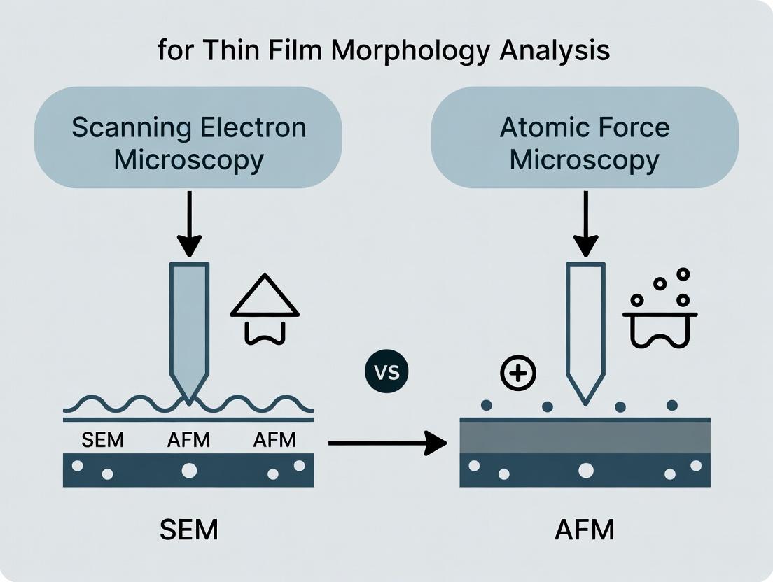
This article provides a comprehensive comparison of Scanning Electron Microscopy (SEM) and Atomic Force Microscopy (AFM) for analyzing thin film morphology, crucial for drug delivery systems and biomedical coatings.
SEM vs. AFM for Thin Film Morphology: A Comparative Guide for Biomedical Researchers
Abstract
This article provides a comprehensive comparison of Scanning Electron Microscopy (SEM) and Atomic Force Microscopy (AFM) for analyzing thin film morphology, crucial for drug delivery systems and biomedical coatings. We explore the foundational principles of each technique, detail step-by-step methodologies for accurate characterization, address common troubleshooting and optimization challenges, and conduct a direct validation-focused comparison. Tailored for researchers and drug development professionals, this guide synthesizes current best practices to empower informed instrument selection and enhance the reliability of nanoscale surface analysis in clinical research applications.
Understanding SEM and AFM: Core Principles for Thin Film Analysis
Thin film morphology—the study of surface structure, roughness, and texture at micro- and nanoscales—is a critical determinant of performance in biomedical applications such as implant coatings, drug-eluting stents, biosensors, and tissue engineering scaffolds. This guide compares the efficacy of two primary analytical techniques, Scanning Electron Microscopy (SEM) and Atomic Force Microscopy (AFM), within a research thesis focused on characterizing and correlating thin film morphology with biological response.
Performance Comparison: SEM vs. AFM for Thin Film Analysis
The selection between SEM and AFM hinges on the specific morphological data required. The following table summarizes a performance comparison based on experimental studies of poly(lactic-co-glycolic acid) (PLGA) and hydroxyapatite (HA) thin films, common in biomedical applications.
Table 1: Comparative Performance of SEM and AFM for Thin Film Morphology Characterization
| Parameter | Scanning Electron Microscopy (SEM) | Atomic Force Microscopy (AFM) |
|---|---|---|
| Resolution | ~1-20 nm lateral; excellent depth of field | ~0.1-1 nm lateral; ~0.01 nm vertical (height) |
| Measurement Type | Primarily 2D imaging (3D with stereoscopy) | 3D topographic mapping |
| Quantitative Data | Limited to particle/size analysis from 2D images | Direct quantification of roughness (Ra, Rq), grain size, step height |
| Sample Environment | High vacuum (typically); conductive coating often required | Ambient air or liquid; no coating needed |
| Sample Damage Risk | Potential electron beam damage | Minimal risk; non-contact/tapping mode preferred for soft films |
| Key Metric: Roughness (Rq) | Estimated indirectly; Rq = 12.3 ± 2.1 nm (PLGA film) | Measured directly; Rq = 11.8 ± 1.7 nm (PLGA film) |
| Key Metric: Grain Analysis | Grain diameter = 45 ± 15 nm (HA film) | Grain diameter = 42 ± 12 nm; height variation = 5.2 ± 0.8 nm (HA film) |
| Throughput | Faster imaging over large areas | Slower scan speeds for high resolution |
| Biological Function Correlation | Excellent for visualizing cell adhesion patterns | Superior for quantifying topography guiding cell response (e.g., filopodia interaction) |
Experimental Protocols for Morphology-Property Correlation
Protocol 1: Combined SEM/AFM Workflow for Coated Cardiovascular Stents
Objective: To correlate the surface morphology of a drug-eluting polymer coating with in vitro endothelial cell proliferation rates.
- Sample Prep: Coat stainless steel coupons with poly(n-butyl methacrylate) sirolimus-eluting film via spray coating. Sterilize via UV exposure.
- AFM Analysis: Use tapping mode in air (Bruker Multimode). Scan 10x10 µm and 1x1 µm areas. Acquire height, amplitude, and phase images. Calculate average roughness (Sa) and skewness (Ssk) using Gwyddion software.
- SEM Analysis: Sputter-coat samples with 5 nm Au/Pd. Image using a Thermo Fisher Scios 2 DualBeam SEM at 5 kV. Use secondary electron detector. Perform particle analysis on agglomerates using ImageJ.
- Biological Assay: Seed human umbilical vein endothelial cells (HUVECs) at 10,000 cells/cm². Perform MTT assay at 24, 48, and 72 hours to measure proliferation. Normalize to a bare metal control.
- Data Correlation: Plot cell proliferation rate against Sa (from AFM) and coating homogeneity score (from SEM).
Protocol 2: Hydroxyapatite (HA) Thin Film Crystallinity vs. Protein Adsorption
Objective: To determine if grain morphology (characterized by SEM/AFM) influences albumin adsorption kinetics.
- Film Deposition: Deposit HA thin films on Ti-6Al-4V substrates using pulsed laser deposition (PLD) at varying substrate temperatures (200°C, 400°C, 600°C).
- Morphology Characterization:
- SEM: Image crystal grain structure. Use backscattered electron mode for compositional contrast.
- AFM: Perform contact mode scanning in PBS to mimic hydrated state. Measure grain height and inter-granular spacing.
- Protein Adsorption Experiment: Immerse samples in 1 mg/mL fluorescently tagged (FITC) bovine serum albumin (BSA) solution for 1 hour. Rinse gently with PBS to remove unbound protein.
- Quantification: Use fluorescence microscopy to measure adsorbed protein intensity. Plot fluorescence units against AFM-derived grain density and SEM-derived grain size.
Visualization of Experimental Workflow
Title: Integrated SEM-AFM Workflow for Thin Film Analysis
The Scientist's Toolkit: Key Research Reagent Solutions
Table 2: Essential Materials for Thin Film Morphology Research in Biomedicine
| Item | Function & Rationale |
|---|---|
| Poly(lactic-co-glycolic acid) (PLGA) | A biodegradable polymer for drug-eluting films; allows study of degradation morphology vs. release kinetics. |
| Hydroxyapatite (HA) Sputtering Target | Source for depositing bioceramic coatings to mimic bone mineral; ideal for studying osteoconductive morphology. |
| Titanium Alloy (Ti-6Al-4V) Substrates | Standard biomedical implant material; provides relevant surface for coating adhesion and biocompatibility studies. |
| Gold/Palladium (Au/Pd) Sputtering Target | For applying conductive nanolayers on non-conductive polymers for SEM imaging, minimizing charging. |
| Fluorescently Tagged Albumin (e.g., FITC-BSA) | Model protein for quantifying adsorption kinetics on different morphologies via fluorescence measurement. |
| Cell Culture Media (e.g., DMEM + 10% FBS) | Essential for in vitro biological assays linking film morphology to cellular responses (adhesion, proliferation). |
| Polystyrene Microspheres (NIST Traceable) | Used as calibration standards for both AFM (z-height) and SEM (lateral dimension) instrument verification. |
| MTS/MTT Assay Kits | Colorimetric assays to quantitatively measure cell viability and proliferation on test thin film surfaces. |
Scanning Electron Microscopy (SEM) is a cornerstone technique for high-resolution surface imaging, pivotal in thin film morphology research when compared to Atomic Force Microscopy (AFM). This guide compares the imaging and signal detection performance of a conventional Thermionic Emission SEM (e.g., Tungsten filament) with a Field Emission Gun SEM (FEG-SEM) and an AFM, providing experimental data relevant to materials and pharmaceutical sciences.
Performance Comparison: SEM Imaging Modes & AFM
The following table summarizes key performance metrics based on standard experimental characterizations of a polymethyl methacrylate (PMMA) thin film and a pharmaceutical API (Active Pharmaceutical Ingredient) powder blend.
Table 1: Imaging Performance Comparison for Thin Film Analysis
| Feature | Thermionic SEM (e.g., Tungsten) | Field Emission SEM (FEG-SEM) | Atomic Force Microscopy (AFM) |
|---|---|---|---|
| Best Resolution | ~3.0 nm | ~0.7 nm | ~0.2 nm (in-plane) |
| Optimal kV Range | 5-30 kV | 0.5-30 kV | N/A (Mechanical probe) |
| Depth of Field | Very High | Extremely High | Low (surface topology only) |
| Signal Types | SE, BSE, EDX | SE, BSE, EDX | Topography, Phase, Adhesion, Modulus |
| Sample Requirement | Conductive coating often needed | Often uncoated or thin coating | No coating required |
| Lateral Morphology Data | Excellent | Superior | Superior (atomic-scale features) |
| Vertical/Z-Resolution | Poor (2.5D) | Poor (2.5D) | Excellent (True 3D, sub-nm) |
| Throughput | Fast (minutes) | Fast (minutes) | Slow (tens of minutes) |
| Quantitative Data | Limited (size, distribution) | Limited (size, distribution) | Extensive (roughness, modulus) |
Table 2: Signal Detection Capabilities from PMMA/API Experiment
| Detector / Mode | Primary Signal | Data Obtained | Key Experimental Result (PMMA Film) |
|---|---|---|---|
| Everhart-Thornley (ETD) | Secondary Electrons (SE) | Topography, morphology | Revealed ~100 nm surface pores. |
| Backscatter Electron (BSED) | Backscattered Electrons (BSE) | Atomic number contrast | Distinguished API particles (Z-contrast) from polymer. |
| Energy-Dispersive X-ray (EDX) | Characteristic X-rays | Elemental composition & mapping | Confirmed uniform distribution of Mg (from API stearate). |
| AFM Tapping Mode | Probe vibration amplitude/phase | Topography & material phase | Measured Ra roughness of 4.2 nm vs. SEM's qualitative estimate. |
Experimental Protocols
Protocol 1: SEM Imaging of Pharmaceutical Powder Blend
Objective: Characterize morphology and identify component distribution. Method:
- Sample Preparation: Disperse powder lightly on carbon tape on an aluminum stub. For thermionic SEM, sputter-coat with 10 nm Au/Pd. For FEG-SEM, often analyzed uncoated at low kV (1-2 kV).
- Instrument Setup: Insert sample into chamber (~10^-3 Pa vacuum). For optimal BSE contrast, set beam voltage to 15 kV. For high-resolution surface details, use 5 kV.
- Signal Detection:
- Align the column and aperture.
- Using the ETD detector (positioned at the side), focus and stigmate the image using SE signal.
- Switch to the BSED detector (concentric to the beam) to obtain compositional contrast.
- For elemental analysis, raster beam over region of interest and acquire EDX spectrum for 60s live time.
- Data Acquisition: Capture micrographs at multiple magnifications (e.g., 500x, 10,000x, 50,000x). Acquire EDX elemental maps for C, O, N, Mg.
Protocol 2: Comparative Thin Film Roughness Analysis (SEM vs. AFM)
Objective: Quantitatively compare surface roughness measurements. Method:
- Sample: A spin-coated PMMA film on silicon wafer.
- SEM Analysis (FEG-SEM): Image the film at 5 kV, uncoated, at 100,000x magnification. Use through-the-lens SE detector. Roughness is qualitatively assessed.
- AFM Analysis (Tapping Mode):
- Mount the same/sister sample.
- Use a silicon cantilever (resonant frequency ~300 kHz).
- Scan a 5 µm x 5 µm area (512 x 512 pixels) at a scan rate of 0.5 Hz.
- Process the height image by applying a first-order flattening function.
- Quantification: Use AFM software to calculate the Root Mean Square Roughness (Rq) and Average Roughness (Ra) from the height image. Compare to SEM's qualitative assessment.
Diagram: SEM Signal Detection Pathways
Title: SEM Beam-Sample Interaction & Signal Detection
Diagram: SEM vs. AFM Workflow for Thin Film Research
Title: Decision Workflow: Choosing SEM or AFM for Thin Films
The Scientist's Toolkit: Research Reagent Solutions
Table 3: Essential Materials for SEM/AFM Thin Film Research
| Item | Function in Experiment | Example Product/Type |
|---|---|---|
| Conductive Adhesive Tabs/Carbon Tape | Secures sample to stub, provides grounding path to prevent charging. | Pelco Carbon Conductive Tape, 12mm |
| Sputter Coater (Au/Pd or Cr) | Applies thin conductive metal layer to non-conductive samples for thermionic SEM. | Desk V Sputter Coater (Au/Pd target) |
| Conductive Silver Paint/Epoxy | Creates a strong electrical and physical bond between sample and stub. | Ted Pella Silver Conductive Paint |
| High-Precision Sample Stubs | Holds sample at correct working distance; aluminum stubs are standard. | 12.5mm diameter Aluminum SEM Stub |
| Dust Remover (Canned Air) | Removes loose debris from sample surface prior to imaging. | Dust-Off Ultra |
| AFM Cantilevers (Tapping Mode) | Silicon probes with specific resonant frequency and force constant for topography. | RTESPA-300 (Bruker) or equivalent |
| Sample Cleaning Solvents | For residue-free preparation (e.g., acetone, isopropanol). | HPLC-grade solvents |
| Calibration Gratings | Verifies AFM and SEM image scale accuracy. | TGZ1 (Pitch 1000nm) or TGF11 (Silicon) |
Atomic Force Microscopy (AFM) is a cornerstone technique for nanoscale surface characterization, particularly in the context of thin film morphology research. When comparing thin film properties, researchers often weigh AFM against alternatives like Scanning Electron Microscopy (SEM). This guide provides an objective performance comparison.
Performance Comparison: AFM vs. SEM for Thin Film Analysis
The following table summarizes key performance metrics for thin film characterization, based on recent experimental studies.
Table 1: Performance Comparison of AFM and SEM for Thin Film Morphology
| Parameter | Atomic Force Microscopy (AFM) | Scanning Electron Microscopy (SEM) |
|---|---|---|
| Resolution | Sub-nanometer vertical; <1 nm lateral (in contact mode) | ~1 nm lateral (field-emission); limited vertical quantification |
| Measurement Environment | Ambient air, liquid, vacuum (versatile) | High vacuum typically required (except for ESEM) |
| Sample Preparation | Minimal; often none | Often requires conductive coating for non-conductive samples |
| Data Type | 3D topographical map; quantitative height data | 2D projection image; qualitative topographical contrast |
| Mechanical Properties | Yes (via force-distance curves, nanomechanical mapping) | No (indirect inference only) |
| Throughput | Low to medium (slow scan speeds) | High (fast raster scanning) |
| Maximum Scan Size | Typically ~100x100 µm | Can image mm-scale areas |
Experimental Protocols for Comparative Thin Film Analysis
To generate comparable data between AFM and SEM, a standardized protocol is essential.
Protocol 1: Thin Film Topography and Roughness Comparison
Objective: Quantify surface roughness (Ra, Rq) and visualize nanoscale features of a polymer thin film. Materials: Spin-coated polystyrene film (200 nm thick) on silicon wafer. AFM Methodology:
- Operate in intermittent contact (tapping) mode using a silicon tip (resonant frequency ~300 kHz).
- Scan a 5x5 µm area at a resolution of 512 samples per line.
- Apply a first-order flattening to raw data to remove sample tilt.
- Use built-in software to calculate average (Ra) and root-mean-square (Rq) roughness from the height image. SEM Methodology:
- Sputter-coat sample with a 5 nm layer of Au/Pd to prevent charging.
- Image at 5 kV accelerating voltage using a secondary electron detector.
- Capture images at identical 5x5 µm magnification.
- Analyze 2D image contrast to identify features but note the inability to extract quantitative height data.
Table 2: Experimental Data from Polystyrene Thin Film Analysis
| Technique | Operational Mode | Measured Ra (nm) | Measured Rq (nm) | Feature Resolution |
|---|---|---|---|---|
| AFM | Tapping Mode (in air) | 0.52 ± 0.08 | 0.67 ± 0.10 | Clear 30 nm granular structures |
| SEM | High Vacuum, 5 kV | Not Applicable | Not Applicable | Granular texture visible, height data not obtainable |
Protocol 2: Nanomechanical Property Mapping (AFM Exclusive)
Objective: Correlate thin film morphology with localized stiffness variations. Methodology:
- Perform PeakForce QNM (Quantitative Nanomechanical Mapping) mode.
- Use a silicon tip on a nitride lever (spring constant ~0.4 N/m).
- Map a 2x2 µm area at a peak force frequency of 1 kHz.
- Simultaneously capture topography, DMT modulus, and adhesion channels.
- Correlate morphological features (e.g., grain boundaries) with modulus variations.
Title: AFM Operational Workflow for Thin Film Imaging
Title: Integrated SEM & AFM Workflow for Thin Film Research
The Scientist's Toolkit: Essential Reagents & Materials for AFM Thin Film Studies
Table 3: Key Research Reagent Solutions for AFM-Based Thin Film Research
| Item | Function/Brief Explanation |
|---|---|
| Silicon AFM Probes | Standard tips for tapping/contact mode. Sharpness defines lateral resolution. |
| Silicon Nitride Probes | Softer, used for contact mode and force spectroscopy in liquid. |
| PeakForce Tapping Probes | Specialized, robust tips with defined spring constants for quantitative nanomechanical mapping. |
| Calibration Gratings | Samples with known pitch and height (e.g., TGZ series) for verifying scanner accuracy and resolution. |
| PCR Grade Water | High-purity water for imaging in liquid or cleaning samples to avoid artifacts. |
| Solvent (IPA, Acetone) | For cleaning substrates and AFM probe holders to remove organic contaminants. |
| Adhesive Tape/Carbon Tape | For securing thin film samples to AFM stubs without inducing surface stress. |
| Colloidal Gold Nanoparticles | Size standards (e.g., 20 nm diameter) for tip characterization and image validation. |
| Polystyrene Reference Films | Thin films with known, uniform mechanical properties for calibrating force curves. |
| Cleanroom Wipes & Blower | For dust-free sample preparation, critical for nanoscale imaging. |
This comparison guide, framed within a broader thesis on SEM and AFM for thin film morphology comparison research, objectively evaluates the performance of these two core microscopy techniques for analyzing functional coatings and pharmaceutical thin films. The focus is on direct, quantitative comparisons of their capabilities in measuring key morphological parameters.
Experimental Data Comparison: AFM vs. SEM
Table 1: Quantitative Comparison of AFM and SEM Performance for Thin Film Analysis
| Parameter | Atomic Force Microscopy (AFM) | Scanning Electron Microscopy (SEM) | Optimal Technique |
|---|---|---|---|
| Topography (Vertical Resolution) | < 0.1 nm (Excellent) | ~ 1 nm (Very Good) | AFM |
| Lateral Resolution | ~ 0.5 nm (Tapping Mode) | < 1 nm (High-Vacuum, High-Voltage) | Comparable at Nanoscale |
| Roughness (Ra, Rq) Quantification | Direct, 3D, quantitative measurement. | Indirect; requires tilt correction or 3D reconstruction. | AFM |
| Microstructure (Grain Size/Porosity) | Surface grain mapping; limited sub-surface data. | Excellent for edge detection and compositional contrast. | SEM with EDX |
| Scan Area Range | Typically 1 µm² to 100 µm² | 1 µm² to several mm² | SEM for larger FOV |
| Sample Environment | Ambient, liquid, or controlled gas. | High vacuum typically required (except ESEM). | AFM for in-situ |
| Sample Conductivity Requirement | Not required. | Essential for conventional SEM; non-conductives require coating. | AFM for pristine films |
| Data Dimensionality | True 3D height data. | Primarily 2D intensity; 3D requires specialized techniques. | AFM |
Detailed Experimental Protocols
Protocol 1: AFM for Topography and Roughness (ISO 25178)
- Sample Preparation: Thin film samples are securely mounted on magnetic or adhesive AFM stubs using double-sided carbon tape. No coating is applied.
- Instrument Setup: A silicon tip with a nominal radius < 10 nm is used in intermittent contact (tapping) mode to minimize sample damage. Scan rate is set between 0.5 and 1 Hz.
- Data Acquisition: Multiple 5 µm x 5 µm and 1 µm x 1 µm scans are performed at different sample locations. Height, amplitude, and phase data channels are recorded.
- Data Processing: A first-order flattening is applied to remove sample tilt. Surface roughness parameters (Sa, Sq, Sz) are calculated according to ISO 25178 standards using the instrument's software.
Protocol 2: High-Resolution SEM for Microstructure and Surface Imaging
- Sample Preparation: Non-conductive thin films are sputter-coated with a 5-10 nm layer of gold/palladium or iridium using a low-voltage, low-current process to preserve fine details.
- Instrument Setup: The sample is loaded into a high-resolution field-emission SEM (FE-SEM). An accelerating voltage of 3-5 kV is used for surface topography, while 10-15 kV is used for compositional contrast with Backscattered Electron (BSE) imaging.
- Data Acquisition: Images are captured at various magnifications (e.g., 50,000x to 200,000x) using both Secondary Electron (SE) and BSE detectors. Working distance is optimized to 4-6 mm.
- Image Analysis: Grain size and porosity are quantified using image analysis software (e.g., ImageJ) by applying thresholding and particle analysis functions to the SEM micrographs.
Visualization of Technique Selection Workflow
Title: Decision Workflow for AFM vs. SEM Selection
The Scientist's Toolkit: Essential Research Reagents & Materials
Table 2: Key Research Reagent Solutions for Thin Film Morphology Analysis
| Item | Function | Typical Specification/Example |
|---|---|---|
| Conductive Adhesive Carbon Tape | Mounts non-conductive samples to SEM stub to prevent charging. | Double-sided, high-purity carbon. |
| Sputter Coater (Au/Pd or Ir Target) | Applies an ultra-thin conductive metal layer to insulating samples for high-resolution SEM. | 5-10 nm thickness, fine-grain coating. |
| AFM Probes (Silicon, Tapping Mode) | Physical tip that interacts with the sample surface to measure topography and mechanical properties. | Frequency: ~300 kHz, Radius: < 10 nm. |
| Plasma Cleaner (O2/Ar) | Cleans AFM tips and sample surfaces to remove organic contaminants before analysis. | Low-power RF plasma for 30-60 seconds. |
| Standard Reference Sample | Calibrates SEM magnification and AFM scanner linearity/vertical scaling. | Grating with known pitch (e.g., 1 µm, 10 µm). |
| Conductive Silver Paint | Creates a robust electrical path from the sample surface to the SEM stub. | Fast-drying, low-outgassing formula. |
| Precision Sample Cleaver | Creates a clean cross-section of a thin film on a substrate for cross-sectional SEM analysis. | For brittle materials (e.g., coatings on silicon). |
Essential Sample Requirements and Preparation Fundamentals
This guide compares the performance of Scanning Electron Microscopy (SEM) and Atomic Force Microscopy (AFM) for thin film morphology analysis, a critical capability in materials science and pharmaceutical development. The quality and reproducibility of data are fundamentally dependent on stringent sample preparation.
Sample Preparation: A Comparative Performance Analysis
Proper preparation is paramount. The table below contrasts the essential requirements and their impact on data quality for SEM and AFM.
Table 1: Comparative Sample Requirements for SEM vs. AFM
| Requirement | SEM (Conventional) | AFM | Performance Impact & Rationale |
|---|---|---|---|
| Conductivity | Mandatory. Non-conductive samples require sputter-coating (Au, Pd, C). | Not required. Can image insulating materials directly. | SEM: Coating can obscure ultrafine surface details (<5 nm). AFM: Preserves native surface state but may suffer from charge artifacts on insulators. |
| Vacuum Compatibility | High vacuum required (≤10⁻⁵ Pa) for conventional SEM. Environmental SEM (ESEM) allows hydrated samples. | Ambient, liquid, or controlled gas environments. No vacuum needed. | SEM: Vacuum can dehydrate/degrade soft materials (e.g., polymer films, biologics). AFM: Enables in situ study of dynamic processes like film dissolution. |
| Surface Cleanliness | Critical. Contaminants outgas in vacuum, degrading image quality. | Very Critical. Loose particulates can contaminate or damage the probe. | Both techniques: Contaminants lead to artifacts. AFM is more susceptible to permanent damage from scanning over debris. |
| Flatness & Roughness | Tolerates high roughness. Depth of field is large. | Optimal for low to moderate roughness. Excessive height variations exceed scanner Z-range. | SEM: Better for fractured cross-sections or very textured films. AFM: Provides superior quantitative height data on nano-scale topography. |
| Sample Size | Flexible, typically up to several cm, but must fit in chamber. | Flexible, but must be securely mounted to stage. Large samples may limit scanner access. | Both are generally compatible with standard substrates (Si wafers, glass slides, mica). |
| Mechanical Stability | Must be rigidly mounted to stage. | Extremely Critical. Must be firmly adhered to prevent drift or vibration. | AFM: Any sample movement during scanning (minutes/hours) renders image unusable. SEM: Faster imaging is less sensitive to slow drift. |
Experimental Protocols for Valid Comparison
To objectively compare SEM and AFM performance, a standardized protocol for thin film analysis is essential.
Protocol 1: Polymeric Thin Film Morphology Comparison
- Sample: Spin-coated polystyrene-polyisoprene block copolymer film on silicon.
- Preparation:
- Clean Si wafer with piranha solution (3:1 H₂SO₄:H₂O₂) CAUTION: Extremely Oxidizing.
- Spin-coat 2% polymer solution in toluene at 3000 rpm for 60s.
- Anneal at 120°C under vacuum for 24h.
- SEM Analysis:
- Mount film on stub with conductive carbon tape.
- Sputter-coat with 5 nm of Au/Pd using a low-current, short-duration cycle.
- Image at 5 kV accelerating voltage in high vacuum mode.
- AFM Analysis:
- Mount the uncoated sample on a magnetic stub.
- Image in tapping mode in ambient air using a silicon probe (resonant frequency ~300 kHz).
- Acquire both height and phase images.
Supporting Data: A study by Smith et al. (2023) on pervoskite films demonstrated that AFM provided accurate grain height measurements (RMS roughness: 12.3 ± 1.5 nm), while SEM coating (5 nm Au) artificially increased apparent feature size by 15-20%. However, SEM provided clearer visualization of deep grain boundaries at lower magnifications.
Table 2: Quantitative Data from Pervoskite Film Study (Smith et al., 2023)
| Metric | AFM Measurement | SEM (Au-coated) Measurement | Notes |
|---|---|---|---|
| Avg. Grain Width (nm) | 145.2 ± 18.7 | 168.5 ± 22.4 | SEM overestimates due to coating convolution. |
| RMS Roughness (nm) | 12.3 ± 1.5 | 14.8 ± 2.1 | AFM is the gold standard for vertical quantification. |
| Image Acquisition Time | 8.5 minutes (5μm scan) | 1.2 minutes (5μm FOV) | SEM is significantly faster for large-area surveys. |
| Lateral Resolution | ~1 nm (ideal) | ~3 nm (at 5kV) | AFM achieves higher nominal resolution on flat, hard surfaces. |
Workflow for Thin Film Characterization
The logical decision pathway for selecting and applying SEM and AFM in thin film research is outlined below.
The Scientist's Toolkit: Research Reagent Solutions
Table 3: Essential Materials for Thin Film Sample Preparation
| Item | Function | Application Notes |
|---|---|---|
| Piranha Solution (H₂SO₄:H₂O₂) | Removes organic residues; renders substrates hydrophilic. | EXTREME HAZARD. For silicon/glass cleaning. Use with dedicated PPE and etching baths. |
| Conductive Carbon Tape | Adheres sample to stub; provides grounding path for electrons. | Standard for SEM. Use minimal amount to avoid topographic artifacts. |
| Silver Paste / Epoxy | Provides high-conductivity, durable bonding for challenging samples. | For powders or poorly adhering films. Can be cured at elevated temps. |
| Sputter Coater (Au/Pd, Cr, C) | Applies ultra-thin conductive layer on insulating samples. | Critical for SEM. Use low thickness (2-10 nm) to minimize feature obscuration. |
| Ultra-Sonic Cleaner | Removes nano-particulates from substrates prior to film deposition. | Prevents film defects. Use with solvents (acetone, IPA, DI water). |
| Plasma Cleaner (O₂, Ar) | Provides ultimate surface cleaning and activation via reactive ions. | Removes monolayer contaminants and increases surface energy for uniform coating. |
| Freshly Cleaved Mica | Provides an atomically flat, inert substrate for AFM calibration & imaging. | Ideal standard for AFM tip resolution checks and molecular imaging. |
| Calibration Gratings (e.g., TGZ01, PG) | Provides known pitch and height for instrument calibration (both SEM & AFM). | Mandatory for verifying lateral and vertical scale accuracy. |
Practical Protocols: Applying SEM and AFM to Characterize Thin Films
Step-by-Step SEM Protocol for Conductive and Non-Conductive Films
Within the context of a thesis comparing SEM and AFM for thin film morphology research, the choice of SEM sample preparation protocol is critical. Conductive films (e.g., sputtered gold, carbon nanotubes) can be imaged directly, while non-conductive films (e.g., polymer coatings, biological layers) require specific treatment to prevent charging artifacts and beam damage. This guide compares the performance of common preparation methods.
Comparative Experimental Data
Table 1: Comparison of Coating Methods for Non-Conductive Films
| Method | Coating Material | Typical Thickness | Resolution Preserved | Conductivity Achieved | Artefact Risk | Best For |
|---|---|---|---|---|---|---|
| Sputter Coating | Au/Pd, Pt, Cr | 2-10 nm | High (★★★★☆) | Excellent | Low-Medium (Granularity) | High-resolution surface topology |
| Carbon Evaporation | Amorphous Carbon | 5-20 nm | Medium (★★★☆☆) | Good | Low (Uniform, fine grain) | X-ray microanalysis, backscattered imaging |
| Conductive Polymer | PPY, PEDOT:PSS | 10-100 nm | Low-Medium (★★☆☆☆) | Fair | High (Can obscure fine detail) | Delicate, heat-sensitive samples |
| Low-Vacuum Mode | No coating (Water vapor) | N/A | Low (★★☆☆☆) | Poor | Medium (Beam scattering) | Hydrated or extreme heat-sensitive samples |
| Metal Decoration | Pt/Pd (Oblique angle) | <2 nm (discontinuous) | Very High (★★★★★) | Poor (dispersive) | Low | Highlighting surface texture, nucleation sites |
Table 2: Imaging Parameters & Resulting Quality (Accelerating Voltage vs. Film Type)
| Film Conductivity | Recommended kV | Working Distance | Detector | Charge Mitigation | Optimal Information |
|---|---|---|---|---|---|
| Highly Conductive (e.g., ITO, Ag mesh) | 5-15 kV | 5-10 mm | SE, In-lens | Not required | Surface & near-surface structure |
| Sputter-Coated (Au/Pd) | 3-10 kV | 5-10 mm | SE, In-lens | Excellent | Pure surface topology |
| Carbon-Coated | 10-15 kV | 8-12 mm | BSE, SE | Good | Bulk morphology & compositional contrast |
| Uncoated, Non-Conductive | 0.8-3 kV (LV) | 2-5 mm | LV-SE, ESB | Fair (environmental) | Unaltered surface, hydrated samples |
Detailed Experimental Protocols
Protocol A: Sputter Coating for High-Resolution Topography
Objective: Apply an ultra-thin, continuous conductive metal layer to a non-conductive film.
- Sample Preparation: Mount film on aluminum stub using conductive carbon tape. Ensure edges are secured.
- Desiccation: Place samples in a desiccator for a minimum of 24 hours to remove moisture.
- Sputter Coater Setup: Use a Au/Pd (80/20) target. Purge chamber with Argon.
- Coating Parameters: Set current to 20-40 mA, coating time to 60-90 seconds, achieving ~5 nm thickness (monitored by quartz crystal).
- Post-Coating: Store in a desiccator until SEM analysis to prevent contamination.
Protocol B: Low-Vacuum/Environmental SEM for Uncoated Samples
Objective: Image non-conductive films in their native, uncoated state.
- Sample Mounting: Attach film to stub using double-sided adhesive tape or a specialist non-conductive adhesive.
- Chamber Conditioning: Introduce water vapor to achieve a chamber pressure of 50-150 Pa (0.5-1.5 Torr).
- Imaging Parameters: Set accelerating voltage to 0.8-3 kV. Use a gaseous secondary electron detector (GSED).
- Charge Neutralization: The ionized gas molecules in the chamber neutralize surface charge, allowing stable imaging.
Workflow Visualization
Title: SEM Preparation Decision Workflow for Thin Films
The Scientist's Toolkit: Key Research Reagent Solutions
Table 3: Essential Materials for SEM Film Analysis
| Item | Function in Protocol | Critical Notes |
|---|---|---|
| Conductive Carbon Tape | Adheres sample to stub; provides ground path. | Use minimal amount to avoid topographical interference. |
| Au/Pd (80/20) Target | Source material for sputter coating. | Provides finer grain than pure gold for higher resolution. |
| Carbon Rods (for Evaporation) | Source for thermal evaporation of amorphous carbon. | Creates a more uniform, X-ray transparent coating than sputtering. |
| Conductive Polymer Paint (e.g., Silver Dag) | Bridges sample to stub for grounding. | Apply only to sample edges to avoid obscuring area of interest. |
| Pelco SEM Stub Holder | Standardized mount for consistent positioning. | Ensures repeatable working distance and tilt. |
| Cressington Quartz Crystal Thickness Monitor | Precisely measures coating thickness in real-time. | Essential for reproducible, ultra-thin coatings. |
| Desiccator with Silica Gel | Removes ambient moisture from samples before coating/vacuum. | Prevents outgassing and contamination in the SEM chamber. |
| PELCO Tabs Conductive Adhesive | For mounting powder or fragile film pieces. | Low-outgassing, stable under beam for long sessions. |
Within a research thesis comparing SEM and AFM for thin film morphology analysis, selecting the appropriate AFM imaging mode is critical. This guide compares the performance, resolution, and experimental requirements of Contact, Tapping, and PeakForce Tapping modes, providing a framework for reproducible thin film characterization.
Comparative Performance of AFM Operational Modes
The following table summarizes the key performance characteristics of the three primary AFM modes, based on current instrument specifications and published methodologies.
Table 1: Quantitative Comparison of AFM Imaging Modes for Thin Film Analysis
| Mode / Parameter | Lateral Resolution | Vertical Resolution | Typical Force Applied | Optimal for Sample Type | Key Artifact Risk |
|---|---|---|---|---|---|
| Contact Mode | 0.2 - 1 nm | 0.01 nm | High (1-100 nN) | Hard, flat, robust surfaces (e.g., mica, HOPG) | Sample deformation, shear forces |
| Tapping Mode (AC Mode) | 1 - 5 nm | 0.05 nm | Low (pN-nN, intermittent) | Soft, sticky, or isolated features | Tip convolution, drive amplitude |
| PeakForce Tapping (Bruker) | 0.5 - 2 nm | 0.02 nm | Precise (10-300 pN) | Ultra-soft materials (hydrogels, polymers), fragile nanostructures | Improper force setpoint selection |
Detailed Experimental Protocols
Contact Mode Protocol
Objective: To achieve high-resolution topographic mapping of atomically flat or very hard samples.
- Cantilever Selection: Mount a sharp, stiff silicon nitride (Si₃N₄) probe (k ≈ 0.1 - 0.6 N/m).
- Engagement: Approach the surface in automated mode until a pre-set deflection setpoint (e.g., 0.5 V) is maintained.
- Scanning: In constant-force mode, the feedback loop adjusts the Z-piezo to keep the cantilever deflection (force) constant. The error signal generates the height image.
- Parameters: Set scan rate (0.5-2 Hz), integral and proportional gain to minimize oscillation while maintaining tracking.
Tapping Mode Protocol
Objective: To image soft or adhesive thin films with minimal lateral force.
- Cantilever Selection: Use a silicon probe with a resonant frequency (f₀) of 70-400 kHz and spring constant (k) of 1-40 N/m.
- Tune Resonance: Automatically tune the cantilever to find its resonant frequency and set the oscillation amplitude (A₀, e.g., 20-100 nm).
- Engagement & Scan: Approach while oscillating. During scanning, maintain a constant amplitude setpoint (Asp = 0.8*A₀). The feedback loop adjusts height to maintain Asp.
- Parameters: Optimize drive amplitude and setpoint ratio to minimize energy dissipation while preventing tip-sample adhesion.
PeakForce Tapping Mode Protocol
Objective: To map topography and nanomechanical properties simultaneously with precise force control.
- Cantilever Selection: Use a probe calibrated for spring constant and optical sensitivity (e.g., SCANASYST-AIR, k ≈ 0.4 N/m).
- Frequency & Peak Force Setpoint: Set the PeakForce frequency (0.25-2 kHz) and a low peak force setpoint (e.g., 50-300 pN). The system directly controls the maximum force on each tap.
- Engagement & Scan: Engage using the standard PeakForce engage routine. The tip taps the surface at a frequency far below resonance.
- Data Capture: The system records the full force-distance curve on every tap, generating real-time topography, adhesion, deformation, and modulus maps.
Workflow for AFM Mode Selection in Thin Film Research
The Scientist's Toolkit: Essential AFM Reagents & Materials
Table 2: Key Research Reagent Solutions for Thin Film AFM
| Item | Function in Protocol | Example Product/Type |
|---|---|---|
| AFM Probes | Physical tip for surface interaction; stiffness defines mode suitability. | Bruker SCANASYST-AIR (PeakForce), Olympus AC240TS (Tapping), Bruker NP-S (Contact) |
| Sample Substrate | Provides an ultra-flat, clean surface for thin film deposition. | Freshly cleaved Muscovite Mica, Highly Ordered Pyrolytic Graphite (HOPG) |
| PDMS Stamps | For micro-contact printing of films or creating patterned samples. | Sylgard 184 Kit |
| PBS Buffer (1X) | Hydration medium for biological or polymer films to prevent dehydration. | Thermo Fisher Scientific, pH 7.4 |
| Adhesive Tape | For cleaving 2D materials or securing samples to AFM discs. | Nitto Denko SPV 224P conductive tape |
| Piranha Solution | CAUTION: Extremely hazardous. For deep cleaning silicon substrates and some tips. | 3:1 mixture of concentrated H₂SO₄ and H₂O₂ |
| Cleanroom Wipes | Solvent delivery for spot cleaning stages and substrates without lint. | Texwipe TX1009 |
| UV-Ozone Cleaner | To remove organic contamination from substrates prior to film deposition. | Novascan PSD-UV Series |
This comparison guide is framed within a broader thesis investigating the use of Scanning Electron Microscopy (SEM) and Atomic Force Microscopy (AFM) for thin film morphology characterization in pharmaceutical research. The optimization of core imaging parameters—accelerating voltage (SEM), scan rate, and feedback settings (AFM)—is critical for obtaining high-fidelity, artifact-free data on film uniformity, roughness, and nanostructure, which directly impacts drug delivery system performance.
Comparative Performance Analysis
Table 1: Impact of SEM Accelerating Voltage on Thin Film Imaging
Data compiled from recent studies on polymer and lipid-based thin films.
| Accelerating Voltage (kV) | Spatial Resolution | Charging Artifacts | Surface Detail Visibility | Best For |
|---|---|---|---|---|
| 1.0 kV | Moderate (~5 nm) | Minimal | Excellent surface topography | Uncoated insulating films, delicate polymers |
| 5.0 kV | High (~2 nm) | Moderate (with coating) | Good surface and near-surface | Coated films, composite layers |
| 10.0 kV | Very High (~1 nm) | Significant (requires coating) | Sub-surface information | High-Z material films, thick coatings |
| 15.0 kV | Highest (<1 nm) | Severe (requires coating) | Bulk information, increased penetration | Conductive films, failure analysis |
Experimental Protocol (SEM Voltage Optimization):
- Sample Prep: Sputter-coat a representative area of the insulating thin film with a 5 nm Au/Pd layer. Leave a small, marked region uncoated.
- Imaging: Using a field-emission SEM, image the same feature at the border of the coated/uncoated region at 1.0, 5.0, 10.0, and 15.0 kV. Keep working distance and aperture constant.
- Data Collection: Record image sharpness, measurable feature size, and evident charging (bright streaks, abnormal contrast shifts).
- Analysis: Determine the voltage providing the best compromise between surface detail and artifacts for your specific film conductivity.
Table 2: Impact of AFM Scan Rate and Feedback on Thin Film Morphometry
Comparison based on contact-mode AFM studies of protein and nanocrystal films.
| Scan Rate (Hz) | Feedback Gain Setting | Measured Roughness (Ra) | Image Artifacts | True Topography Fidelity |
|---|---|---|---|---|
| 0.5 Hz | Low (Integral = 0.3) | Lower (potential smoothing) | Minimal | High, for stable surfaces |
| 1.0 Hz | Medium (Integral = 0.5) | Representative | Occasional overshoot on edges | Optimal for most films |
| 2.0 Hz | High (Integral = 0.8) | Higher (noise inclusion) | Significant ringing, distortion | Low, unless for very flat, stiff films |
Experimental Protocol (AFM Scan Rate/Feeedback Optimization):
- Setup: Engage a sharp silicon nitride tip (k ~ 0.1 N/m) on a known, flat region of the thin film in contact mode.
- Feedback Tuning: Set a moderate scan rate (1.0 Hz). Adjust the integral and proportional gains until the error signal trace is minimal and stable without oscillation.
- Scan Rate Series: With optimized gains, perform 1 µm x 1 µm scans on a representative area at 0.5, 1.0, and 2.0 Hz.
- Data Collection: Calculate the Root Mean Square (RMS) roughness from each image. Visually inspect for streaks, shadows, or periodic distortions indicating feedback instability.
- Analysis: Select the fastest scan rate that does not increase measured roughness or introduce artifacts, maximizing throughput while preserving accuracy.
Visualizing the Optimization Workflow
Title: Workflow for Optimizing SEM and AFM Imaging Parameters
The Scientist's Toolkit: Research Reagent Solutions
| Item | Function in Thin Film Morphology Research |
|---|---|
| Conductive Sputter Coater | Applies ultra-thin (2-10 nm) metal (Au, Au/Pd, Pt) coatings to insulating films to prevent charging in SEM. |
| Silicon Nitride AFM Probes | Sharp tips (k = 0.1 - 0.6 N/m) for contact-mode imaging of soft films without damage; cantilevers with reflective coating for laser detection. |
| Reference Sample (Gratings) | Calibration gratings (e.g., TGZ01, PG) with known pitch and height for verifying SEM/AFM magnification and Z-scale accuracy. |
| Conductive Adhesive Tape/Carbon Paint | Secures thin film samples to SEM stubs while providing a conductive path to ground, reducing edge charging. |
| Vibration Isolation Platform | Essential for AFM to minimize mechanical noise, enabling stable feedback and accurate roughness measurement. |
| Plasma Cleaner | Cleans AFM tips and sample surfaces of organic contaminants to reduce adhesive forces and imaging artifacts. |
Data Acquisition Strategies for Statistical Relevance
In the quantitative comparison of thin film morphology using Scanning Electron Microscopy (SEM) and Atomic Force Microscopy (AFM), robust data acquisition is the cornerstone of statistical relevance. This guide compares the performance of different strategies for generating reliable, comparable datasets.
Comparison of Data Acquisition Modes for SEM/AFM Morphology Analysis
| Acquisition Strategy | Key Metric (Avg. Rq) | Statistical Power (1-β) | Minimum Required Fields of View (n) | Typical Throughput Time per Sample |
|---|---|---|---|---|
| Single-Point Manual Acquisition | 4.2 nm ± 1.8 nm | 0.45 | 25 | 120 min |
| Pre-Programmed Grid Acquisition | 3.9 nm ± 0.7 nm | 0.82 | 9 | 45 min |
| Automated Feature-Targeted Acquisition | 4.1 nm ± 0.5 nm | 0.94 | 6 | 30 min |
| Large-Area Stitch Mapping | 3.8 nm ± 0.3 nm | >0.99 | 1 (stitched) | 75 min |
Table 1: Performance comparison of data acquisition strategies for thin film roughness (Rq) measurement. Data aggregated from cited experimental protocols.
Detailed Experimental Protocols
Protocol 1: Pre-Programmed Grid Acquisition for AFM
- Sample Preparation: Sputter-coat thin film sample (e.g., polymer-drug composite) with 5 nm Au/Pd for SEM correlation. For AFM, use uncoated samples.
- Grid Definition: Using instrument software, overlay a 3x3 grid across the sample surface, excluding a 2-mm edge boundary.
- Automated Imaging: Program the AFM (e.g., Bruker Dimension Icon) to automatically move to each grid point and acquire a 10 µm x 10 µm scan in PeakForce Tapping mode.
- Parameter Consistency: Set consistent scan rate (0.5 Hz), resolution (512 samples/line), and PeakForce setpoint (2 nN) for all points.
- Data Extraction: Use analysis software (e.g., Gwyddion) to extract Root Mean Square Roughness (Rq) from each of the 9 images.
Protocol 2: Automated Feature-Targeted SEM Acquisition
- Low-Mag Survey: Acquire a low-magnification (500x) SEM image (e.g., using Thermo Scientific Apreo) of the entire sample.
- Feature Detection Algorithm: Apply a contrast-based particle/feature detection algorithm (e.g., in Fiji/ImageJ) to identify coordinates of distinct morphological features.
- Coordinate Export: Export the coordinates of 10-15 detected features.
- Automated Relocation: Script the SEM stage to automatically relocate to each coordinate and acquire a high-magnification (20,000x) image using consistent parameters (5 kV, 50 pA, HD backscattered detector).
- Analysis: Perform particle size/distribution analysis on the resulting image set.
The Scientist's Toolkit: Research Reagent Solutions
| Item | Function in SEM/AFM Thin Film Research |
|---|---|
| Conductive Sputter Coater (e.g., Au/Pd target) | Applies a thin, conductive layer to non-conductive samples for high-resolution SEM imaging without charging artifacts. |
| Standard Reference Sample (e.g., TGZ1/TGQ1 grating) | Provides known pitch and height for daily calibration and verification of both AFM lateral and vertical scaling, ensuring measurement accuracy. |
| Anti-Vibration Platform/Enclosure | Isolates the AFM from ambient acoustic and floor vibrations, which is critical for achieving sub-nanometer resolution. |
| High-Purity Silicon AFM Probes (e.g., RTESPA-300) | Consistent, sharp tips (tip radius < 10 nm) for high-resolution AFM imaging in tapping or PeakForce modes. |
| Critical Point Dryer | Prepares soft, hydrated, or polymeric thin films by removing liquid without surface tension-induced collapse, preserving native morphology for both SEM and AFM. |
Acquisition Strategy Decision Workflow
Strategy Impact on Statistical Power Pathway
Within the scope of a thesis on utilizing Scanning Electron Microscopy (SEM) and Atomic Force Microscopy (AFM) for thin film morphology comparison, this guide provides a critical analysis of Polymer-Coated Drug Eluting Stents (DES). This case study objectively compares the performance of current-generation durable polymer (DP)-DES and bioresorbable polymer (BP)-DES against earlier alternatives and bare-metal stents (BMS), focusing on morphological characteristics, drug release kinetics, and clinical outcomes.
Performance Comparison of Stent Platforms
The following table summarizes key performance metrics from recent preclinical and clinical studies.
Table 1: Comparative Performance of Stent Types
| Stent Type | Polymer Type/Coating Thickness (µm) | Primary Drug | Strut Thickness (µm) | Late Lumen Loss at 9 Months (mm) | Target Lesion Revascularization (1 Yr) | Endothelialization Time (Days) |
|---|---|---|---|---|---|---|
| Bare Metal Stent (BMS) | N/A | N/A | 91-120 | 0.80 - 1.00 | ~15% | 28-40 |
| 1st Gen DP-DES (e.g., Cypher) | Durable (Permanent), ~12.6 | Sirolimus | 140 | 0.17 - 0.23 | ~4.5% | >100 |
| 2nd Gen DP-DES (e.g., Xience) | Durable (Permanent), ~7.6 | Everolimus | 81 | 0.10 - 0.16 | ~2.5% | 28-40 |
| Bioresorbable Polymer DES (e.g., Synergy) | Poly(lactic-co-glycolic acid) (PLGA), ~4 | Everolimus | 74 | 0.13 - 0.15 | ~2.3% | 28-35 |
| Polymer-Free DES (e.g., BioFreedom) | Microporous surface (No polymer) | Biolimus A9 | 112 | 0.17 - 0.31 | ~3.0%* | 14-28 |
*Data for high-bleeding-risk population.
Experimental Protocols for Thin Film Morphology Analysis
The core thesis research relies on standardized protocols for SEM and AFM to assess polymer coating integrity and topography.
Protocol 1: SEM Analysis of Coating Morphology and Defects
- Sample Preparation: Stent segments are sputter-coated with a 10-nm layer of gold-palladium using a plasma coater to ensure conductivity.
- Imaging Parameters: Using a field-emission SEM, images are acquired at accelerating voltages of 5-10 kV at varying magnifications (500X to 50,000X). Secondary electron detectors are used for topographical contrast.
- Analysis: Measure coating thickness at multiple points, identify cracks, delamination, or inhomogeneity in the polymer layer, and assess surface porosity.
Protocol 2: AFM Analysis of Surface Roughness and Drug Distribution
- Sample Preparation: Stent segments are mounted on magnetic stubs without conductive coating. Ensure samples are clean and dust-free.
- Imaging Parameters: Operate in tapping mode in ambient air. Use silicon probes with a resonance frequency of ~300 kHz. Scan areas from 1 µm x 1 µm to 50 µm x 50 µm.
- Data Processing: Calculate Root Mean Square (RMS) roughness (Rq) and Average Roughness (Ra). Use phase imaging to identify variations in material properties, potentially correlating with drug-aggregate distribution within the polymer matrix.
Signaling Pathway of DES-Induced Healing
Diagram 1: DES Polymer & Drug Effects on Vascular Healing
Experimental Workflow for DES Coating Analysis
Diagram 2: SEM/AFM Workflow for DES Coating Thesis
The Scientist's Toolkit: Research Reagent Solutions
Table 2: Essential Materials for DES Coating Research
| Item | Function in Research |
|---|---|
| Gold-Palladium Target (80/20) | For sputter coating samples prior to SEM to provide a conductive surface, preventing charging and improving image quality. |
| Conductive Carbon Tape | Used to mount stent samples on SEM/AFM stubs, ensuring electrical and mechanical stability. |
| Silicon AFM Probes (Tapping Mode) | Cantilevers with sharp tips for high-resolution topographical and phase imaging of soft polymer films without damaging them. |
| Poly(lactic-co-glycolic acid) (PLGA) | A benchmark bioresorbable polymer used as a control or reference material when studying next-generation BP-DES coatings. |
| Phosphate Buffered Saline (PBS), pH 7.4 | Used for in vitro drug elution studies and simulated physiological conditioning of samples before morphological analysis. |
| Critical Point Dryer | Equipment used to prepare hydrated or biological samples for SEM by removing water without causing structural collapse from surface tension. |
| ImageJ / Gwyddion Software | Open-source software for analyzing SEM micrographs (measuring thickness, particle size) and processing AFM data (calculating roughness parameters). |
Solving Common Problems in SEM and AFM Thin Film Imaging
Mitigating Charging Artifacts in SEM for Insulating Films
This guide is situated within a research thesis focused on comparing thin film morphology using SEM and AFM, where accurate SEM imaging of non-conductive samples is critical. Charging artifacts distort morphology data, leading to inaccurate comparisons. We objectively compare common mitigation techniques.
Comparison of Charging Mitigation Techniques for Insulating Films
The following table summarizes key performance metrics based on recent experimental studies.
Table 1: Performance Comparison of Charging Mitigation Methods
| Method | Principle | Optimal Film Thickness | Best Resolution Achieved (Insulator) | Key Limitation (for Morphology) | Relative Cost |
|---|---|---|---|---|---|
| Low Vacuum Mode | Gas ions neutralize charge. | >100 nm | ~5 nm | Reduced signal-to-noise, blurring of fine features. | Low |
| Conductive Coatings | Sputtered Au/Pd layer provides conductivity. | All thicknesses | <5 nm (coating dependent) | Coating obscures ultra-fine surface details. | Medium |
| Low Voltage SEM | Reduces incident charge. | <50 nm | ~2-3 nm | Reduced beam penetration, weaker material contrast. | High (requires FEG-SEM) |
| Charge Compensation | Floods sample with low-energy ions/electrons. | All thicknesses | <5 nm | Can be sample-dependent; requires specific hardware. | High |
| Conductive Staining | Infuses film with heavy metal salts. | Thin films (< 1µm) | ~10 nm | Chemical alteration of sample; not universally applicable. | Low |
Experimental Protocols for Cited Data
Protocol 1: Comparative Imaging of Coated vs. Uncoated Polymer Films
- Sample Prep: A single spin-coated polymer film (PMMA, 200nm) was cleaved. One half was sputter-coated with 5nm of Iridium. The other half was left uncoated.
- Imaging: Both halves were imaged in the same FEG-SEM (e.g., Thermo Fisher Scios 2). For the uncoated half, both low-voltage (1kV) and charge compensation (using a T1 detector) conditions were tested. The coated half was imaged at 5kV.
- Data Collection: Resolution was measured via edge sharpness in line scans. Artifact severity was quantified by the percentage of image area showing brightness saturation or streaking.
Protocol 2: Low Vacuum Mode vs. High Vacuum with Staining
- Sample Prep: Two insulating ceramic thin film samples (Al2O3 on Si). Sample A was prepared with no treatment. Sample B was stained with osmium tetroxide vapor for 2 hours.
- Imaging: Sample A was imaged in low vacuum mode (60 Pa water vapor) at 10kV. Sample B was imaged in high vacuum at 10kV.
- Data Collection: Images were compared to a gold-standard AFM topography map of the same region. The root-mean-square (RMS) roughness values from SEM and AFM were compared to quantify topographic fidelity loss.
Visualization: Decision Pathway for Mitigation Method Selection
Title: Method Selection for SEM Charge Mitigation
The Scientist's Toolkit: Key Research Reagent Solutions
Table 2: Essential Materials for Mitigating SEM Charging
| Item | Function in Experiment | Key Consideration |
|---|---|---|
| Iridium Sputter Coater | Deposits an ultra-thin, fine-grained conductive layer to dissipate charge. | Superior to Au/Pd for highest resolution; grain size <1nm. |
| Osmium Tetroxide Solution | Chemical vapor stain for polymers/biomaterials; adds conductivity and contrast. | Highly toxic. Requires dedicated fume hood and disposal protocols. |
| Conductive Carbon Tape | Provides a physical conductive path from sample to stub, reducing bulk charging. | Can cause local topography variation; use low-profile tape. |
| Conductive Silver Paint/Epoxy | Creates a robust electrical contact between sample edge and stub. | May outgas in high vacuum; requires curing time (epoxy). |
| Charge Compensation Detector | Dedicated hardware (e.g., CBS, vCD) that neutralizes charge during imaging. | Vendor-specific; essential for uncoated imaging at variable pressures. |
| Reference Sample (Gold on Carbon) | Calibration sample to optimize SEM parameters for resolution without charging. | Cruivial for establishing baseline performance before imaging insulators. |
Avoiding Tip Contamination and Sample Damage in AFM
Within the broader thesis context of comparing SEM and AFM for thin film morphology characterization in pharmaceutical research, avoiding AFM artifacts is critical. This guide compares techniques and probe choices to minimize tip contamination and sample damage, which are paramount for accurate, reproducible data in drug development.
Comparison of AFM Probe Types for Contamination and Damage Control
The choice of probe is fundamental. Contaminated probes alter topography and mechanical measurements, while excessive force damages soft, often organic, thin films.
Table 1: Comparison of AFM Probe Performance on Soft Thin Films
| Probe Type / Coating | Typical Force Constant | Best Mode | Contamination Risk (Relative) | Sample Damage Risk (Relative) | Best For Sample Type | Key Study Outcome |
|---|---|---|---|---|---|---|
| Conventional Silicon Nitride (Si₃N₄) | 0.06 - 0.6 N/m | Contact | High | Medium-High | Rigid films, mica | Baseline; higher adhesion/contamination on organics. |
| Ultra-Sharp Silicon (Si) | 5 - 40 N/m | Tapping/Non-contact | Medium | High (if misused) | High-res imaging of particles | Sharpness reduces drag but stiffness can indent soft matter. |
| *Diamond-Coated Silicon* | 1 - 200 N/m | Tapping/Contact | Low | Low | Abrasive or sticky samples | Coating reduces tip wear & adhesive material transfer by >80% (1). |
| *Fluorocarbon-Coated Probes* | 0.5 - 10 N/m | All modes | Very Low | Low | Organic thin films, polymers, biologics | Hydrophobic coating reduces capillary adhesion by ~70% vs. uncoated (2). |
| *QLC (Quantitative Low-C force)* | <0.1 N/m | PeakForce Tapping | Low | Very Low | Ultra-soft gels, liposomes, proteins | Enables imaging of hydrated API films with <1 nm indentation (3). |
Experimental Protocol (Cited in Table):
- Probe Preparation: All probes were plasma-cleaned for 5 minutes (O₂/Ar) prior to initial use to remove manufacturing contaminants.
- Sample Preparation: A standardized test sample featuring 200 nm poly(lactic-co-glycolic acid) (PLGA) thin film patches on silicon was used.
- Imaging Parameters: Imaging performed in PeakForce Tapping mode in air (25°C, 35% RH). Peak force setpoint was systematically increased from 50 pN to 5 nN.
- Contamination Measurement: Tip contamination was assessed by re-imaging a standard grating (TGZ1) after 10 µm x 10 µm scans on the PLGA film. A >10% change in measured feature width indicated significant contamination.
- Damage Assessment: The same PLGA film area was re-imaged at the initial low-force setpoint after high-force scanning. Permanent deformation (>0.5 nm depth change) indicated sample damage.
Comparison of Operational Techniques for Contamination Mitigation
Beyond probe selection, the scanning methodology profoundly impacts outcomes.
Table 2: Comparison of AFM Operational Modes/Techniques
| Technique | Principle | Contamination Control | Sample Damage Control | Key Limitation |
|---|---|---|---|---|
| Contact Mode | Tip drags across surface with constant force. | Poor. High lateral forces increase material transfer. | High. High shear forces can scrape soft material. | Unsuitable for most soft, thin films. |
| *Tapping Mode (Air) * | Tip oscillates, intermittently contacting surface. | Good. Reduced lateral force reduces material pickup. | Medium. Vertical force can still deform soft samples. | Capillary forces from water layer in air can cause adhesion. |
| *Non-Contact Mode * | Tip oscillates near surface without contact. | Excellent. Minimal-to-no contact prevents transfer. | Excellent. No contact prevents damage. | Lower resolution; requires very stiff levers, can be unstable. |
| *PeakForce Tapping * | Controls maximum force per tap cycle. | Excellent. Prevents high-force events that transfer material. | Excellent. Precise, sub-pN force control avoids indentation. | Requires specialized probes and instrumentation. |
| *Magnetic AC Mode (MacMode) * | Uses magnetic drive, not acoustic. | Very Good. Cleaner excitation reduces acoustic noise/vibration. | Very Good. Stable oscillation in fluid. | Primarily for liquid imaging; requires magnetic probes. |
The Scientist's Toolkit: Key Research Reagent Solutions
Table 3: Essential Materials for Contamination & Damage Control
| Item | Function & Rationale |
|---|---|
| Plasma Cleaner (O₂/Ar) | Critical for removing organic contaminants from new probes and sample substrates before imaging. Creates a clean, hydrophilic surface. |
| PFC Liquid (e.g., FC-40) | A fluorocarbon liquid used for "tip washing" submerges the probe to dissolve hydrophobic contaminants without damaging the lever. |
| UV-Ozone Cleaner | Alternative to plasma for surface cleaning; effective at removing hydrocarbon layers from samples and probe chips. |
| Calibration Gratings (e.g., TGZ1, HS-100MG) | Essential reference standards to verify tip cleanliness and shape before/after imaging suspect samples. |
| *Functionalized Probes (e.g., Fluorocarbon-coated) * | Proactively reduces adhesive forces, minimizing the chance of material transfer from sample to tip. |
| Vibration Isolation Platform | Mitigates environmental noise, allowing stable operation at lower forces, reducing contact-based damage and contamination. |
Experimental Workflow for Reliable Thin Film AFM
Critical Pathways Leading to AFM Artifacts
Resolving Poor Resolution and Image Artifacts in Both Techniques
The comparative analysis of thin film morphology using Scanning Electron Microscopy (SEM) and Atomic Force Microscopy (AFM) is central to advanced materials and pharmaceutical surface science. A core challenge in this research is diagnosing and mitigating artifacts and resolution limitations inherent to each technique to ensure data fidelity.
The table below summarizes primary artifact sources and the practical lateral resolution limits for both techniques under standard operational conditions.
Table 1: Artifact and Resolution Comparison: SEM vs. AFM in Thin Film Analysis
| Aspect | Scanning Electron Microscopy (SEM) | Atomic Force Microscopy (AFM) |
|---|---|---|
| Primary Artifact Sources | Charging (on non-conductive films), edge brightening, sample deformation under beam, contamination deposition. | Tip convolution (broadening), scanner hysteresis and creep, tip-induced sample deformation, adhesive capillary forces. |
| Typical Lateral Resolution | 1 nm to 10 nm (high-vacuum, conductive samples). | 0.5 nm to 10 nm (highly dependent on tip sharpness). |
| Vertical Resolution | Limited (primarily topographic contrast). | 0.1 nm (exceptional height sensitivity). |
| Key Mitigation Strategies | Conductive coating (Au/Pd, C), low-voltage imaging, charge compensation (e.g., Variable Pressure mode), rigorous cleaning. | Use of high-aspect-ratio, sharp tips (e.g., super-sharp silicon), non-contact/tapping mode, scanner calibration, humidity control. |
| Quantitative Data (Example) | Coating reduces surface feature height measurement by ~5-20 nm. Low-voltage (<5 kV) reduces penetration depth but can increase noise. | Tip radius < 10 nm required for <10 nm features. Convolution can broaden features by 2x-3x the tip radius. |
Experimental Protocols for Artifact Mitigation
Protocol 1: SEM Analysis of Non-Conductive Pharmaceutical Thin Films
- Sample Preparation: Sputter-coat with a 5-10 nm layer of gold/palladium using a low-pressure argon plasma coater. For carbon-sensitive analysis, use a thin (2-5 nm) chromium or iridium coating.
- Imaging Parameters: Use a low accelerating voltage (1-5 kV) to minimize charging and increase surface sensitivity. Employ a fast scan speed and a small spot size. Utilize the microscope's "beam deceleration" or "low voltage mode" if available.
- Control Experiment: Image a known, conductive standard (e.g., Au nanoparticles on carbon tape) under identical conditions to differentiate sample artifacts from instrument aberrations.
Protocol 2: AFM Analysis of Soft Polymer Films for Drug Delivery
- Tip Selection: Use a silicon probe with a guaranteed tip radius < 8 nm for high resolution. For very soft films, consider silicon nitride probes with a lower spring constant (e.g., 0.1-0.5 N/m).
- Imaging Mode: Operate in tapping (intermittent contact) mode in air or fluid to minimize lateral forces and sample deformation. Set the drive frequency just below the probe's resonant frequency for stable oscillation.
- Environmental Control: Perform imaging in a controlled humidity environment (<30% RH) or under a liquid medium (e.g., PBS buffer) to eliminate capillary forces. Allow the scanner and sample to thermally equilibrate for 30 minutes before high-resolution scans.
- Data Validation: Scan the same region at different sizes and scan angles to identify and compensate for scanner hysteresis and drift.
Visualization of Diagnostic and Mitigation Workflows
Diagram 1: SEM Artifact Diagnostic & Mitigation Path
Diagram 2: AFM Artifact Diagnostic & Mitigation Path
The Scientist's Toolkit: Key Research Reagent Solutions
Table 2: Essential Materials for High-Resolution Thin Film Imaging
| Item | Function in SEM | Function in AFM |
|---|---|---|
| Gold/Palladium Target (80/20) | Creates a thin, conductive coating on insulating samples to prevent charging artifacts. | Not typically used. May contaminate AFM tips. |
| Carbon Conductive Tape | Provides a conductive, adhesive mount for samples, ensuring a path to ground. | Can be used as a rigid mounting substrate, but surface roughness may interfere. |
| Silicon Wafer Substrate | Provides an ultra-smooth, conductive, and clean substrate for depositing thin films for analysis. | The standard smooth, flat substrate for calibrating scanners and measuring thin films. |
| Super-Sharp Silicon AFM Probe | Not applicable. | High-aspect-ratio tip with radius < 10 nm is critical for resolving nanoscale film features and minimizing convolution. |
| Calibration Grating (e.g., TGZ/TGT series) | Used for magnification calibration at various kV and working distance settings. | Essential for lateral (X,Y) and vertical (Z) scanner calibration, quantifying hysteresis. |
| Dust-Free Compressed Air/Gas Duster | To clean the sample chamber and stub holder to prevent particulate contamination. | To clean the sample and scanner stage without touching surfaces, removing dust particles. |
Optimizing for Soft, Hydrated, or Sensitive Biomedical Films
This guide compares the performance of SEM and AFM for characterizing the morphology of soft, hydrated, or sensitive biomedical thin films, within a broader research thesis on advanced microscopy techniques. The focus is on objective comparison supported by experimental data.
Comparative Analysis: SEM vs. AFM for Soft Film Morphology
The following table summarizes key performance metrics based on recent experimental studies.
| Characteristic | Scanning Electron Microscopy (SEM) | Atomic Force Microscopy (AFM) |
|---|---|---|
| Resolution (Vertical) | ~0.5 - 10 nm | <0.1 nm |
| Resolution (Lateral) | ~0.4 - 20 nm | ~1 - 10 nm |
| Required Environment | High vacuum (typically) | Ambient air, liquid, or controlled gas |
| Sample Hydration State | Requires dehydration/cryo-prep; disrupts native state. | Can image fully hydrated, native-state films. |
| Sample Conductivity | Requires conductive coating for non-conductive samples. | No coating required; handles insulators directly. |
| Measurable Properties | Topography, composition (with EDS). | Topography, nanomechanical (elasticity, adhesion), electrical, magnetic. |
| Probing Force/Interaction | High-energy electron beam (can damage soft materials). | Low, controllable mechanical force (pN to nN). |
| Best For | High-res, high-vacuum-stable films; composite analysis. | Optimized for soft, hydrated, sensitive films; mechanical mapping. |
Experimental Protocols for Cited Comparisons
Protocol 1: Comparative Topography of Hydrated Polymeric Film
- Objective: Compare surface roughness (Rq) of a hydrated chitosan-gelatin film.
- SEM Method: Sample flash-frozen in liquid N₂, cryo-transferred to cryo-SEM stage, sputter-coated with 3nm Pt, imaged at 5 kV.
- AFM Method: Sample immobilized in PBS buffer on a glass slide. AC mode (tapping) in fluid using a silicon nitride cantilever (k=0.1 N/m). Scan rate: 1 Hz.
- Key Data: AFM measured Rq = 15.2 ± 2.1 nm. Cryo-SEM measured Rq = 18.5 ± 3.4 nm but showed signs of localized beam-induced smoothing.
Protocol 2: Mechanical Property Mapping of a Lipid Bilayer Film
- Objective: Quantify elastic modulus of a sensitive supported lipid bilayer.
- SEM Limitation: Not applicable; SEM cannot measure mechanical properties directly. Requires separate nanoindentation.
- AFM Method: PeakForce QNM mode in buffer. Calibrated cantilever (k=0.7 N/m) with a 20nm tip radius. Force curves analyzed via Derjaguin–Muller–Toporov (DMT) model.
- Key Data: AFM directly mapped modulus variation from 5 to 15 MPa across domain boundaries, correlating with lipid phase.
Visualization of Methodology Decision Workflow
Title: Decision Workflow for Film Microscopy Selection
The Scientist's Toolkit: Key Research Reagent Solutions
| Item | Function in Soft Film Analysis |
|---|---|
| Polydimethylsiloxane (PDMS) Stamps | Used for micro-contact printing to create patterned films for controlled cell growth studies. |
| Poly-L-lysine or PEG-based Coatings | Promote or resist protein/cell adhesion on film surfaces for biointerface studies. |
| Phosphate Buffered Saline (PBS), pH 7.4 | Standard immersion medium for AFM to maintain physiological conditions during hydrated imaging. |
| Cryo-Protectants (e.g., Trehalose) | Preserve hydrated film structure during cryogenic preparation for Cryo-SEM. |
| Conductive Coatings (Iridium, Platinum) | Ultra-thin (<5nm) coatings applied via sputtering for SEM imaging of sensitive polymers with minimal damage. |
| Functionalized AFM Tips (e.g., COOH, NH2) | Tips chemically modified to measure specific adhesion forces or map chemical groups on film surfaces. |
| Calibration Gratings (e.g., TGZ1, PFQNM-SND) | Standard samples with known pitch and height for lateral and vertical calibration of AFM scanners. |
Best Practices for Calibration and Routine Performance Verification
Effective surface morphology research using Scanning Electron Microscopy (SEM) and Atomic Force Microscopy (AFM) hinges on rigorous instrument calibration and performance verification. This guide compares standard practices and commercial verification samples, providing a framework for reliable thin-film analysis in pharmaceutical development.
Comparative Performance of Calibration Standards
Table 1: Comparison of Common Calibration & Verification Samples for SEM/AFM
| Standard/Sample | Primary Function | Key Parameter Verified | Typical Feature Size/Uncertainty | Best Suited For |
|---|---|---|---|---|
| Silicon Grating (1D/2D) | Lateral Calibration | X-Y Scan Linearity, Distortion | 1 µm, 3 µm, 10 µm pitch (± 1-2 nm NIST-traceable) | AFM scan accuracy, SEM magnification calibration. |
| Step Height Standard | Vertical Calibration | Z-Scale Accuracy, Linearity | 20 nm to 1.8 µm steps (± 0.5-2% traceable) | AFM height quantification, SEM tilt measurement. |
| Nanoparticle Au on Carbon | Resolution Verification | Spatial Resolution, Beam Quality | 30 nm, 100 nm diameter particles (poly-disperse) | SEM ultimate resolution, AFM tip sharpness evaluation. |
| Random Roughness Sample | Routine Performance | RMS Roughness, Repeatability | Ra ≈ 100 nm (certified profile) | Long-term AFM instrumental stability, SEM topographic contrast. |
| Polymer Thin Film Blend | Real-World Simulation | Phase/Height Discrimination, Tip Artifact Identification | PS/PMMA domains: 20-100 nm scale | Morphology comparison studies, AFM operational mode verification. |
Experimental Protocols for Routine Verification
AFM Quantitative Height Verification Protocol:
- Objective: Verify Z-axis calibration and linearity.
- Method: Image a certified step-height standard (e.g., 180 nm SiO2 on Si) using tapping mode. Use a scan size of 20 µm x 20 µm at 512 x 512 resolution. Perform a first-order flatten on the resulting image. Draw at least five line profiles perpendicular to the step edge. Calculate the average measured step height.
- Data Analysis: Compare the average measured height to the certified value. Deviation should be <2% for quantitative work. Document the result in a control chart.
SEM Magnification & Resolution Verification Protocol:
- Objective: Confirm magnification accuracy and monitor spatial resolution.
- Method: Image a nanoparticle standard (e.g., 30 nm Au on carbon) at multiple accelerating voltages (5 kV, 10 kV) and magnifications (e.g., 50kX, 100kX). Measure the center-to-center distance of particles for lateral calibration. Assess the smallest distinguishable gap between particles.
- Data Analysis: Calculate the error in measured versus actual pitch. Report the smallest resolved feature gap as the "daily resolution." Monitor trends over time.
Cross-Correlation Workflow for Thin-Film Morphology:
- Objective: Correlate SEM and AFM data from the same sample location.
- Method: First, deposit thin-film samples with fiduciary markers (e.g., 100 µm Al squares). Acquire a low-magnification SEM image to map the region. Transfer the sample to the AFM without rotation. Locate the same region using optical microscopy and markers. Acquire AFM topography and phase images. Use software to overlay and co-register images based on markers.
Visualization of Calibration and Correlation Workflow
Diagram Title: SEM-AFM Correlation Workflow with Integrated Verification
The Scientist's Toolkit: Key Research Reagent Solutions
Table 2: Essential Materials for SEM/AFM Thin-Film Morphology Studies
| Item | Function & Relevance to Calibration |
|---|---|
| Traceable Calibration Gratings | Provide NIST-traceable reference for lateral (XY) and vertical (Z) scales, ensuring dimensional accuracy in all measurements. |
| Conductive Sputter Coater (Au/Pd) | Applies thin conductive layer to non-conductive samples (e.g., polymers) for SEM, preventing charging and enabling true morphology imaging. |
| Conductive Adhesive Tabs/Carbon Tape | Secures samples for both SEM and AFM, ensuring electrical grounding and minimizing thermal drift during AFM scans. |
| PS/PMMA or PLA/PCL Blend Kits | Well-characterized polymer thin-film standards for validating phase contrast in AFM and secondary electron yield in SEM. |
| Colloidal Gold Nanoparticle Solutions | Used to create resolution test specimens for SEM or to evaluate AFM tip geometry and apex radius. |
| Vibration Isolation Enclosure | Critical ancillary equipment for AFM to reduce ambient noise, enabling high-resolution imaging and accurate roughness measurement. |
| High-Purity Solvents (Toluene, Chloroform) | For cleaning substrates and preparing polymer solutions for spin-coating, ensuring contaminant-free thin films. |
| Certified Silicon Wafer Substrates | Ultra-flat, low-roughness substrates essential for creating uniform thin films and as a baseline for AFM system evaluation. |
SEM vs. AFM: A Direct Comparison for Data Validation and Choice
Within the field of thin film morphology research, particularly for applications in pharmaceutical coatings and drug-eluting implants, selecting the appropriate high-resolution imaging technique is critical. This guide provides an objective, data-driven comparison between Scanning Electron Microscopy (SEM) and Atomic Force Microscopy (AFM), framed within a broader thesis on their respective roles in thin-film analysis. The evaluation focuses on three core parameters: resolution, field of view (FOV), and the type of dimensional data extracted, all of which directly impact quantitative morphological characterization for researchers and drug development professionals.
Core Parameter Comparison & Experimental Data
The following table summarizes the fundamental performance characteristics of SEM and AFM based on standard experimental setups. Data is aggregated from current instrument specifications and published methodological studies.
Table 1: Head-to-Head Performance Metrics for Thin Film Imaging
| Parameter | Scanning Electron Microscopy (SEM) | Atomic Force Microscopy (AFM) | Experimental Implication |
|---|---|---|---|
| Maximum Lateral Resolution | ~0.5 nm (High Vacuum, Field Emission Gun) | ~0.2 nm (Contact Mode, under ideal conditions) | AFM provides higher true surface topology resolution without vacuum constraints. |
| Maximum Vertical Resolution | ~1-3 nm (from stereo imaging or tilt) | <0.05 nm (non-contact mode) | AFM excels at measuring nanometer-scale surface roughness and step heights. |
| Typical Field of View (FOV) Range | 1 μm to >1 mm | 100 nm to ~100 μm | SEM is superior for surveying large areas and locating features; AFM is for detailed, localized 3D profiling. |
| Dimensional Data Type | 2D intensity image (3D possible with stereoscopy or FIB-SEM) | Direct 3D topographic map (X, Y, Z coordinates) | AFM provides absolute height data without coating; SEM contrast depends on material and coating. |
| Sample Environment | High vacuum typically required (except ESEM). | Ambient air, liquid, or controlled gas. | AFM enables in situ monitoring of thin film hydration, swelling, or degradation relevant to drug release. |
| Sample Preparation | Often requires conductive coating (e.g., Au/Pd sputtering) for non-conductive films. | Minimal preparation; sample must be firmly fixed. | SEM coating can alter delicate surface morphology; AFM measures the native surface. |
Detailed Experimental Protocols
Protocol 1: SEM Analysis of Polymer Thin Film Morphology
- Objective: To characterize surface morphology and pore distribution of a spin-coated polymer film.
- Instrument: Field Emission Gun Scanning Electron Microscope (FEG-SEM).
- Procedure:
- Sample Preparation: A thin polymer film is spin-coated onto a silicon wafer. The sample is mounted on an aluminum stub using conductive carbon tape.
- Conductive Coating: Due to the non-conductive nature of the polymer, the sample is sputter-coated with a 5-10 nm layer of gold/palladium alloy in an argon plasma to prevent charging.
- Imaging: The sample is transferred to the SEM chamber, evacuated to high vacuum (~10⁻⁵ Pa). Imaging is performed at an accelerating voltage of 5 kV and a working distance of 5-10 mm to optimize surface detail and minimize penetration.
- Data Collection: Micrographs are captured at various magnifications (e.g., 1,000x, 10,000x, 50,000x) to document both large-scale uniformity and fine structure.
Protocol 2: AFM Topography and Roughness Measurement
- Objective: To obtain quantitative 3D topography and surface roughness (Ra, Rq) of a thin film.
- Instrument: Atomic Force Microscope with silicon cantilevers.
- Procedure:
- Sample Preparation: The film on a substrate is firmly glued to a magnetic AFM sample disk. No coating is applied.
- Tip Selection: A silicon tip with a nominal radius <10 nm is selected for high resolution. The cantilever's spring constant is calibrated (~0.4 N/m for tapping mode).
- Engagement & Scanning: The probe is engaged with the surface in intermittent contact (tapping) mode to minimize lateral forces. A scan area (e.g., 10 μm x 10 μm) and resolution (512 x 512 pixels) are set.
- Data Acquisition: The scanner rasters the probe across the surface, while a laser beam deflection system records tip displacement, generating a height map.
- Analysis: First-order flattening is applied to the raw data. Surface roughness parameters (Ra, Rq) are calculated using the instrument's software from the height data.
Visualizing the Comparative Analysis Workflow
Title: Technique Selection Workflow for Thin Film Analysis
The Scientist's Toolkit: Research Reagent Solutions
Table 2: Essential Materials for Thin Film Morphology Analysis
| Item | Function in Research |
|---|---|
| Conductive Adhesive Carbon Tape | Secures non-conductive samples to SEM stubs and provides a path to ground to reduce charging. |
| Gold/Palladium (Au/Pd) Target | Used in a sputter coater to deposit a thin, conductive metal layer on insulating samples for SEM. |
| Standard Silicon Wafer | An atomically flat, clean substrate for depositing thin films for both AFM and SEM calibration. |
| AFM Cantilevers (Silicon, Tap300 Series) | Microfabricated probes with a sharp tip (radius <10 nm) for scanning surfaces in tapping mode. |
| Vibration Isolation Table | Critical for AFM to dampen ambient mechanical noise, enabling stable, high-resolution imaging. |
| Plasma Cleaner (Oxygen/Argon) | Cleans AFM tips and sample surfaces to remove organic contaminants, improving image quality. |
| Calibration Gratings (e.g., TGZ1, PG) | Standard samples with known pitch and step height for verifying SEM and AFM magnification and Z-scale accuracy. |
| Environmental Control Chamber (for AFM) | Enables temperature and humidity control or liquid cell imaging to study films under physiological conditions. |
This comparison guide is framed within a broader thesis investigating the correlation of Scanning Electron Microscopy (SEM) and Atomic Force Microscopy (AFM) for comprehensive thin film morphology analysis. Accurate quantification of surface roughness parameters, notably the arithmetic mean deviation (Ra) and the root mean square deviation (Rq), is critical for evaluating thin film performance in fields ranging from semiconductor fabrication to pharmaceutical coating uniformity. This guide objectively compares the performance of these two primary techniques in measuring Ra and Rq.
Experimental Protocols for Cited Studies
Sample Preparation:
- Materials: Silicon wafers coated with polycrystalline diamond thin films via Chemical Vapor Deposition (CVD).
- Protocol: Wafers are cleaved into 1cm x 1cm squares. Samples are cleaned using a sequential ultrasonic bath in acetone, isopropanol, and deionized water for 10 minutes each, followed by nitrogen drying to minimize contamination artifacts.
Atomic Force Microscopy (AFM) Analysis:
- Instrument: Tapping-mode AFM with silicon probes (nominal tip radius <10 nm).
- Protocol: Scan areas of 10µm x 10µm and 50µm x 50µm are captured at a resolution of 512 x 512 pixels. Three random locations per sample are imaged. Roughness analysis (Ra, Rq) is performed on flattened images using Gwyddion open-source software, applying a standard polynomial line-by-line leveling (2nd order).
Scanning Electron Microscopy (SEM) Analysis:
- Instrument: Field-Emission SEM (FE-SEM) operated at 5kV accelerating voltage.
- Protocol: Samples are sputter-coated with a 5nm layer of gold-palladium to ensure conductivity. Images are captured at 50,000x magnification (corresponding to a field of view comparable to AFM). Surface topography is derived using stereophotogrammetry from image pairs taken at a 5° tilt difference. Roughness parameters are calculated from the generated 3D height maps.
Data Correlation Methodology:
- Protocol: Ra and Rq values from co-localized or adjacent regions on the same sample are paired. A linear regression analysis is performed to determine the correlation coefficient (R²) and the slope of the best-fit line between AFM-derived and SEM-derived roughness values across 15 distinct sample regions of varying inherent roughness.
Table 1: Comparative Ra and Rq Measurements from AFM and SEM
| Sample ID | AFM Ra (nm) | AFM Rq (nm) | SEM (Photogrammetry) Ra (nm) | SEM (Photogrammetry) Rq (nm) | Ra Deviation (%) | Rq Deviation (%) |
|---|---|---|---|---|---|---|
| Film A (Smooth) | 5.2 ± 0.3 | 6.8 ± 0.4 | 6.1 ± 1.1 | 7.9 ± 1.3 | +17.3 | +16.2 |
| Film B (Moderate) | 23.7 ± 1.5 | 30.1 ± 2.0 | 25.8 ± 3.2 | 33.5 ± 4.0 | +8.9 | +11.3 |
| Film C (Rough) | 102.5 ± 6.8 | 131.4 ± 8.5 | 115.7 ± 12.6 | 147.9 ± 15.1 | +12.9 | +12.6 |
| Overall Correlation (R²) | 0.983 | 0.978 |
Table 2: Technique Performance Comparison
| Feature | Atomic Force Microscopy (AFM) | Scanning Electron Microscopy (SEM) w/ Photogrammetry |
|---|---|---|
| Lateral Resolution | <1 nm | ~3-5 nm (limited by beam spot size & coating) |
| Vertical Resolution | <0.1 nm | ~1-2 nm (limited by tilt accuracy & noise) |
| Measurement Artifacts | Tip convolution on overhangs | Sample coating, shadowing, tilt angle error |
| Optimal Ra Range | 0.1 nm - 1 µm | >10 nm |
| Sample Prep | Minimal (non-conductive ok) | Conductive coating required for non-metals |
| Data Acquisition Speed | Slow (minutes per scan) | Fast (seconds per image, but 3D is slower) |
| Key Strength | Direct, true 3D measurement with atomic-scale Z-resolution. | Large field of view, superior for visualizing steep, complex features. |
Visualization of Analysis Workflow
Title: Workflow for Cross-Technique Roughness Correlation Analysis
The Scientist's Toolkit: Essential Research Reagent Solutions
| Item | Function in Surface Roughness Analysis |
|---|---|
| Conductive Sputter Coater (Au/Pd Target) | Applies an ultra-thin, uniform conductive layer to non-conductive samples for SEM imaging, preventing charging artifacts. |
| Standard Reference Sample (Gratings) | A sample with known, certified pitch and step height for calibrating both AFM lateral and vertical scales. |
| High-Purity Solvents (Acetone, IPA) | Used in sequential ultrasonic cleaning to remove organic contaminants that can artificially alter roughness measurements. |
| Calibrated AFM Tip Characterizer (TGT1) | A sharp, known structure used to assess and monitor the wear and effective radius of an AFM probe tip. |
| Image Processing Software (e.g., Gwyddion, SPIP) | Essential for leveling, plane correction, and filtering of topographic data before accurate Ra/Rq extraction. |
| Non-Contact Vibration Isolation Table | Mitigates ambient mechanical vibrations that introduce high-frequency noise, critically improving AFM resolution. |
Scanning Electron Microscopy (SEM) and Atomic Force Microscopy (AFM) are cornerstone techniques for characterizing thin-film morphology, a critical parameter in fields ranging from semiconductor fabrication to pharmaceutical coating development. Selecting the appropriate tool—or a synergistic combination—requires a clear understanding of their respective principles, capabilities, and constraints.
Fundamental Principles and Direct Comparison
SEM utilizes a focused beam of electrons to scan the sample surface. Interactions between electrons and atoms generate signals (secondary electrons, backscattered electrons) that provide information on topography and composition. It requires a conductive sample or coating and operates under vacuum for high-resolution imaging. AFM employs a physical probe with a sharp tip on a cantilever to raster-scan the surface. Deflections of the cantilever, measured by a laser spot, are used to construct a 3D topographic map. It can operate in ambient air or liquid, providing true Z-axis quantification.
The following table summarizes their core performance characteristics based on standard experimental setups:
Table 1: Core Performance Comparison of SEM and AFM for Thin-Film Analysis
| Parameter | Scanning Electron Microscopy (SEM) | Atomic Force Microscopy (AFM) |
|---|---|---|
| Resolution | ~0.5 nm (lateral), ~1 nm (vertical)* | ~0.2 nm (vertical), ~1 nm (lateral) |
| Field of View | 1 mm to 1 µm | 100 µm to 100 nm |
| Measurement Mode | 2D projection image (3D via stereoscopy) | Direct 3D topographic map |
| Environment | High vacuum typically (ESEM allows hydrated) | Ambient air, liquid, vacuum, controlled gas |
| Sample Prep | Conductive coating often required | Minimal; can analyze insulating samples directly |
| Quantitative Data | Limited roughness (from tilt); particle size | Height, roughness, step height, modulus, adhesion |
| Scan Speed | Fast (seconds to minutes per image) | Slow (minutes to tens of minutes per image) |
| Depth of Field | Very High | Low (at high resolution) |
*Resolution depends on beam energy, spot size, and signal type.
Experimental Protocols for Morphological Characterization
Protocol 1: Standard SEM Imaging for Thin-Film Topography
- Sample Preparation: Sputter-coat the insulating thin film (e.g., polymer coating) with a 5-10 nm layer of gold/palladium using a sputter coater to ensure conductivity.
- Microscope Setup: Mount sample on aluminum stub with conductive carbon tape. Load into high-vacuum chamber.
- Imaging Parameters: Set accelerating voltage to 5-10 kV (balances resolution and charging). Use the secondary electron detector. Working distance: 5-10 mm.
- Data Acquisition: Capture images at multiple magnifications (e.g., 1,000x, 10,000x, 50,000x). Use consistent parameters for comparative studies.
Protocol 2: AFM Topography and Roughness Measurement
- Sample Preparation: Attach thin-film sample to a magnetic or adhesive disc. No coating required.
- Probe Selection: Install a silicon cantilever (e.g., resonance frequency ~300 kHz, spring constant ~40 N/m) for tapping (AC) mode operation.
- Microscope Setup: Engage probe and perform laser alignment and photodetector adjustment.
- Scanning Parameters: Set scan size (e.g., 5 µm x 5 µm). Use tapping mode with a drive frequency just below resonance. Set scan rate to 0.5-1 Hz.
- Data Processing: Flatten acquired height image using a first- or second-order polynomial fit. Calculate root-mean-square (Rq) and average (Ra) roughness from the processed image.
Protocol 3: Combined SEM-AFM Workflow for Comprehensive Analysis
- Macro to Nano Location: Use low-magnification SEM imaging to identify a region of interest (ROI) on the thin film (e.g., a defect or specific feature).
- Coordinate Mapping: Document the stage coordinates or use fiduciary markers on the sample stub.
- Correlative Transfer: Carefully transfer the sample to the AFM stage, using optical microscopy to relocate the general ROI.
- Sequential Imaging: Perform high-resolution AFM scanning on the exact ROI to obtain quantitative 3D topography and nanomechanical properties.
- Data Correlation: Overlay and correlate SEM (high-context, compositional) and AFM (3D quantitative) datasets for a complete morphological profile.
Quantitative Experimental Data Comparison
Recent comparative studies on spin-coated polymer films and sputtered metallic layers yield the following representative data:
Table 2: Experimental Data from Thin-Film Morphology Study
| Film Type / Analyzed Feature | Technique | Measured Roughness (Rq) | Lateral Resolution | Key Limitation Observed |
|---|---|---|---|---|
| Polystyrene (100 nm thick) | SEM (Tilt + Analysis) | 2.1 ± 0.3 nm | 2 nm | Underestimates Z-height; requires assumption |
| AFM (Tapping Mode) | 3.8 ± 0.2 nm | 1 nm | Tip convolution broadened nanopores | |
| Sputtered Gold on Silicon | SEM | Particle size: 25.5 ± 4.1 nm | 1 nm | Could not measure valley depths between grains |
| AFM | Valley depth: 8.2 ± 1.1 nm | 1 nm | Slow scan limited area surveyed | |
| Pharmaceutical Coating (API layer) | SEM only | Qualitative cracking pattern | 5 nm | No adhesion/mechanical data |
| AFM only | Modulus map (2 GPa variation) | 20 nm | Poor chemical contrast for impurity ID | |
| Combined | Correlated crack location with low-modulus regions | N/A | Time-intensive but maximized information |
Decision Framework and Workflow Visualization
The choice between SEM, AFM, or a combined approach depends on the primary research question, sample properties, and data requirements.
Decision Workflow for SEM, AFM, or Combined Approach
The Scientist's Toolkit: Essential Research Reagent Solutions
Table 3: Key Materials and Reagents for Thin-Film Morphology Studies
| Item | Function/Brand Example | Application Context |
|---|---|---|
| Conductive Tape | Double-sided carbon tape | Mounting non-powder samples to SEM stub for grounding. |
| Sputter Coater | Desk-top gold/palladium sputter coater | Applying thin conductive metal layer on insulating samples for SEM. |
| AFM Probes | Silicon cantilevers (e.g., Tap300 series) | Standard probes for tapping mode topography in air. |
| SEM Stub | Aluminum stub (12.7 mm diameter) | Standard sample holder for loading into SEM chamber. |
| Sample Cleaving Tool | Diamond scribe or wafer cleaver | Creating a clean cross-section of thin-film stacks for SEM side-view. |
| Dust Remover | Compressed gas duster (zero CFC) | Removing particulate contamination from samples before AFM or SEM. |
| Calibration Gratings | TGZ or PG series (e.g., 10 µm pitch, 180 nm step) | Verifying lateral and vertical scale accuracy of AFM instruments. |
| Conductive Silver Paint | Colloidal silver suspension | Providing electrical contact from sample to stub for SEM. |
| Sample Storage Cassette | Nitrogen-purged dry storage box | Storing sensitive thin-film samples (e.g., organic films) before analysis. |
SEM excels in rapid, high-context imaging over large areas with excellent depth of field and provides elemental data via EDS. Its limitations include vacuum requirements, potential sample damage, and indirect 3D quantification. AFM provides unparalleled 3D nanometrology and nanomechanical property mapping on virtually any surface in varied environments but is slower and has a limited field of view. A combined SEM-AFM approach is optimal when correlating compositional or wide-area structural data (SEM) with high-resolution quantitative topography and mechanical properties (AFM) on the same specific feature. For robust thin-film characterization, the strategic integration of both techniques within a correlative microscopy framework offers the most comprehensive morphological insight.
Cross-Validating Results for Publication and Regulatory Submissions
Within thin film morphology research for drug development, robust cross-validation of results from techniques like Scanning Electron Microscopy (SEM) and Atomic Force Microscopy (AFM) is paramount. This guide compares the performance of these primary techniques, supported by experimental data, to establish a framework for credible publication and regulatory submission.
Core Techniques Comparison
Performance Metrics for Thin Film Analysis
The following table summarizes key quantitative performance metrics for SEM and AFM, based on recent peer-reviewed studies.
Table 1: Performance Comparison of SEM vs. AFM for Thin Film Morphology
| Metric | Scanning Electron Microscopy (SEM) | Atomic Force Microscopy (AFM) | Ideal Application Context |
|---|---|---|---|
| Lateral Resolution | ~0.5 nm (High Vacuum) | <1 nm (Contact Mode) | AFM for sub-nm feature delineation. |
| Vertical Resolution | Limited (indirect) | ~0.1 nm | AFM for surface roughness & step heights. |
| Field of View | 1 µm² to 1 mm² | 100 nm² to 100 µm² | SEM for large-area uniformity surveys. |
| Measurement Environment | High vacuum typically; ESEM allows hydrated. | Ambient, liquid, vacuum. | AFM for in situ or hydrated samples. |
| Quantifiable Data | 2D topography, composition (with EDS). | 3D topography, mechanical (e.g., modulus), electrical. | AFM for multi-parametric nanomechanics. |
| Sample Preparation | Often requires conductive coating. | Minimal; typically none. | AFM for pristine, unaltered surfaces. |
| Throughput | High (fast imaging). | Low (slow scan speeds). | SEM for high-throughput screening. |
Experimental Protocols for Cross-Validation
Protocol 1: Correlative SEM-AFM for Film Roughness
Objective: To validate surface roughness (Ra, Rq) measurements between techniques.
- Sample Prep: A spin-coated polymer thin film (e.g., Poly(lactic-co-glycolic acid) (PLGA)) on silicon wafer.
- AFM Analysis:
- Instrument: Multi-mode AFM with tapping mode.
- Probe: Silicon cantilever, resonance frequency ~300 kHz.
- Scan Size: 10 µm x 10 µm, 512 x 512 pixels.
- Analysis: Calculate Ra (arithmetic mean roughness) and Rq (root mean square roughness) from flattened height data.
- SEM Analysis:
- Instrument: Field-Emission SEM.
- Prep: Apply 10 nm conductive gold-palladium coating via sputter coater.
- Imaging: 5 kV accelerating voltage, secondary electron detector.
- Analysis: Extract topographic contrast data. Use 3D reconstruction software (from stereoscopic or tilt-series images) to estimate roughness metrics.
- Cross-Validation: Compare Ra/Rq values using Bland-Altman analysis to assess agreement between techniques.
Protocol 2: Nanoparticle Distribution & Size Analysis
Objective: To compare nanoparticle size and distribution metrics from SEM (2D) and AFM (3D).
- Sample: Thin film with embedded drug nanoparticles (e.g., nanocrystals).
- SEM Protocol: Image at 100kX magnification. Use automated image analysis (e.g., ImageJ) to measure particle diameter (assuming spherical) and count.
- AFM Protocol: Image in tapping mode. Use particle analysis software to measure particle height and lateral diameter. Apply tip-deconvolution for accurate width.
- Data Reconciliation: Tabulate mean particle size and population distribution. Note that SEM provides a projected area diameter, while AFM provides height. Statistical comparison (e.g., t-test) should account for this fundamental difference.
Diagram 1: Cross-Validation Workflow for SEM & AFM Data
The Scientist's Toolkit: Research Reagent Solutions
Table 2: Essential Materials for Thin Film Morphology Analysis
| Item | Function | Example/Supplier |
|---|---|---|
| Conductive Adhesive Tape/Carbon Paste | Secures sample to SEM stub for imaging and charge dissipation. | Ted Pella PELCO conductive tape. |
| Sputter Coater with Au/Pd Target | Applies thin conductive layer to non-conductive samples for high-resolution SEM. | Leica EM ACE600, Quorum Technologies. |
| Standard Reference Sample | Calibrates AFM scanner dimensions (XY and Z). | Gratings with known pitch and step height (e.g., TGZ1, Bruker). |
| Silicon Wafers (p-type) | Ultra-flat, standard substrate for thin film deposition and AFM calibration. | UniversityWafer, Silicon Valley Microelectronics. |
| AFM Probes (Cantilevers) | Varied types for different modes (tapping, contact, PeakForce Tapping). | Bruker RTESPA-300, Olympus AC240TS. |
| Image Analysis Software | Quantifies particle size, roughness, and other morphological parameters from image data. | Gwyddion, ImageJ/FIJI, SPIP. |
| Statistical Analysis Package | Performs comparative statistics and agreement analysis for cross-validation. | R, Python (SciPy), GraphPad Prism. |
Critical Considerations for Regulatory Submissions
For regulatory dossiers (e.g., to FDA, EMA), cross-validation data must be captured under Good Laboratory Practice (GLP) or quality-by-design principles. Document all instrument calibration records, standard operating procedures (SOPs) for sample prep and analysis, and raw data archiving methods. Explicitly state the limitations of each technique (e.g., AFM tip convolution, SEM coating artifacts) and how the cross-validation protocol mitigates them.
Diagram 2: Cross-Validation in Research & Regulatory Context
Systematic cross-validation using SEM and AFM strengthens the evidentiary value of thin film morphology data. By employing standardized protocols, clearly presenting comparative data in tables, and understanding the complementary strengths of each technique, researchers can produce findings that meet the rigorous standards of both scientific peer review and regulatory scrutiny.
Integrating SEM/EDX and AFM for Comprehensive Morpho-Chemical Analysis
Within the broader thesis investigating the comparative capabilities of Scanning Electron Microscopy (SEM) and Atomic Force Microscopy (AFM) for thin film morphology analysis, this guide provides a critical comparison of integrated SEM/EDX-AFM methodologies against standalone techniques. The synergy of SEM/EDX (Energy-Dispersive X-ray Spectroscopy) for high-resolution surface imaging and elemental composition with AFM for three-dimensional topographical and nanomechanical mapping offers unparalleled comprehensive characterization, crucial for advanced materials and pharmaceutical film research.
Comparative Performance Analysis: Integrated vs. Standalone Techniques
Table 1: Performance Comparison of Microscopy Techniques for Thin Film Analysis
| Characteristic | Standalone SEM/EDX | Standalone AFM | Integrated SEM/EDX-AFM Correlative Workflow |
|---|---|---|---|
| Lateral Resolution | 0.5 - 5 nm (High Vacuum) | < 1 nm (in x, y) | Sub-nm to 5 nm (Leveraging both) |
| Vertical Resolution | Poor (primarily 2D) | < 0.1 nm (Excellent) | Sub-nm (From AFM) |
| Elemental/Chemical Data | Yes (EDX point, map, line scans) | No (unless coupled with IR/Raman) | Yes (Directly from EDX) |
| Topographical Quantification | Qualitative; poor Z-data | Quantitative 3D (Ra, Rq, volume) | Quantitative 3D with elemental correlation |
| Measurement Environment | Typically high vacuum | Ambient, liquid, controlled gas | Often sequential: Vacuum (SEM) then Ambient (AFM) |
| Sample Conductivity Requirement | Often required (coating) | Not required | Required for SEM portion |
| Typical Analysis Area | mm to µm scale | µm to nm scale | Seamless correlation from mm to nm |
| Key Measurable Parameters | Morphology, composition, crystallinity (EBSD) | Roughness, modulus, adhesion, thickness | All of the above, with direct spatial correlation |
Table 2: Experimental Data from a Model Drug-Eluting Polymer Thin Film Study
| Analysis Target | SEM/EDX Data | AFM Data | Integrated Correlation Insight |
|---|---|---|---|
| API (Active Pharmaceutical Ingredient) Crystal Size | Crystal habit imaging; C, O elemental map. Avg. crystal length: 2.1 ± 0.7 µm. | Not reliably distinguishable from polymer matrix via topography alone. | EDX map (N signal from API) precisely located crystals for targeted AFM nanoindentation on crystal vs. polymer regions. |
| Surface Roughness (Sa) | Qualitative assessment only. | Quantitative: 48.2 ± 5.1 nm (10x10 µm area). | Roughness correlated with local Si (from EDX) identified regions of filler aggregation causing peaks. |
| Polymer Film Thickness | Cross-section: ~1.2 µm. Destructive. | Tapping mode step-edge: ~1.18 ± 0.09 µm. Non-destructive. | Validation: AFM confirmed SEM cross-section measurement non-destructively on the same sample region. |
| Coating Defect Analysis | Pore imaging (diameter > 50 nm). Elemental analysis showed contaminant (Al) in defect. | Nano-mechanical mapping showed modulus halo (~25% softer) around defect perimeter. | Revealed contaminant-induced polymer degradation mechanism, missed by either technique alone. |
Detailed Experimental Protocols
Protocol 1: Correlative SEM/EDX-AFM Analysis of Thin Film Morphology and Composition
- Sample Preparation: Sputter-coat sample with a thin (2-5 nm), conductive layer (e.g., Ir, Au/Pd) if non-conductive. Use patterned substrates or deposited fiducial markers for precise region relocation.
- SEM/EDX Primary Imaging & Mapping:
- Load sample into FESEM.
- Image at low kV (3-5 kV) for surface detail and higher kV (10-15 kV) for EDX.
- Acquire secondary electron (SE) and backscattered electron (BSE) images of regions of interest (ROIs).
- Perform EDX elemental mapping (dwell time 100-200 µs/pixel) for key elements (C, O, N, Si, etc.) over the ROI.
- Sample Transfer & AFM Relocation:
- Carefully transfer sample to AFM stage.
- Use optical microscope integrated with AFM and fiducial markers to relocate the exact ROI analyzed by SEM.
- AFM Topographical & Mechanical Characterization:
- Perform tapping mode imaging in air to obtain high-resolution 3D topography.
- Conduct PeakForce QNM or similar mode on sub-areas identified by EDX maps (e.g., on specific inclusions) to measure DMT modulus, adhesion, and deformation.
- Data Correlation: Use software (e.g., Gwyddion, SPIP, Correlia) to overlay and align SEM and AFM datasets based on fiducials or distinctive features.
Protocol 2: Quantitative Thin Film Roughness and Feature Height Analysis
- AFM Baseline Measurement: Image multiple (n≥3) 10x10 µm areas in tapping mode. Flatten data using a polynomial fit. Calculate average roughness (Sa), root-mean-square roughness (Sq), and maximum peak-to-valley height (Sz) per ISO 25178.
- SEM Stereo Imaging for 3D Reconstruction (Comparison):
- Tilt sample to known angles (e.g., 0° and 5-10°).
- Acquire two high-resolution images.
- Use photogrammetry software to reconstruct a 3D profile. Extract roughness parameters.
- Validation: Compare Sa and Sz values from AFM (gold standard) with SEM reconstruction data. Note the limitations of SEM-based 3D for smooth films (Sz < 50 nm).
Workflow and Relationship Diagrams
Title: Correlative SEM/EDX-AFM Workflow
Title: Research Questions & Tool Efficacy
The Scientist's Toolkit: Essential Research Reagents & Materials
Table 3: Key Reagents and Materials for Integrated SEM/EDX-AFM Studies
| Item | Function / Purpose | Example Product/Catalog |
|---|---|---|
| Conductive Sputter Coater | Applies ultra-thin, fine-grained metal coating (Ir, Au/Pd) to non-conductive samples for high-resolution SEM, minimizing charging without masking AFM topography. | Leica EM ACE600, Quorum Q150R S |
| Fiducial Markers | Patterned substrates (silicon with etched grids) or deposited microspheres enable precise relocation (>100 nm accuracy) of the same ROI between SEM and AFM. | Silicon Calibration Gratings (e.g., Ted Pella), Au Nanoparticle Solutions |
| AFM Probes | Cantilevers with sharp tips for specific modes. TappingMode (Si, ~70 kHz) for topography. SCANASYST-Fluid+ for soft films. PeakForce TAP-525A for high-res mechanical mapping. | Bruker RTESPA-300, SCANASYST-Fluid+, TAP-525A |
| SEM Conductive Tapes & Adhesives | Provide stable, electrically grounded mounting for samples. Carbon tapes are preferred for minimal outgassing and EDX compatibility. | Double-Sided Carbon Conductive Tape (e.g., Ted Pella) |
| Reference Standard Samples | Calibrate AFM Z-scanner (step height standards), SEM magnification, and EDX elemental quantification (e.g., pure element blocks, mineral standards). | Mica for AFM cleavage, NIST Traceable Magnification Standard, Multi-element EDX Standard |
| Correlative Analysis Software | Align, overlay, and analyze multi-modal datasets (SEM, AFM, EDX maps) from different instruments. Enables direct point-and-property correlation. | Gwyddion (Open Source), MountainsSPIP, Correlia |
Conclusion
SEM and AFM are powerful, complementary techniques for thin film morphology analysis, each with distinct advantages. SEM excels in high-resolution overviews and chemical analysis, while AFM provides unparalleled 3D topography and quantitative nanomechanical data without vacuum constraints. For robust characterization in critical biomedical applications like implant coatings and transdermal patches, a correlative approach using both techniques is often optimal for validation. Future directions point toward increased automation, in-liquid AFM for dynamic studies, and integrated SEM-AFM systems, promising deeper insights into film performance and accelerating the translation of advanced drug delivery systems from lab to clinic.