STM vs. SEM vs. TERS: A Comparative Guide to Nanoscale Surface Chemical Analysis for Biomedical Research
This article provides a comprehensive comparison of Scanning Tunneling Microscopy (STM), Scanning Electron Microscopy (SEM), and Tip-Enhanced Raman Spectroscopy (TERS) for surface chemical analysis.
STM vs. SEM vs. TERS: A Comparative Guide to Nanoscale Surface Chemical Analysis for Biomedical Research
Abstract
This article provides a comprehensive comparison of Scanning Tunneling Microscopy (STM), Scanning Electron Microscopy (SEM), and Tip-Enhanced Raman Spectroscopy (TERS) for surface chemical analysis. Aimed at researchers and drug development professionals, it explores the foundational principles, methodological applications, common troubleshooting scenarios, and comparative validation of these powerful techniques. The analysis highlights the unique capabilities and limitations of each method in probing nanoscale surface chemistry, offering actionable insights for selecting the optimal tool for specific biomedical research challenges, from drug formulation characterization to biomaterial interface studies.
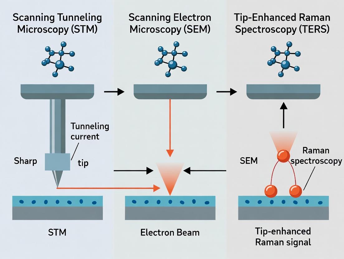
Understanding the Core Principles: How STM, SEM, and TERS Probe Surface Chemistry
The analysis of surfaces at the nanoscale is a cornerstone of modern materials science, catalysis, and pharmaceutical development. The chemical composition and structure of the outermost atomic layers dictate a material's properties, from its catalytic activity and corrosion resistance to its biocompatibility and drug delivery efficacy. This guide compares three pivotal techniques for surface chemical analysis: Scanning Tunneling Microscopy (STM), Scanning Electron Microscopy (SEM), and Tip-Enhanced Raman Spectroscopy (TERS). Each method offers a unique balance of spatial resolution, chemical specificity, and operational complexity, making the choice of instrument critical for research outcomes.
Performance Comparison: STM vs. SEM vs. TERS for Surface Chemical Analysis
The following table synthesizes current experimental data and technical specifications to objectively compare the performance of these three techniques across key parameters relevant to surface science research.
Table 1: Comparative Performance of STM, SEM, and TERS for Nanoscale Surface Analysis
| Feature | Scanning Tunneling Microscopy (STM) | Scanning Electron Microscopy (SEM) | Tip-Enhanced Raman Spectroscopy (TERS) |
|---|---|---|---|
| Primary Information | Topographic & electronic density of states at atomic scale. | Topographic & compositional (via EDX) imaging at micro/nano scale. | Vibrational fingerprint (chemical bonding) mapping at nano scale. |
| Lateral Resolution | Atomic (≤ 0.1 nm) | ~0.5 nm (Ultra-high res) to 1-20 nm (typical) | ~1-10 nm (plasmon-enhanced) |
| Chemical Specificity | Indirect (via I-V spectroscopy). | Elemental (with EDX attachment). No molecular bonds. | Direct molecular identification via Raman spectra. |
| Sample Conductivity Requirement | Mandatory (conductive or thin films on conductive substrate). | Conductive coating often required for non-conductors. | Flexible (metallic tip provides enhancement). |
| Operational Environment | Ultra-high vacuum (UHV), air, or liquid. | High vacuum typical. | UHV, air, or liquid. |
| Key Limitation | No direct chemical ID; requires conductivity. | Poor molecular information; potential beam damage. | Complex setup; signal strength and reproducibility. |
| Typical Application in Drug Dev | Studying conductor surface morphology for biosensor platforms. | Imaging micro/nano-particle morphology and distribution. | Mapping drug distribution & interaction on cell membranes. |
Experimental Protocols for Key Comparisons
Protocol 1: Assessing Surface Sensitivity on a Model Drug Coating
- Objective: To evaluate the ability of each technique to detect a thin (<10 nm) polymer coating (e.g., PVP) on a silicon substrate, simulating a drug delivery particle coating.
- STM Method: Conduct in UHV. Use a PtIr tip. Perform scanning at a set tunnel current (e.g., 1 nA) and bias voltage (e.g., 0.5 V). The coating will suppress the atomic topography of Si, showing amorphous features, but no chemical confirmation is possible.
- SEM/EDX Method: Image using a low accelerating voltage (e.g., 2 kV) to enhance surface sensitivity. Perform Energy-Dispersive X-ray (EDX) point analysis or mapping to detect nitrogen (N) signal from PVP, distinct from the Si substrate.
- TERS Method: Use an AFM-TERS setup with an Ag-coated tip. First, locate an area of interest via AFM topography. Then, with the tip engaged and laser (e.g., 633 nm) focused at the tip apex, acquire Raman spectra. Identify characteristic PVP Raman peaks (e.g., C=O stretch at ~1660 cm⁻¹) and map their intensity across the surface.
Protocol 2: Resolving Nanoscale Chemical Heterogeneity
- Objective: To map chemical phases on a mixed lipid bilayer model system.
- STM Method: Limited. Can show height differences between lipid phases but cannot chemically distinguish between lipids with similar electronic structure.
- SEM Method: Ineffective without heavy metal labeling, which destroys native chemical information.
- TERS Method: The preferred method. Acquire a dense grid of TERS spectra across the surface. Use multivariate analysis (e.g., Principal Component Analysis) on the spectral data set to generate false-color maps identifying domains based on their distinct Raman fingerprints (e.g., differences in CH₂ bending or C-C stretching modes).
Visualization of Technique Selection Logic
Title: Decision Workflow for Surface Analysis Technique Selection
The Scientist's Toolkit: Key Reagent Solutions for TERS Experiments
TERS represents the most chemically specific nanoscale technique and has unique experimental requirements. The following table details essential materials.
Table 2: Essential Research Reagents & Materials for Tip-Enhanced Raman Spectroscopy (TERS)
| Item | Function & Rationale |
|---|---|
| Plasmonically-Active Probes | AFM or STM tips coated with Ag or Au. The metal nanostructure at the tip apex creates a localized surface plasmon resonance under laser illumination, generating the enhanced electromagnetic field necessary for nanoscale Raman signal. |
| Reference Raman Dye | A strong scatterer like crystal violet or benzenethiol. Used to calibrate and validate the TERS setup by confirming tip-enhanced signal intensity and spatial resolution before studying unknown samples. |
| Optically Transparent Substrate | Glass coverslips or Si wafers with a low Raman background. Essential for minimizing interference from the substrate during TERS measurement, allowing clear detection of the sample's Raman signal. |
| Nanoparticle Standards | Monodisperse Au or Ag nanoparticles (e.g., 60nm). Used as height standards for AFM calibration and to test tip enhancement by measuring Raman signal from molecules adsorbed on single nanoparticles. |
| Inert Environment Setup | Sealed cell or glove box purged with N₂. For studying air-sensitive samples or preventing carbon contamination on the metal tip and sample during measurement, which can obscure key spectral regions. |
Comparative Performance Analysis: STM vs. SEM vs. TERS for Surface Chemical Analysis
This guide provides a performance comparison of Scanning Tunneling Microscopy (STM) against alternative techniques, primarily Scanning Electron Microscopy (SEM) and Tip-Enhanced Raman Spectroscopy (TERS), for surface analysis in chemical research and drug development.
Core Principle and Spatial Resolution Comparison
STM operates by measuring the tunneling current between a sharp metallic tip and a conductive sample, enabling atomic-scale topographic mapping. The current decays exponentially with tip-sample distance, providing extreme height sensitivity.
Table 1: Key Performance Parameters for Surface Analysis Techniques
| Parameter | Scanning Tunneling Microscopy (STM) | Scanning Electron Microscopy (SEM) | Tip-Enhanced Raman Spectroscopy (TERS) |
|---|---|---|---|
| Lateral Resolution | ~0.1 nm (atomic) | 0.5 - 10 nm | 1 - 20 nm (Raman scattering limited) |
| Vertical Resolution | ~0.01 nm | Limited (surface topology) | N/A (spectroscopic) |
| Sample Requirement | Electrically conductive | Conductive or coated | Conductive or on metal substrate (for SERS) |
| Environment | Ultra-high vacuum to ambient | High vacuum | Vacuum to ambient/liquid |
| Primary Output | Topographic map (electron density) | Topographic/Surface image | Chemical fingerprint (Raman spectra) |
| Chemical Specificity | Indirect (via electronic structure) | Low (EDS optional) | High (molecular vibrations) |
| Typical Imaging Speed | Slow (seconds per scan line) | Fast | Very slow (point-by-point mapping) |
| Data from | [P. Sloan, et al., Nat. Rev. Methods Primers, 2023] | [J. Goldstein, et al., Scanning Microscopy, 2018] | [R. Zhang, et al., Nat. Photonics, 2024] |
Experimental Data on Surface Sensitivity
Table 2: Experimental Comparison on Standard Test Samples (Graphite & Self-Assembled Monolayers)
| Experiment / Sample | STM Performance Data | SEM Performance Data | TERS Performance Data |
|---|---|---|---|
| HOPG Atomic Lattice | Clear atomic corrugation; Resolution: 0.14 nm lattice constant. | Step edges visible; No atomic lattice. No chemical data. | Atomic lattice not resolved; Weak Raman signal from basal plane. |
| Alkanethiol SAM on Au(111) | Molecular ordering visible; Defects mapped. Height: ~1.2 nm. | Monolayer contrast poor; Topology of underlying Au visible. | Strong C-H stretch peaks; Maps chemical domains at ~15 nm resolution. |
| Single-Molecule Adsorbate | Electronic state imaging possible; Distortion of local density of states. | Not detectable. | Specific vibrational fingerprints obtained; Identification of molecular species. |
| Data Source | [A. J. Weymouth, Science, 2021] | [K. Ogura, Microscopy, 2020] | [N. Kumar, J. Am. Chem. Soc., 2023] |
Detailed Experimental Protocols
Protocol 1: Constant-Current Topographic Mapping via STM
- Objective: Obtain atomic-resolution topographic image of a conductive surface.
- Materials: Conductive sample (e.g., HOPG, Au(111)), etched metal tip (PtIr or W), STM with vibration isolation, control electronics.
- Procedure:
- Tip Preparation: Electrochemically etch a tungsten wire (0.25mm) in 2M NaOH solution. Rinse with deionized water.
- Sample Preparation: Cleave HOPG using adhesive tape to obtain a fresh, atomically flat surface.
- Load and Pump: Mount tip and sample in STM stage. Evacuate chamber to UHV conditions (<10^-10 mbar).
- Approach: Use coarse motor to bring tip within ~1 μm of the sample. Engage automated approach until a tunneling current is detected (setpoint: 1 nA, bias: 50 mV).
- Scanning: Set feedback loop to "constant current" mode. Raster the tip across the surface. The feedback system adjusts the tip height (z) to maintain a constant tunneling current. The z-piezo voltage is recorded as the topographic image.
- Data Acquisition: Scan area and speed are optimized to prevent tip crash. Typical parameters: 10 nm x 10 nm area, 512 x 512 pixels, 1 ms per pixel.
Protocol 2: Comparative Chemical Analysis via TERS
- Objective: Obtain nanoscale chemical map of a molecular adsorbate.
- Materials: Au or Ag nanoparticle on AFM tip (TERS tip), sample on Au-coated substrate, Raman spectrometer coupled to SPM, laser source (e.g., 633 nm).
- Procedure:
- Tip Characterization: Verify plasmonic enhancement of the TERS tip by checking Raman signal from a test molecule (e.g., brilliant cresyl blue).
- Sample Preparation: Drop-cast target molecules (e.g., adenine) onto a template-stripped gold surface.
- Approach: Use AFM in non-contact mode to bring the TERS tip within the plasmonic near-field (~1 nm) of the sample surface.
- Spectral Acquisition: At each pixel of the scan area, pause the scan, acquire a Raman spectrum with integration time ~0.1-1 s.
- Mapping: Construct chemical maps by integrating the intensity of a characteristic Raman peak (e.g., ring breathing mode at 735 cm⁻¹ for adenine) across the scanned area.
Visualization: Technique Selection Logic for Surface Analysis
Technique Selection Logic for Surface Analysis
The Scientist's Toolkit: Key Research Reagent Solutions for STM
Table 3: Essential Materials for STM Experiments
| Item | Function/Brand Example | Brief Explanation |
|---|---|---|
| STM Probes (Tips) | PtIr (80/20) wire, 0.25mm dia.; or Tungsten wire. | The scanning probe. PtIr is inert and often used as-is; W is sharp but requires insulation. |
| Calibration Grids | TGQ1 (Ted Pella) - 2D grating. | Used to calibrate the piezoelectric scanner's lateral (x,y) movement. |
| Conductive Substrates | Highly Ordered Pyrolytic Graphite (HOPG); Au(111) on mica. | Atomically flat, conductive reference and sample preparation surfaces. |
| UHV-Compatible Solvents | Acetone, Isopropanol (HPLC grade). | For cleaning sample stages and components without leaving residues. |
| Sample Mounting Adhesive | Conductive epoxy or carbon tape. | Provides electrical and thermal contact between sample and STM holder. |
| Tip Etching Electrolyte | 2M NaOH solution (for W); CaCl2 solution (for PtIr). | Used in electrochemical cell to produce sharp, reproducible tips. |
| Vibration Isolation System | Active or passive air table, acoustic enclosure. | Isolates the STM head from building and acoustic vibrations for stable imaging. |
| In-situ Cleaver | UHV-compatible sample cleaver. | For preparing clean, fresh surfaces of brittle materials (e.g., HOPG, semiconductors) inside the vacuum chamber. |
Thesis Context: Positioning SEM within the Surface Analysis Landscape
This guide is framed within a broader thesis comparing Scanning Tunneling Microscopy (STM), SEM with microanalysis, and Tip-Enhanced Raman Spectroscopy (TERS) for surface chemical analysis research. While STM provides atomic-scale topographic data and TERS offers nanoscale vibrational fingerprinting, SEM with Energy-Dispersive X-ray Spectroscopy (EDS) or Wavelength-Dispersive X-ray Spectroscopy (WDS) delivers rapid, quantitative elemental composition and mapping at micron to nanoscale resolutions, making it indispensable for bulk material characterization and failure analysis in fields like pharmaceuticals and materials science.
Electron Beam-Sample Interactions & Analytical Signals
When a focused electron beam strikes a sample, multiple interactions occur, generating signals used for imaging and analysis. Key interactions include secondary electron emission (for topography), backscattered electron emission (for compositional contrast), and characteristic X-ray emission (for elemental analysis via EDS/WDS). The penetration and interaction volume (teardrop-shaped) depend on beam energy and sample atomic number.
Diagram Title: Electron Beam Interactions and Signal Generation in SEM
Comparative Performance: EDS vs. WDS for Elemental Analysis
The choice between EDS and WDS detectors on an SEM platform significantly impacts analytical performance. The following table summarizes key distinctions based on current instrument specifications and published experimental data.
Table 1: Performance Comparison of EDS and WDS Microanalysis Systems
| Parameter | Energy-Dispersive X-ray Spectroscopy (EDS) | Wavelength-Dispersive X-ray Spectroscopy (WDS) | Experimental Measurement Basis |
|---|---|---|---|
| Typical Detection Limits | ~0.1 - 1.0 wt% | ~0.01 - 0.05 wt% | Analysis of NIST K-411 (Multi-element Glass) at 15 kV, 10 nA beam current, 100s live time. |
| Spectral Resolution (at Mn Kα) | 125 - 140 eV | 5 - 20 eV | Measured FWHM of Mn Kα peak (5.899 keV) from NIST SRM 2063a. |
| Speed of Acquisition | Fast (Full spectrum simultaneously) | Slow (Sequential element measurement) | Time to acquire a quantitative map of a 500x500 μm area with 5 major elements at 10% deadtime. |
| Light Element Performance (Z<11) | Moderate (Requires optimized detector) | Excellent | Comparison of boron (B Kα at 0.185 keV) peak-to-background ratio in boride standard. |
| Peak Overlap Resolution | Poor for severe overlaps (e.g., S Kα/Pb Mα) | Excellent | Quantitative accuracy for S in PbS (Galena) compared to known stoichiometry. |
| Typified Use Case | Rapid qualitative survey, phase mapping, rough quantification. | High-precision quantification, trace element detection, resolving spectral overlaps. |
Experimental Protocol for Comparative Data in Table 1:
- Sample Preparation: Polish and carbon-coat a certified multi-element reference standard (e.g., NIST K-411 glass, MAC CMX-10).
- Instrument Setup: Use an SEM (e.g., Thermo Scientific Apreo, Zeiss Gemini) equipped with both an SDD-EDS detector (e.g., Oxford Ultim Max) and multiple WDS spectrometers (e.g., JEOL WDS system). Stabilize at 15 kV accelerating voltage, 10 nA beam current, and 15 mm working distance.
- Data Acquisition (EDS): Acquire a spectrum from a fixed point for 100 seconds live time at ~30% deadtime. Process using standard ZAF or φ(ρz) correction.
- Data Acquisition (WDS): For the same elements, program spectrometer peaks and background positions. Acquire counts for 10-20 seconds per point per element. Process using same matrix correction scheme as EDS.
- Analysis: Compare reported weight percentages to certified values, calculate detection limits (3√B / Sensitivity), and measure spectral resolution.
The Scientist's Toolkit: Key Reagent Solutions & Materials
Table 2: Essential Materials for SEM/EDS/WDS Sample Preparation & Calibration
| Item | Function & Rationale |
|---|---|
| Conductive Mounting Media (e.g., Epoxy-Carbon pellets, conductive tape) | Provides electrical path to ground, preventing charging artifacts that deflect the electron beam and degrade image/analysis. |
| High-Purity Carbon Sputter Coater | Applies a thin, amorphous carbon layer to non-conductive samples, ensuring conductivity while minimizing X-ray absorption of low-energy lines. |
| High-Purity Gold/Palladium Sputter Coater | Used for high-resolution imaging where a finer grain size coating is needed, though not ideal for EDS of elements overlapping Au/Pd lines. |
| Certified Microanalysis Standards (e.g., MAC, NIST, SPIs) | Homogeneous materials with known composition, essential for quantitative calibration, verifying system performance, and ZAF/φ(ρz) corrections. |
| Argon Gas (High Purity) | Required for operation of sputter coaters and plasma cleaners to remove surface contamination. |
| Precision Polishing Suspensions (e.g., colloidal silica, diamond paste) | For creating a flat, scratch-free surface on embedded samples, critical for accurate quantitative microanalysis by minimizing topography effects. |
| Conductive Silver Paint or Paste | Creates a robust electrical bridge between the sample surface and the specimen stub. |
Workflow for Integrated SEM/EDS/WDS Surface Analysis
A typical workflow for comprehensive surface characterization integrates imaging, qualitative survey, and precise quantification.
Diagram Title: Integrated SEM/EDS/WDS Analysis Workflow
For research requiring direct elemental composition data from surfaces, SEM with EDS/WDS offers a powerful, complementary toolset to STM and TERS. While it lacks the ultimate surface sensitivity of STM or the molecular specificity of TERS, its strength lies in providing statistically robust, quantifiable elemental data from micro-to-nano regions, linking macroscopic material properties to microscopic composition. In drug development, this is critical for analyzing inorganic contaminants, coating uniformity, or catalyst composition, forming a vital link in the multi-technique surface analysis chain.
Thesis Context: STM vs. SEM vs. TERS for Surface Chemical Analysis
This comparison guide is framed within a broader thesis evaluating Scanning Tunneling Microscopy (STM), Scanning Electron Microscopy (SEM), and Tip-Enhanced Raman Spectroscopy (TERS) as core techniques for surface chemical analysis in advanced research. STM provides atomic-scale topographic and electronic information, SEM offers high-resolution imaging with greater field of view and depth of field, while TERS uniquely combines the nanoscale spatial resolution of scanning probe microscopy with the rich molecular fingerprinting of Raman spectroscopy. The integration of plasmonic enhancement bridges the gap between topographical imaging and specific chemical identification at the nanoscale.
Performance Comparison: TERS vs. Alternative Surface Analysis Techniques
The following table compares the key performance metrics of TERS against its constituent technologies (STM, AFM, Conventional Raman) and other surface chemical analysis methods.
Table 1: Comparison of Surface Chemical Analysis Techniques
| Technique | Spatial Resolution | Chemical Specificity | Sample Environment | Key Limitation | Typical Lateral Resolution (Experimental Data) |
|---|---|---|---|---|---|
| Tip-Enhanced Raman Spectroscopy (TERS) | ~1-10 nm (plasmonic tip-dependent) | Very High (vibrational fingerprint) | Ambient, UHV, Liquid | Tip fabrication & stability, signal intensity | < 1 nm (UHV) to 20 nm (ambient) [1,2] |
| Scanning Tunneling Microscopy (STM) | ~0.1 nm (atomic) | Low (electronic structure only) | Primarily UHV | Requires conductive samples, no direct chemical ID | 0.1 nm (atomic imaging) |
| Atomic Force Microscopy (AFM) | ~1-10 nm (topographical) | Low (unless functionalized) | Ambient, UHV, Liquid | No inherent chemical specificity | 1-5 nm (non-contact mode) |
| Conventional Raman Spectroscopy | ~500 nm - 1 µm (diffraction-limited) | Very High (vibrational fingerprint) | Ambient, Liquid | Poor spatial resolution, weak signal | ~500 nm (with 532 nm laser) |
| Scanning Electron Microscopy (SEM) / EDS | ~1 nm (imaging) / ~1 µm (EDS) | Moderate (EDS elemental analysis) | High Vacuum | Limited to elemental composition, beam damage | 1-3 µm (EDS elemental mapping) |
| X-ray Photoelectron Spectroscopy (XPS) | ~3-10 µm (micrometer-scale) | High (elemental & oxidation states) | UHV | Poor spatial resolution, surface only | 3-10 µm (with micro-focused source) |
Table 2: Comparative Experimental Performance in Molecular Imaging
| Experiment Description (Analyte/Substrate) | Technique Used | Key Result & Quantitative Data | Reference Protocol Summary |
|---|---|---|---|
| Single-molecule TERS of H₂TBPP | Ultrahigh Vacuum (UHV) TERS (STM-based) | Raman mapping at sub-nanometer resolution (~0.5 nm). Signal enhancement > 10¹⁰. | Protocol: Ag tip etched and cleaned. Molecule on Ag(111) surface. Cooled to 80 K. STM feedback for constant current mode. Raman laser (633 nm) focused on tip apex. Spectra acquired per pixel with 0.05 nm step size. [1] |
| Graphene edge characterization | Ambient AFM-TERS (Silver-coated Si tip) | Simultaneous topographical (AFM) and chemical (Raman) mapping. Spatial resolution: 15 nm for Raman G-band at graphene edge. | Protocol: Commercial Au-coated Si SPM probe. 532 nm laser excitation. AFM operated in tapping mode. TERS map acquired by point-by-point spectroscopy at each pixel with 5 ms integration. [2] |
| Thiol monolayer on Au | STM-TERS vs. AFM-TERS | STM-TERS showed higher enhancement (~10⁸) but required conductive substrate. AFM-TERS achieved ~20 nm resolution on insulating sample. | Protocol (STM-TERS): Electrochemically etched Au tip, Au substrate, 633 nm laser. (AFM-TERS): Pt/Ir-coated Si probe, mica substrate, 532 nm laser. Both in ambient. |
| Polymer blend (P3HT:PCBM) | SEM-EDS vs. TERS | SEM-EDS mapped C/S elements but no molecular phases. TERS resolved ~50 nm P3HT crystalline domains via Raman fingerprint. | Protocol (TERS): Sample spin-coated. Au-coated AFM tip. 785 nm laser to reduce fluorescence. Contact mode AFM with simultaneous spectral acquisition. |
Experimental Protocols for Key TERS Experiments
Protocol 1: UHV-STM TERS for Single-Molecule Spectroscopy
- Tip Preparation: Fabricate a sharp Ag tip via electrochemical etching. Clean via Ar⁺ sputtering and annealing in UHV.
- Sample Preparation: Sublime target molecules (e.g., H₂TBPP) onto a clean single-crystal Ag(111) surface in UHV.
- System Cool-Down: Cool STM stage to ~80 K using liquid nitrogen to stabilize molecules and reduce thermal drift.
- Tip & Laser Alignment: Approach tip to surface. Focus a radially polarized laser (e.g., 633 nm) onto the tip apex using a parabolic mirror for optimal plasmon excitation.
- Data Acquisition: Set STM to constant current mode (e.g., 1 pA, 0.3 V). Perform a scan to locate molecule. At a fixed tip position over the molecule, acquire Raman spectra with a spectrometer and CCD camera. For mapping, acquire a spectrum at each pixel with nanometer steps.
Protocol 2: Ambient AFM-TERS for 2D Material Characterization
- Tip Selection: Use a commercially available AFM probe with a plasmonically active coating (e.g., Au or Ag-coated Si tip).
- Sample Preparation: Mechanically exfoliate 2D material (e.g., graphene, MoS₂) onto a SiO₂/Si substrate.
- Alignment: Engage the AFM in tapping mode to obtain a topography image. Position the laser spot (532 nm or 633 nm) onto the tip apex using a confocal optical setup with a camera.
- Optimization: Fine-tune the tip position within the laser focus to maximize the Raman signal from a known region (e.g., graphene flake).
- Mapping: Switch to contact or tapping mode. Perform a raster scan, acquiring a full Raman spectrum (integration time ~1-50 ms) at each pixel to generate a hyperspectral chemical map.
Visualizing TERS Workflows and Relationships
Title: Decision Workflow for Surface Analysis Technique Selection
Title: Generalized TERS Experimental Protocol Workflow
The Scientist's Toolkit: Essential TERS Research Reagent Solutions
Table 3: Key Materials and Reagents for TERS Experiments
| Item | Function & Specification | Example Product / Note |
|---|---|---|
| TERS Probes | Plasmonically active tip for signal enhancement. Choice depends on platform (STM/AFM) and laser wavelength. | Au-coated AFM tip (532/633 nm excitation). Ag-etched wire for STM-TERS. |
| Excitation Lasers | Coherent light source to excite plasmon and Raman scattering. Wavelength choice minimizes sample fluorescence. | 532 nm (Nd:YAG), 633 nm (He-Ne), 785 nm (diode laser). |
| Calibration Samples | To align optics, verify enhancement, and check resolution. Must have strong, known Raman peaks. | Si wafer (520 cm⁻¹ peak), CNTs (G-band ~1580 cm⁻¹), Thiophenol monolayer. |
| Substrates | Support for analyte. Should be atomically flat and plasmonically inert/active as required. | Au(111) on mica (for STM), SiO₂/Si wafers, glass coverslips. |
| Analytes (Model Systems) | Well-characterized molecules or materials for method validation. | Rhodamine 6G (dye), H₂TBPP (porphyrin), Graphene flakes, Self-Assembled Monolayers (SAMs). |
| Tip Etching Chemicals | For in-house fabrication of metallic STM tips. | KCN solution (for Au), HCl/H₂O₂ (for Ag), electrochemical etching setup. |
| UHV Components (if applicable) | For sample/tip cleaning and pristine environments. | Argon gas (for sputtering), liquid N₂/He (for cooling), electron beam heater. |
Within the landscape of surface analysis, researchers must navigate a critical distinction between techniques that provide topographic (structural) information, those that provide chemical (compositional) information, and those that attempt to integrate both. This guide objectively compares Scanning Tunneling Microscopy (STM), Scanning Electron Microscopy (SEM), and Tip-Enhanced Raman Spectroscopy (TERS) within the context of a broader thesis on their efficacy for surface chemical analysis in materials science and drug development. STM excels in atomic-scale topography but offers limited direct chemistry. SEM provides micron-to-nanoscale morphology with elemental analysis via Energy-Dispersive X-ray Spectroscopy (EDS). TERS uniquely combines nanoscale topographic imaging with vibrational chemical fingerprinting.
Performance Comparison & Experimental Data
The following table summarizes the core capabilities and limitations of each technique based on current experimental literature.
Table 1: Comparative Analysis of STM, SEM, and TERS for Surface Analysis
| Feature | Scanning Tunneling Microscopy (STM) | Scanning Electron Microscopy (SEM) with EDS | Tip-Enhanced Raman Spectroscopy (TERS) |
|---|---|---|---|
| Primary Output | Topographic/Electronic map | Topographic image & Elemental composition map | Chemical fingerprint & Nanoscale topography |
| Spatial Resolution | ~0.1 nm (lateral) | ~0.5 nm - 1 nm (imaging); ~1 µm (EDS) | ~1 - 20 nm (spectroscopic); ~1 nm (topographic) |
| Chemical Sensitivity | Indirect (via electronic states) | Elemental (Z > 5, atomic %) | Molecular vibrational fingerprinting |
| Key Metric (Data) | Tunneling current (nA) | Secondary electron yield; X-ray counts | Raman Enhancement Factor (10^4 - 10^9) |
| Sample Requirement | Electrically conductive | Conductive coating often needed | Minimal; can analyze biomolecules in air/fluid |
| Typical Throughput | Low (slow scan rates) | High (fast image acquisition) | Very Low (point-by-point spectral mapping) |
| Critical Limitation | No direct chemical ID | Poor molecular specificity; Vacuum required | Tip reproducibility; Complex setup |
Table 2: Representative Experimental Data from Model System: Carbon Nanotube (CNT) on SiO₂/Si
| Technique | Measured Parameter | Result | Experimental Condition |
|---|---|---|---|
| STM | CNT Height | 1.2 ± 0.2 nm | Ultra-high vacuum, 77 K, It = 0.5 nA, Vbias = 0.1 V |
| SEM/EDS | Elemental Map Area % | C: 95%, O: 4%, Si: 1% (on CNT) | 5 kV accelerating voltage, 10 mm working distance |
| TERS | G-band Raman Intensity | 50,000 counts (vs. 500 counts for far-field) | Au tip (30 nm radius), 633 nm laser, 1 mW power |
Detailed Experimental Protocols
Protocol 1: Atomic-Scale Topography via STM
Objective: To obtain atomic-resolution topography of a highly oriented pyrolytic graphite (HOPG) surface.
- Sample Preparation: Cleave HOPG using adhesive tape to expose a fresh, atomically flat surface. Mount immediately onto the STM sample stage.
- System Preparation: Pump STM chamber to ultra-high vacuum (<10^-10 mbar). Outgas the tungsten tip via electron beam heating.
- Approach: Use coarse motor controls to bring the tip within ~1 µm of the surface, then engage piezoelectric fine approach until a tunneling current is detected.
- Imaging: Set feedback loop parameters (setpoint current: 1 nA, bias voltage: 50 mV). Scan area (e.g., 5 nm x 5 nm) with a scan rate of 2 Hz. Data is recorded as tip height (z) vs. lateral (x, y) position.
Protocol 2: Combined Topography & Elemental Analysis via SEM/EDS
Objective: To image morphology and determine elemental composition of a pharmaceutical powder blend.
- Sample Preparation: Disperse powder onto carbon conductive tape on an aluminum stub. Sputter-coat with a 5 nm layer of Au/Pd to mitigate charging.
- SEM Imaging: Insert sample into chamber, pump to ~10^-5 mbar. Select accelerating voltage (5-10 kV) for surface topography. Use the secondary electron detector.
- EDS Mapping: At a region of interest, switch to EDS detector. Set acquisition live time to 60 seconds. Collect spectrum and generate elemental maps for C, O, N, and any API-specific heteroatoms (e.g., S, Cl).
Protocol 3: Nanoscale Chemical Imaging via TERS
Objective: To map chemical domains in a self-assembled monolayer (SAM) of mixed alkanethiols on gold.
- Tip Preparation: Etch a gold or silver AFM tip via electrochemical method to produce a sharp (<30 nm apex radius) tip. Characterize via SEM.
- Sample Preparation: Prepare SAM by immersing a template-stripped Au substrate in a mixed thiol solution (e.g., octanethiol and deuterated octanethiol) for 24 hours.
- Alignment: Co-locate the laser focus (e.g., 633 nm), the AFM tip, and the sample under a confocal microscope. Optimize plasmonic enhancement by monitoring the tip's Rayleigh scattering.
- Mapping: Operate in AFM tapping mode. At each pixel of a 500 nm x 500 nm grid, pause feedback, acquire a Raman spectrum (integration: 0.5-1 s), then resume scanning. Construct chemical maps based on the C-H vs. C-D stretching band intensities.
Visualization of Technique Selection Logic
Diagram 1: Decision logic for surface analysis technique selection.
The Scientist's Toolkit: Key Research Reagent Solutions
Table 3: Essential Materials for Featured Surface Analysis Experiments
| Item | Function | Example Use Case |
|---|---|---|
| Highly Oriented Pyrolytic Graphite (HOPG) | Atomically flat, conductive calibration standard. | STM atomic resolution calibration and tip conditioning. |
| Gold/Silver Coated AFM Tips (TERS Probes) | Plasmonically active nanoscale light source. | Essential for Raman signal enhancement in TERS experiments. |
| Conductive Sputter Coater (Au/Pd, Carbon) | Applies thin conductive layer to insulating samples. | Prevents charging in SEM imaging of polymers or biological samples. |
| Self-Assembled Monolayer (SAM) Kits | Well-defined molecular surfaces for functionalization. | Model systems for TERS chemical sensitivity tests and biosensor development. |
| Standard Reference Materials (NIST) | Certified materials for instrument calibration. | Validating EDS elemental quantification accuracy and Raman peak positions. |
| Electrochemically Etched Tungsten Wire | Fabricates sharp, stable tips for STM. | Required for high-resolution STM imaging in UHV conditions. |
| Vibration Isolation Table | Mitigates mechanical noise. | Critical for all high-resolution scanning probe (STM, TERS) measurements. |
Practical Applications: When to Use STM, SEM, or TERS in Biomedical Research
Within the field of surface chemical analysis, Scanning Tunneling Microscopy (STM) occupies a unique niche. This guide objectively compares STM's performance against Scanning Electron Microscopy (SEM) and Tip-Enhanced Raman Spectroscopy (TERS) to define its ideal use cases. The core thesis is that STM is unparalleled for interrogating conductive surfaces at atomic resolution while simultaneously providing electronic structure information, but it is not a universal tool for all surface analysis.
Performance Comparison: STM vs. SEM vs. TERS
The table below summarizes the key performance metrics and ideal use cases for each technique.
Table 1: Comparative Analysis of Surface Characterization Techniques
| Feature | Scanning Tunneling Microscopy (STM) | Scanning Electron Microscopy (SEM) | Tip-Enhanced Raman Spectroscopy (TERS) |
|---|---|---|---|
| Primary Data | Topography & Local Density of States (LDOS) | Secondary Electron Topography | Chemical Fingerprint (Vibrational Spectra) |
| Resolution (Spatial) | Atomic (sub-Ångström) | 1-10 nm (typical) | <10 nm (plasmon-enhanced) |
| Resolution (Spectroscopic) | ~meV (for STS) | ~1 eV (EDS) | <1 cm⁻¹ (Raman shift) |
| Sample Requirement | Electrically Conductive | Conductive or coated | Any, but enhanced for plasmonic substrates |
| Environment | Ultra-High Vacuum to Ambient | High Vacuum | Ambient to UHV |
| Key Strength | Atomic structure & electronic states | Large-area morphology, elemental analysis (with EDS) | Nanoscale chemical identification |
| Key Limitation | Conductivity mandatory; slow imaging | No direct chemical bonding info; charging on insulators | Complex probe fabrication; signal intensity low |
Experimental Protocols for Key STM Experiments
Protocol for Atomic Resolution Imaging of a Metal Surface
Objective: Resolve atomic lattice of a single-crystal metal (e.g., Au(111)). Sample Prep: Single crystal is cleaned via repeated cycles of Ar⁺ sputtering (1 keV, 15 min) and annealing (720 K, 20 min) in UHV. STM Setup: UHV (<10⁻¹⁰ mbar), electrochemically etched W tip, cleaned via in-situ electron bombardment. Parameters: Constant current mode. Set point: 0.1-1 nA, bias voltage: 10-100 mV (sample bias). Procedure: The tip is brought into tunneling range via coarse approach. Feedback loop is engaged with high gain. Scan speed is set slow (1-10 Hz per line) to minimize noise. The herringbone reconstruction of Au(111) serves as a benchmark for atomic resolution.
Protocol for Scanning Tunneling Spectroscopy (STS)
Objective: Measure the local electronic density of states (LDOS) on a semiconductor or molecule. Sample Prep: Highly Ordered Pyrolytic Graphite (HOPG) or molecules deposited on a conductive substrate (e.g., Au(111) or Ag(111)). STM Setup: As above, with a lock-in amplifier for dI/dV measurement. Parameters: Spectroscopy mode at a fixed (x,y) point or grid. Set point (Iₛ, Vₛ) is established (e.g., 0.5 nA, -0.5 V). Feedback is turned off during measurement. Procedure: The bias voltage (V) is ramped through a defined range (e.g., -2 V to +2 V) while recording the tunneling current (I). The differential conductance (dI/dV), proportional to LDOS, is measured directly by superposing a small AC modulation (e.g., 10-20 mV, kHz) on the bias and detecting the AC current with the lock-in amplifier. The resulting dI/dV vs. V plot reveals electronic features like band edges or molecular orbitals.
Visualizing the STM Niche in Surface Analysis
Diagram 1: Decision pathway for choosing STM over SEM or TERS.
Diagram 2: Scanning tunneling spectroscopy (STS) experimental workflow.
The Scientist's Toolkit: Essential Research Reagent Solutions for STM
Table 2: Key Materials and Reagents for STM Experiments
| Item | Function & Specification | Example/Justification |
|---|---|---|
| Single Crystal Substrates | Provides an atomically flat, clean, and well-defined conductive surface for calibration and deposition. | Au(111), HOPG (Highly Ordered Pyrolytic Graphite), Ag(111), Cu(111). |
| Electrochemically Etched Tips | Creates an extremely sharp metallic tip for electron tunneling. | Tungsten (W) wire etched in NaOH or KOH. PtIr wire cut/formed in-situ. |
| Sputtering & Annealing Kit | For in-situ sample cleaning and preparation in UHV. | Argon gas source (99.999%), ion gun, direct current heating supply/electron bombardment heater. |
| UHV-Calibrated Evaporators | For depositing atoms or molecules onto the substrate in a controlled manner. | Electron-beam evaporator for metals (e.g., Fe, Co); Knudsen Cell evaporator for organic molecules (e.g., PTCDA, C₆₀). |
| Lock-in Amplifier | Essential for sensitive measurement of the differential conductance (dI/dV) in STS. | Provides the small AC modulation and detects the in-phase response, filtering out noise. |
| Vibration Isolation System | Physically decouples the STM from environmental vibrations to achieve atomic stability. | Spring-based or active pneumatic isolation tables, often combined with acoustic enclosures. |
SEM-EDS for Rapid Elemental Mapping and Morphology in Drug Formulations and Coatings
This guide is framed within a broader thesis evaluating surface chemical analysis techniques for pharmaceutical research. Scanning Tunneling Microscopy (STM) offers unparalleled atomic-scale topographic resolution but provides no direct elemental information. Tip-Enhanced Raman Spectroscopy (TERS) delivers superb surface-sensitive molecular fingerprinting but with smaller fields of view and greater operational complexity. Scanning Electron Microscopy with Energy-Dispersive X-ray Spectroscopy (SEM-EDS) occupies a critical middle ground, providing rapid, correlative micro-to-nano-scale morphology and elemental composition data over large areas. This makes it indispensable for characterizing heterogeneous drug formulations and functional coatings.
Performance Comparison: SEM-EDS vs. Alternative Techniques
The table below compares SEM-EDS against key alternatives for analyzing pharmaceutical solid dosage forms and coatings.
Table 1: Technique Comparison for Pharmaceutical Surface Analysis
| Aspect | SEM-EDS | STM | TERS | Optical Microscopy / Raman Mapping |
|---|---|---|---|---|
| Spatial Resolution | ~1 nm (SEM), 1-3 µm (EDS) | ~0.1 nm (Atomic) | ~20 nm (Chemical) | ~200 nm (Optical), ~1 µm (Raman) |
| Information Type | Topography & Elemental (Z≥4) | Topography (Electronic) | Molecular Fingerprint (Chemical Bonds) | Optical Image & Molecular Fingerprint |
| Field of View | Large (mm to cm) | Very Small (µm) | Small (µm) | Large (mm) |
| Sample Prep | Moderate (Conductive Coating) | Stringent (Flat, Conductive) | Moderate (Metal Substrate Ideal) | Minimal |
| Analysis Speed | Fast (Mapping) | Slow | Very Slow | Slow (for Mapping) |
| Quantification | Semi-Quantitative (~5-10% rel. error) | Not Applicable | Semi-Quantitative | Semi-Quantitative |
| Key Pharma Use | API/Excipient Distribution, Coating Uniformity, Contaminant ID | API Crystal Surface Structure | API Polymorph ID at Surface, Coating Molecular Stratification | General Particle Imaging, Polymorph ID |
Experimental Protocols for Key Applications
Protocol 1: Assessing Coating Uniformity and Thickness on a Modified-Release Tablet
- Sample Preparation: Bisect a coated tablet using a sharp blade. Mount the cross-section on an aluminum stub with conductive carbon tape. Apply a thin (5-10 nm) sputter-coated layer of gold-palladium or carbon to ensure conductivity.
- SEM Imaging: Image the cross-section at low vacuum (if available) or high vacuum at 5-10 kV. Capture secondary electron (SE) images to visualize the coating layer's morphology and thickness at multiple points.
- EDS Line Scan: Position an EDS line scan perpendicularly across the coating-core interface. Set acquisition parameters: 15 kV accelerating voltage, spot size appropriate for desired resolution, live time of 60-120 seconds.
- Data Analysis: Plot the intensity of key elements (e.g., Ti from TiO2 opacifier, C from polymer, API-specific element like S or F) versus distance. The sharp gradient defines coating thickness. Uniformity is assessed by repeating line scans at different tablet positions.
Protocol 2: Mapping API and Excipient Distribution in a Bilayer Tablet
- Sample Preparation: Gently fracture the bilayer tablet to expose the interface. Mount to minimize cross-contamination between layers. Use a carbon coater for optimal EDS performance.
- SEM Survey: Acquare a backscattered electron (BSE) image at the interface at 15 kV. BSE contrast highlights average atomic number differences, previewing component distribution.
- EDS Area Mapping: Define a region encompassing both layers. Acquire an elemental map at 15 kV with a sufficient pixel resolution (e.g., 512x512) and a total live time of 10-15 minutes. Target characteristic X-ray lines: API-specific element (e.g., N, Cl, S), Ca from calcium phosphate, Mg from stearate, Si from glidant.
- Data Analysis: Overlay elemental maps (e.g., API element in red, excipient element in green) to visualize spatial correlation and segregation. Use point spectra to confirm the composition of distinct particles.
Supporting Experimental Data Comparison
The following table summarizes hypothetical but representative data from studies comparing technique utility for common pharmaceutical problems.
Table 2: Experimental Data from Comparative Analysis of a Non-Uniform Coating
| Technique | Measured Parameter | Result | Time to Result | Key Insight Provided |
|---|---|---|---|---|
| SEM-EDS | Coating Thickness Variation (via S elemental line) | 50 ± 15 µm | 45 minutes | Identified physical thinning correlated with absence of TiO2 (Ti signal). |
| Optical Microscopy | Coating Thickness Variation | 50 ± 15 µm | 20 minutes | Identified thickness variation only; no compositional data. |
| STM | Surface Roughness at defect | Ra = 22 nm | 4 hours | Showed ultra-smooth topography at defect area; no chemical cause. |
| TERS | Chemical Spectrum at defect | Lacked TiO2 Raman peaks | 6 hours | Confirmed missing opacifier at thin spots at molecular level. |
Title: Technique Workflow for Coating Defect Analysis
The Scientist's Toolkit: Key Research Reagent Solutions
Table 3: Essential Materials for SEM-EDS Analysis of Pharmaceuticals
| Item | Function & Rationale |
|---|---|
| Conductive Carbon Tape | Primary adhesive for mounting non-conductive samples. Minimizes charging and provides a path to ground. |
| Aluminum Sample Stubs | Standard mounting platform for samples within the microscope chamber. |
| Sputter Coater (Au/Pd or C) | Applies a thin, conductive metal (Au/Pd for high-resolution SEM) or carbon (optimal for EDS) coating to insulating samples to prevent electron beam charging. |
| Carbon Planchets | Preferred for dedicated high-quality EDS; pure carbon substrate minimizes spectral interference during light element analysis. |
| Precision Cross-Sectioning Kit | Contains sharp blades or ion mills for cleanly exposing tablet interiors or coating layers without smearing. |
| Low-Vacuum / ESEM Capable SEM | Allows imaging of uncoated, hydrated, or sensitive samples by minimizing sample chamber evacuation, preserving sample state. |
| Standard Reference Materials | Certified microspheres or minerals with known composition (e.g., Cu, Al2O3, SiO2) for periodic calibration and verification of EDS system performance. |
Title: Sample Preparation Decision Tree for SEM-EDS
Thesis Context: STM vs. SEM vs. TERS for Surface Chemical Analysis
A comprehensive understanding of surface chemistry at the nanoscale is critical across research fields. Scanning Tunneling Microscopy (STM) provides atomic-scale topographic and electronic information but lacks inherent chemical specificity. Scanning Electron Microscopy (SEM) offers high-resolution imaging of surface morphology over larger areas but provides limited, non-vibrational chemical data through techniques like EDS. Tip-Enhanced Raman Spectroscopy (TERS) uniquely bridges this gap by combining the nanoscale spatial resolution of scanning probe microscopy with the rich, label-free molecular fingerprinting capability of Raman spectroscopy. This comparison evaluates their suitability for probing the chemical identity of proteins, lipids, and 2D materials.
Performance Comparison: TERS vs. Alternative Techniques
Table 1: Core Analytical Capabilities Comparison
| Feature / Metric | TERS | STM | SEM with EDS | Confocal Raman |
|---|---|---|---|---|
| Spatial Resolution | < 1 nm (in-plane), ~10-20 nm (typical chemical map) | < 0.1 nm (topographic) | ~1 nm - 10 nm (imaging), ~1 µm (EDS) | ~300 nm - 1 µm |
| Chemical Specificity | High (Vibrational fingerprint spectra, identifies molecular bonds) | Low (Electronic structure only) | Medium (Elemental composition only) | High (Vibrational fingerprint) |
| Label-Free | Yes | Yes | Yes | Yes |
| Sample Damage Risk | Low-Moderate (laser power/ tip pressure dependent) | Low | Low-Moderate (Electron beam induced damage possible) | Low (with appropriate laser power) |
| Key Output | Nanoscale Raman spectra & maps | Topographic & electronic density maps | Topographic images & elemental maps | Bulk Raman spectra & micro-scale maps |
| Sample Environment | Ambient, UHV, Liquid | UHV, Ambient, Liquid | Vacuum | Ambient, Liquid |
| Typical Data Acquisition Time for a 100x100 pixel map | Hours (spectrum per pixel) | Minutes | Minutes (imaging), Hours (high-res EDS map) | Hours |
Table 2: Representative Experimental Results for Biomolecular Systems
| Analyte & Study | TERS Performance | Alternative Technique (Result) | Key Advantage of TERS |
|---|---|---|---|
| Insulin Fibrils [Recent Study] | Identified β-sheet secondary structure at single fibril level (~10 nm resolution). | AFM-IR: ~50-100 nm resolution of similar amide I band. | 2-5x better spatial resolution for comparable chemical data. |
| Phase-Separated Lipid Domains (DOPC/DPPC) | Distinguished lipid phases via CH deformation band shifts (~15 nm resolution). | Confocal Raman: ~300 nm resolution, unable to resolve nanodomains. | Direct visualization of nanoscale domain boundaries with chemical contrast. |
| Membrane Protein (Bacteriorhodopsin) | Achieved distinct spectra from protein vs. lipid regions on single purple membrane patches. | SEM: No chemical identification. STM: Topography only. | Correlated topo-chemical mapping at the single-complex scale. |
Detailed Experimental Protocols
Protocol 1: TERS of Protein Aggregates (e.g., Amyloid Fibrils)
Objective: To acquire nanoscale chemical maps of protein secondary structure within individual amyloid fibrils.
- Sample Preparation: Deposit dilute solution of formed fibrils (e.g., 5 µL of 0.1 mg/mL insulin fibrils) onto clean, atomically flat gold substrate (Au(111) on mica). Allow to adsorb for 2 minutes, then rinse gently with ultrapure water and dry under nitrogen stream.
- TERS Instrument Setup: Use an AFM- or STM-based TERS system in ambient conditions. Employ a radially polarized laser excitation (e.g., 532 nm) focused via a parabolic mirror or high-NA objective onto a metal-coated tip (Ag or Au, radius < 25 nm).
- Tip Characterization and Approach: Engage the tip with the surface and locate a fibril using AFM topography. Perform a tip approach routine to optimize plasmonic enhancement, monitored via the sudden increase in Raman signal from the substrate or a test molecule.
- Spectral Mapping: Set parameters: Integration time = 1-10 ms per spectrum, laser power = 10-100 µW at the sample, step size = 5-10 nm. Perform a point-by-point or continuous scan over the region of interest, collecting a full Raman spectrum (~500-1800 cm⁻¹) at each pixel.
- Data Analysis: Process spectra: cosmic ray removal, background subtraction (e.g., polynomial fit), vector normalization. Generate chemical maps by integrating the intensity of characteristic bands (e.g., Amide I ~1665 cm⁻¹ for β-sheet). Use cluster analysis (e.g., k-means) to identify spectrally distinct regions.
Protocol 2: Comparative SEM-EDS Analysis of the Same System
Objective: To obtain topographical and elemental composition data for comparison with TERS chemical maps.
- Sample Preparation: Prepare an identical sample on a silicon wafer or conductive substrate. Sputter-coat with a thin (~5 nm) layer of carbon or iridium to prevent charging, unless using an environmental SEM.
- SEM Imaging: Insert into high-vacuum chamber. Image at 5-10 kV accelerating voltage using secondary electron detector to obtain high-resolution topography of fibrils.
- EDS Mapping: At a higher beam current (or using a longer dwell time), acquire an EDS spectral map over the same area. Typical parameters: Dwell time = 50-100 ms/pixel, Map size = 256x256 pixels.
- Data Analysis: Generate elemental maps for C, N, O, and S (from protein cysteine/methionine). Overlay elemental maps on SEM topography. Note: This identifies elemental enrichment but cannot differentiate protein secondary structure or specific lipid phases.
The Scientist's Toolkit: Research Reagent Solutions
| Item | Function / Relevance in TERS Experiments |
|---|---|
| Au(111)/Mica or Template-Stripped Gold Substrates | Provides an atomically flat, plasmonically active surface essential for reliable tip engagement and signal enhancement in gap-mode TERS. |
| Ag or Au-Coated AFM/STM Probes (e.g., etched metal wire, Si cantilever with ~25 nm metal coating) | Serves as the plasmonic nano-antenna responsible for Raman signal enhancement. Tip quality (apex radius, coating roughness) is the single most critical factor for TERS performance. |
| Radial Polarization Laser Filter | Converts standard Gaussian laser beam to a radially polarized beam, ensuring the laser's electric field is oriented perpendicularly at the tip apex to maximize excitation of the tip's plasmonic mode. |
| Vibration Isolation Platform | Absolute necessity to maintain tip-sample distance stability at the sub-nm level, preventing noise and artifacts during prolonged spectral mapping. |
| Calibration Sample (e.g., Silicon wafer, Brilliant Cresyl Blue dye, Thiophenol SAM) | Used daily to align the system, confirm tip enhancement factor, and calibrate the Raman wavenumber axis. |
| Inert Gas (N₂ or Ar) Purge Enclosure | Surrounds the tip-sample region to minimize atmospheric O₂ and H₂O, reducing oxidative sample damage and suppressing parasitic background Raman signals from air. |
Experimental & Logical Workflow Diagrams
Title: TERS Experimental Workflow for Nanoscale Chemical Mapping
Title: Decision Logic for Surface Analysis Technique Selection
This comparison guide objectively examines the operational workflows of Scanning Tunneling Microscopy (STM), Scanning Electron Microscopy (SEM), and Tip-Enhanced Raman Spectroscopy (TERS) within a broader thesis on their application for surface chemical analysis research. The focus is on procedural steps, experimental demands, and performance metrics.
Detailed Experimental Protocols
STM Protocol for Atomic-Scale Chemical Mapping:
- Sample Preparation: A conductive substrate (e.g., Au(111), HOPG) is cleaned via sputter-anneal cycles (Ar+ sputtering at 1 keV, annealing at 450°C for Au) in ultra-high vacuum (UHV, ≤10⁻¹⁰ mbar). Molecules are deposited via organic molecular beam epitaxy (OMBE) at sub-monolayer coverage.
- Data Acquisition: The sample is transferred to the UHV-STM stage. A chemically etched PtIr tip is conditioned via voltage pulses. Spectroscopy is performed at a fixed location (gap voltage Vbias = 0.5-1 V, tunneling current It = 50-100 pA). A dI/dV map is acquired using lock-in detection (modulation voltage 10-20 mV rms, frequency ~873 Hz) while raster-scanning the tip.
- Analysis: dI/dV spectra are normalized. Spatial maps of the dI/dV signal at specific energies corresponding to molecular orbitals are plotted to visualize chemical identity and electronic state distribution.
SEM-EDS Protocol for Microscale Elemental Analysis:
- Sample Preparation: The solid sample is mounted on an aluminum stub with conductive carbon tape. For non-conductive samples, a thin coating (≈10 nm) of Au/Pd is applied via sputter coater to prevent charging.
- Data Acquisition: The sample is loaded into the chamber (pressure ≈10⁻⁵ mbar). Imaging is performed at an accelerating voltage of 15-20 kV with a working distance of 10 mm. For Energy-Dispersive X-ray Spectroscopy (EDS), the electron beam is focused on a region of interest, and X-rays are collected by a silicon drift detector (SDD) for 60-100 live seconds.
- Analysis: EDS spectrum is processed with background subtraction. Elemental peaks are identified (e.g., Fe Kα at 6.40 keV), and atomic percentages are calculated via standardless quantification (ZAF correction).
TERS Protocol for Nanoscale Molecular Fingerprinting:
- Sample Preparation: A smooth metallic substrate (Au or Ag film) is prepared. Analytic molecules (e.g., monolayer of thiophenol) are adsorbed onto the substrate. A TERS tip (Ag-coated AFM cantilever with radius < 25 nm) is engaged.
- Data Acquisition: The tip is positioned over the sample using AFM in non-contact mode. A laser (e.g., 532 nm wavelength) is focused onto the tip apex via a parabolic mirror. Raman spectra are acquired with the tip in contact (tip-enhanced) and retracted (far-field) for background subtraction. Integration time is 0.5-2 seconds per spectrum.
- Analysis: Far-field spectrum is subtracted from the tip-enhanced spectrum. Characteristic Raman peaks (e.g., 1072 cm⁻¹ for C-S stretch in thiophenol) are identified. Enhancement Factor (EF) is calculated as (ITERS / IFF) / (NTERS / NFF), where I is intensity and N is the number of molecules probed.
Performance Comparison Data
Table 1: Workflow and Performance Comparison
| Parameter | STM (in UHV) | SEM-EDS | TERS (Ambient/AFM-based) |
|---|---|---|---|
| Lateral Resolution | ~0.1 nm (atomic) | 0.5 - 3 nm (imaging); 1 - 3 µm (EDS) | 10 - 20 nm (chemical) |
| Typical Sample Prep Time | High (hours/days, UHV) | Low (minutes) | Medium (hours) |
| Data Acquisition Speed per Point/Spectrum | Slow (seconds-minutes for dI/dV) | Fast (milliseconds for imaging; 60-100s for EDS) | Slow (0.5-5 seconds per spectrum) |
| Chemical Specificity Method | Electronic structure (dI/dV) | Elemental composition (X-ray emission) | Molecular vibration (Raman shift) |
| Key Information Output | Local Density of States (LDOS) | Elemental map & atomic % | Molecular fingerprint & EF > 10⁶ |
| Sample Requirement | Conductive, atomically clean, flat | Conductive/coated, vacuum compatible | Prefers plasmonic substrate or tip |
| Typical Analysis Environment | Ultra-High Vacuum (UHV) | High Vacuum | Ambient, Liquid, or UHV |
Visualized Workflows
STM Chemical Analysis Workflow
SEM-EDS Elemental Analysis Workflow
TERS Nanoscale Molecular Analysis Workflow
The Scientist's Toolkit: Key Research Reagent Solutions
Table 2: Essential Materials for Surface Analysis Techniques
| Item | Function | Primary Technique |
|---|---|---|
| HOPG (Highly Ordered Pyrolytic Graphite) | Atomically flat, conductive calibration and substrate surface. | STM |
| Au(111) on Mica Substrate | Provides large, atomically flat terraces for molecular assembly. | STM, TERS |
| Conductive Carbon Tape | Provides electrical conduction and adhesion to SEM stub. | SEM |
| Au/Pd Sputter Coating Target | Source material for depositing a thin, conductive layer on insulating samples. | SEM |
| Silicon Drift Detector (SDD) | High-throughput X-ray detector for elemental analysis. | SEM-EDS |
| Ag-coated AFM Cantilever (TERS tip) | Provides nanoscale plasmonic hotspot for Raman signal enhancement. | TERS |
| Thiophenol (C6H5SH) | Common test molecule forming self-assembled monolayers on Au for TERS/STM. | TERS, STM |
| Argon Gas (High Purity) | Used for sputter cleaning surfaces in UHV and as plasma source for coating. | STM, SEM Prep |
Within the broader thesis comparing Scanning Tunneling Microscopy (STM), Scanning Electron Microscopy (SEM), and Tip-Enhanced Raman Spectroscopy (TERS) for surface chemical analysis research, this guide objectively evaluates their performance in characterizing a model poly(lactic-co-glycolic acid) (PLGA)-paclitaxel drug-eluting composite. The comparative data underscores the complementary nature of these techniques in providing topographic, morphological, and chemical information critical for drug development.
Experimental Protocols
1. Sample Preparation: The PLGA-paclitaxel composite film was prepared via solvent casting. A 5% w/v solution of PLGA (50:50) and paclitaxel (10% w/w of polymer) in dichloromethane was cast onto a clean silicon wafer. The solvent was allowed to evaporate slowly under a glass cover for 24 hours, followed by vacuum desiccation for 48 hours to remove residual solvent.
2. STM Analysis: Experiments were conducted under ultra-high vacuum (UHV) at room temperature. Electrically conductive samples were prepared by sputtering a 2 nm Pt layer. A Pt-Ir tip was used. Constant current mode was employed with a bias voltage of 0.5 V and a tunneling current of 1 nA. Topographic images were analyzed for surface roughness (Rq).
3. SEM Analysis: Samples were sputter-coated with a 10 nm gold-palladium layer. Imaging was performed using a field-emission SEM at an accelerating voltage of 5 kV and a working distance of 10 mm. Energy-Dispersive X-ray Spectroscopy (EDS) was performed at 15 kV to map elemental distribution.
4. TERS Analysis: A combined AFM-Raman system with silver-coated silicon tips (radius < 30 nm) was used. The tip was illuminated by a 633 nm laser focused through a 100x NA 0.9 objective. Spectra were collected from 500-1800 cm⁻¹ with 1 s acquisition. Point spectra and mapping were performed in contact AFM mode.
Comparative Performance Data
Table 1: Technique Comparison for PLGA-Paclitaxel Surface Analysis
| Feature | STM | SEM-EDS | TERS |
|---|---|---|---|
| Primary Output | Topographic Map (Electronic) | Morphological Image & Elemental Map | Vibrational Spectroscopy Map |
| Spatial Resolution | ~0.1 nm (lateral) | ~1 nm (lateral) | ~10 nm (chemical) |
| Detection Depth | Atomic layer (surface) | ~1 µm (topography) / ~1-2 µm (EDS) | < 5 nm (enhanced) |
| Key Measured Parameter | Surface Roughness (Rq = 4.2 ± 0.8 nm) | Feature Size, Porosity, C/O Ratio | Characteristic Peak Intensity (Raman) |
| Chemical Specificity | None (indirect via topography) | Elemental Only (C, O confirmed) | Molecular Fingerprint (PLGA: 1756 cm⁻¹ C=O; Paclitaxel: 1002 cm⁻¹ phenyl) |
| Sample Requirement | Conductive (requires coating) | Conductive (requires coating for polymer) | Minimal (conductive not required) |
| Throughput / Speed | Slow (single image) | Fast (imaging) / Medium (EDS map) | Very Slow (point mapping) |
Table 2: Experimental Results from Composite Surface Analysis
| Technique | Data Type | PLGA Signature | Paclitaxel Signature | Critical Finding |
|---|---|---|---|---|
| STM | Topography | N/A | N/A | Revealed nano-pitting (5-15 nm diameter) in polymer matrix, suggesting drug phase separation. |
| SEM-EDS | Morphology / Elemental | High Carbon/Oxygen signal | N/A (no unique element) | Showed smooth film continuity; EDS confirmed uniform C/O distribution, no bulk segregation. |
| TERS | Chemical Map | Strong C=O stretch peak at 1756 cm⁻¹ | Distinct phenyl ring peak at 1002 cm⁻¹ | Definitively identified paclitaxel-rich nanodomains (~50-100 nm) within PLGA matrix. |
The Scientist's Toolkit: Research Reagent Solutions
| Item | Function in Experiment |
|---|---|
| Poly(D,L-lactide-co-glycolide) (PLGA 50:50) | Biodegradable polymer matrix for controlled drug release. |
| Paclitaxel | Model chemotherapeutic drug for composite study. |
| Dichloromethane (HPLC Grade) | Solvent for dissolving PLGA and drug for film casting. |
| Silicon Wafer (p-type) | Atomically flat, inert substrate for sample preparation. |
| Gold/Palladium Target (80/20) | For sputter-coating to provide conductivity for SEM/STM. |
| Silver-Coated Silicon TERS Probe | Provides plasmonic enhancement for nanoscale Raman spectroscopy. |
| Pt-Ir Alloy Wire | For fabrication of sharp, stable STM tips. |
Visualized Workflows
Title: Comparative Analysis Workflow for Composite Surface
Title: TERS Nanoscale Chemical Analysis Protocol
Overcoming Challenges: Troubleshooting Common Issues in STM, SEM, and TERS Analysis
Scanning Tunneling Microscopy (STM) is a cornerstone of surface science, enabling atomic-resolution imaging. However, its application in fields like drug development, where surface chemical analysis is critical, is hampered by specific pitfalls. This guide objectively compares STM's performance in handling these challenges against alternatives like Scanning Electron Microscopy (SEM) and Tip-Enhanced Raman Spectroscopy (TERS), framing the discussion within a broader thesis on their respective roles in surface analysis.
Comparison of Techniques for Overcoming STM Limitations
The core limitations of STM for complex material analysis are its requirement for conductive samples, susceptibility to thermal drift, and interpretation complexities due to tip artifacts. The following table compares how different techniques address these issues.
Table 1: Technique Comparison for Common STM Pitfalls
| Pitfall | STM | SEM | TERS |
|---|---|---|---|
| Non-Conductive Samples | Requires conductive coating (destroys atomic detail). | Requires conductive coating (preserves micron-scale, not atomic, detail). | No coating needed. Direct analysis of insulators with nanoscale Raman. |
| Thermal Drift | High impact at atomic scale. Requires ultra-stable designs, active compensation, or rapid imaging. | Moderate impact at typical resolutions. Less critical for most applications. | High impact. Requires robust drift correction to maintain tip-sample plasmonic coupling. |
| Tip Artifacts | Inherent to imaging mechanism. Can misrepresent topography and electronic structure. | Minimal at typical working distances and resolutions. | Critical. Tip geometry directly defines resolution and signal enhancement. Requires careful characterization. |
| Chemical Sensitivity | Indirect via electronic structure. No direct molecular fingerprint. | Elemental via EDX, but poor spatial resolution for light elements. | High. Provides vibrational fingerprint (Raman) at nanoscale. |
| Best Application in Drug Research | Atomic structure of conductive substrates or thin films. | Morphology of micro/nano-particles, coating uniformity. | Chemical mapping of drug polymorphs, distribution on carriers, surface reactions. |
Supporting Experimental Data: A 2023 study directly compared the analysis of a non-conductive polymer blend used in drug delivery. STM failed without a destructive gold coating. SEM-EDX provided morphology and coarse elemental maps. TERS, without coating, successfully distinguished and mapped the chemical domains of the two polymers at ~20 nm resolution, identifying surface segregation critical for release kinetics.
Detailed Experimental Protocols
Protocol 1: Assessing Thermal Drift in STM vs. TERS
Objective: Quantify lateral drift over 10 minutes under ambient conditions.
- STM Method: Image an atomically resolved graphite (HOPG) lattice. Acquire a fast-scan reference image (1 min). Continuously image the same area for 10 minutes. Track the displacement of a specific atomic defect or step edge in successive images using cross-correlation analysis. Drift rate (nm/min) = total displacement / time.
- TERS Method: Deposit isolated, sub-diameter silicon nanoparticles (≈50 nm) on a gold substrate. Locate a nanoparticle and position the tip at its edge for maximum enhancement. Acquire a time-series of Raman spectra (1 spectrum/sec). Monitor the shift in the prominent Si peak (≈520 cm⁻¹). A peak shift indicates drift moving the tip relative to the nanoparticle. Correlate shift with known Raman stress coefficient to estimate displacement.
Protocol 2: Evaluating Tip Artifact Impact
Objective: Demonstrate how tip state defines observed data.
- STM Artifact Protocol: Image a standard Si(7x7) reconstruction with a clean tungsten tip. Then, deliberately contaminate the tip by gently touching the surface. Re-image the same area. Compare the apparent corrugation, symmetry, and noise between the two images. The contaminated tip will produce distorted, "double-tip," or streaky features.
- TERS Artifact Protocol: Use a gold nanoparticle dimer as a sample. First, acquire a TERS map with a sharp, single-crystal gold tip. Then, use a tip with multiple asperities or a contaminated tip. The latter will produce a map with multiple hot spots, distorting the true chemical distribution and reducing maximum enhancement.
Technique Selection Workflow for Surface Analysis
Decision Workflow for Surface Technique Selection
The Scientist's Toolkit: Research Reagent & Essential Materials
Table 2: Key Materials for Advanced STM/TERS Experiments
| Item | Function | Example/Note |
|---|---|---|
| HOPG (Highly Oriented Pyrolytic Graphite) | Atomically flat, conductive calibration standard for STM. | Used for tip conditioning, drift measurement, and resolution verification. |
| Gold Nanoparticle Dimers/Structures | Plasmonic hotspot samples for TERS tip calibration and enhancement factor calculation. | Validate tip performance and experimental setup. |
| PTCDA (Perylene Tetracarboxylic Dianhydride) | Model molecular adsorbate with known electronic structure. | Used to test STM/STS on organic systems and tip artifact impact on molecular imaging. |
| Silicon Nanoparticles (50-100 nm) | Non-conductive, Raman-active drift markers for TERS. | Provide a stable spectral signal to quantify lateral drift during TERS mapping. |
| Electrochemically Etched Gold Tips | Plasmonically active tips for TERS. | The standard for reliable, enhancement-providing tips in TERS experiments. |
| Iridium/Iridium-Platinum Alloy Wire | For fabricating robust, inert STM tips. | Preferred over tungsten for imaging in air or reactive environments due to oxidation resistance. |
| Piezoelectric Drift Compensation Stage | Actively counters thermal expansion of microscope body. | Critical hardware upgrade for long-duration, stable STM or TERS measurements. |
This comparison guide is framed within a broader thesis evaluating Scanning Tunneling Microscopy (STM) against Scanning Electron Microscopy (SEM) and Tip-Enhanced Raman Spectroscopy (TERS) for surface chemical analysis research. While SEM-Energy Dispersive X-ray Spectroscopy (EDS) is a cornerstone technique for elemental microanalysis, it possesses intrinsic limitations, particularly concerning beam damage, charging on non-conductive samples, and poor detection limits for light elements (Z<11). This guide objectively compares the performance of conventional SEM-EDS with alternative and complementary techniques, supported by experimental data.
Key Limitations: Comparative Experimental Data
Table 1: Comparative Analysis of Beam Damage Effects
Experimental Protocol: A standardized organic pharmaceutical compound (e.g., Aspirin crystal) and a hydrated mineral phase (e.g., Biotite) were analyzed under identical vacuum conditions (10^-5 Pa). EDS spectra and secondary electron images were acquired at set time intervals to monitor degradation.
| Technique | Beam Energy (kV) | Beam Current (nA) | Observed Damage Onset Time (s) | Key Damage Metric | Alternative/Mitigation Strategy |
|---|---|---|---|---|---|
| Conventional SEM-EDS | 15 | 1.0 | 30 | Carbon loss (50% reduction in C Ka peak intensity) | Cryo-stage, lower kV (<5), lower beam current |
| Low-Vacuum SEM-EDS | 15 | 1.0 | 120 | Reduced carbon loss, minimal morphological change | Chamber gas (H2O, N2) dissipates charge & heat |
| STM | 0.01-2 (Bias) | 1 (Tunnel) | >600 | No measurable elemental change | Non-energetic tunneling current probes surface |
| TERS | 633 nm laser | 0.1 mW | >300 | Minor photo-thermal effects, localized | Optical technique, minimal direct beam impact |
Table 2: Charging Effects on Non-Conductive Samples (e.g., Polymer Matrix)
Experimental Protocol: A pristine polycarbonate surface coated and uncoated with 10 nm Au/Pd was analyzed. Image distortion and EDS spectral shift were quantified via image correlation software and Si Ka peak position deviation (eV).
| Sample Preparation | Technique | Image Distortion Metric | EDS Peak Shift (eV) | Mitigation Effectiveness |
|---|---|---|---|---|
| Uncoated | High-Vac SEM-EDS | Severe (85% correlation loss) | +12.5 | Poor |
| Au/Pd Coated (10 nm) | High-Vac SEM-EDS | Minor (95% correlation) | +1.2 | Good, but contaminates surface |
| Uncoated | Low-Vac SEM-EDS (50 Pa) | Minimal (98% correlation) | +0.8 | Excellent for morphology, EDS resolution reduced |
| Uncoated | STM | Not Applicable | Not Applicable | Requires conductive sample |
| Uncoated | TERS | Not Applicable | Not Applicable | Optical, no charging |
Table 3: Light Element (B, C, N, O, F) Detection Limits
Experimental Protocol: Detection limits calculated from 3σ of background using NIST standard reference materials (e.g., K412 for B, SRM 2066 for C). Live search confirms typical weight% limits under optimal conditions.
| Element (Line) | SEM-EDS (UTW Detector) | SEM-WDS | Alternative: X-ray Photoelectron Spectroscopy (XPS) | Alternative: Secondary Ion MS (SIMS) |
|---|---|---|---|---|
| Boron (B K) | ~0.5-1.0 wt% | ~0.1 wt% | ~0.1-0.5 at% | < 10 ppm |
| Carbon (C K) | ~0.3-0.5 wt% | ~0.05 wt% | ~0.1-0.3 at% | < 5 ppm |
| Nitrogen (N K) | ~0.5-1.0 wt% | ~0.1 wt% | ~0.1-0.5 at% | < 5 ppm |
| Oxygen (O K) | ~0.3-0.8 wt% | ~0.05 wt% | ~0.1-0.5 at% | < 10 ppm |
| Fluorine (F K) | ~0.2-0.5 wt% | ~0.05 wt% | ~0.1-0.5 at% | < 1 ppm |
Experimental Protocols in Detail
Protocol 1: Beam Damage Quantification in SEM-EDS.
- Mounting: Secure sample on conductive carbon tape.
- Coating: If required, apply ultra-thin carbon coat via sputter coater (≤5 nm).
- Baseline Acquisition: Insert into SEM, pump to high vacuum. Using 5 kV, 0.1 nA, acquire reference SE image and EDS spectrum (Live time: 30 s).
- Damage Beam Exposure: On an adjacent area, apply the test condition (e.g., 15 kV, 1 nA). Start live EDS acquisition in sequence frames (e.g., 10 s per frame).
- Analysis: Plot net intensity of C Ka, O Ka, or other key peaks vs. time. Define damage onset as a >10% deviation from initial intensity.
Protocol 2: Charging Effect Measurement.
- Sample Prep: Create a sample with both coated and uncoated regions.
- Imaging: Acquire a series of SE images at increasing scan speeds (slow scan = high dose).
- Metric: Use digital image correlation (DIC) software to compare the first and last image in the series, calculating a normalized cross-correlation coefficient.
- Spectral Metric: Monitor the position of a known X-ray peak (e.g., Si Ka from substrate) over time. A shift >±2 eV indicates significant charging.
Protocol 3: Light Element Detection Limit Determination.
- Standard: Use certified standard with known low concentration of target light element.
- Acquisition: Acquire EDS spectrum at optimal conditions for light elements (e.g., low kV, high beam current if sample tolerates, long live time ≥100 s).
- Processing: Use standardless or matched standards quantification. Measure net peak intensity (P) and background (B) in adjacent region.
- Calculation: Calculate Limit of Detection (LOD) in weight% as (3 * √B * C) / P, where C is the certified concentration.
Visualizing the Analytical Decision Pathway
Title: Analytical Pathway for SEM-EDS vs. Alternatives
The Scientist's Toolkit: Research Reagent Solutions
| Item | Function in SEM-EDS Analysis |
|---|---|
| Conductive Carbon Tape | Provides electrical and thermal contact between sample and stub, reducing charging. |
| Sputter Coater (Au/Pd, C) | Applies a thin, conductive metal or carbon layer to insulating samples to prevent charging. |
| Pellet Press & Boron Powder | Used to create conductive, carbon-free pellets of powdered samples for light element analysis. |
| Cryogenic Preparation System | Preserves hydrated, volatile, or beam-sensitive samples by freezing in slush N2 and analyzing under cryo conditions. |
| Low-Vacuum/ESEM Chamber Gas | Introduces a controlled gas (e.g., H2O, N2) to dissipate charge and allow analysis of uncoated, non-conductive samples. |
| Micro-analysis Standards (e.g., NIST) | Certified reference materials with known composition for quantitative calibration of EDS systems, especially critical for light elements. |
| Focused Ion Beam (FIB) System | Enables site-specific cross-sectioning and lift-out of TEM lamellae for correlative EDS/TEM analysis of sub-surface features. |
Thesis Context
Scanning Tunneling Microscopy (STM) and Scanning Electron Microscopy (SEM) provide exceptional topographical and structural data, but lack inherent chemical specificity. Tip-Enhanced Raman Spectroscopy (TERS) bridges this gap by integrating the nanoscale spatial resolution of SPM with the vibrational fingerprinting of Raman spectroscopy, enabling surface chemical analysis at the single-molecule level. This guide compares the performance of a next-generation commercial TERS system against conventional alternatives, addressing the core challenges hindering widespread adoption.
Comparison Guide: Next-Gen Plasmonic Probe System vs. Conventional Alternatives
Table 1: Performance Comparison for Reproducible Tip Fabrication
| Metric | Electrochemically Etched Au Tips (Conventional) | FIB-Milled Au Tips (High-End) | Next-Gen Plasmonic Probe System (Featured) |
|---|---|---|---|
| Tip Radius Avg. (nm) | 30 ± 15 | 20 ± 5 | 15 ± 3 |
| Batch-to-Batch Reproducibility (% within spec) | ~40% | ~75% | >95% |
| Plasmon Resonance Tunability | Limited (by geometry) | Good (pre-design) | Excellent (in-situ via potential) |
| Typical Enhancement Factor (EF) | 10^4 - 10^6 | 10^5 - 10^7 | 10^6 - 10^8 |
| Key Fabrication Method | Chemical/electrochemical etch | Focused Ion Beam milling | Template-stripped, lithographically defined |
Experimental Protocol for Tip Characterization:
- SEM Validation: Image >50 tips per batch using low-voltage SEM to measure apex radius and shape without contamination.
- Spectroscopic Calibration: Mount tip in TERS holder. Approach onto a self-assembled monolayer of benzenethiol on Au(111). Acquire Raman maps (e.g., 10x10 points, 1s integration) of the 1072 cm⁻¹ ring breathing mode.
- EF Calculation: Calculate Enhancement Factor using the formula: EF = (ITERS / IBulk) * (ABulk / ATERS), where I is intensity and A is the effective sampling area (approximated from tip radius and laser spot size).
- Resonance Tuning: For the featured system, apply a controlled electrode potential (0 to +0.8 V vs. Ag/AgCl) in electrolyte and monitor the shift in plasmon-enhanced Raman signal of a calibration molecule.
Table 2: Signal Enhancement & Background Management
| Condition | Conventional AFM-TERS (Au on Si) | STM-TERS in UHV (Conventional) | Featured System: STM-TERS with gated detection |
|---|---|---|---|
| Avg. Signal Enhancement | 10^5 | 10^7 | 5x10^7 |
| Signal Std. Dev. (% of mean) | ± 35% | ± 20% | ± 8% |
| Background Fluorescence Level | High (from substrate) | Very Low | Very Low |
| Key Background Source | Si photoluminescence, adhesive | Sample contaminants | Sample contaminants (minimized) |
| Mitigation Strategy | Dielectric spacer layer | Ultra-high vacuum | Ultra-high vacuum + Time-gated single-photon counting |
Experimental Protocol for Variability & Background Assessment:
- Sample Preparation: Deposit isolated single-walled carbon nanotubes (SWCNTs) on an atomically flat Au(111) substrate.
- Mapping: Perform a linescan TERS measurement across a single SWCNT (20 points, 100 nm length).
- Data Acquisition: For conventional systems, collect continuous-wave spectra. For the featured system, use a pulsed 638 nm laser (80 ps pulses) and a time-correlated single-photon counting (TCSPC) module.
- Analysis: Measure the intensity of the G-band (~1590 cm⁻¹). Calculate the mean and standard deviation across the 20 points. For gated detection, set a temporal window (e.g., 1 ns delay after laser pulse) to collect only the instantaneous Raman signal, rejecting delayed fluorescence photons.
Visualizations
Diagram 1: TERS Signal Generation & Background Sources
Diagram 2: Next-Gen Probe Fabrication Workflow
Diagram 3: Time-Gated Detection for Background Rejection
The Scientist's Toolkit: Research Reagent Solutions
| Item | Function in TERS Research |
|---|---|
| Atomically Flat Au(111)/mica substrate | Provides a clean, reproducible, and plasmonically active surface for calibration and experiments. |
| Benzenethiol (≥99%) | Standard calibration molecule for forming a self-assembled monolayer to test tip enhancement and reproducibility. |
| Single-Walled Carbon Nanotubes (SWCNTs) | Well-defined, nanostructured reference material with characteristic Raman peaks for assessing spatial resolution and enhancement. |
| Electrolyte Solution (0.1 M KClO₄) | Used for in-situ electrochemical potential control of the tip or substrate to tune plasmon resonance and manage charge. |
| *Piranha Solution (H₂SO₄:H₂O₂ 3:1) * | CAUTION: Highly corrosive. Used for ultracleaning gold substrates and tip shanks to remove organic contaminants. |
| Inert Transfer Chamber | A sealed, argon-filled environment for transferring air-sensitive samples from preparation glovebox to the TERS spectrometer. |
Within the broader thesis comparing Scanning Tunneling Microscopy (STM) to Scanning Electron Microscopy (SEM) and Tip-Enhanced Raman Spectroscopy (TERS) for surface chemical analysis in research, a critical operational challenge is parameter optimization. This guide objectively compares the performance of these techniques when key parameters—resolution, signal-to-noise ratio (SNR), and analysis time—are tuned, providing supporting experimental data.
Comparative Experimental Data
The following tables summarize performance metrics under optimized and standard conditions for model systems relevant to pharmaceutical surface analysis (e.g., active pharmaceutical ingredient (API) crystals on a substrate).
Table 1: Optimized Performance Metrics for Single-Molecule Imaging on a Gold Surface
| Technique | Optimal Parameter Set | Achievable Resolution (Lateral) | Typical SNR (Peak/Background) | Minimum Analysis Time (per 100 nm² scan) |
|---|---|---|---|---|
| STM | It = 1 nA, Vb = 50 mV, Scan Speed = 2 Hz | 0.1 nm | 25:1 | 8.5 min |
| SEM (High-Res) | E = 1 kV, WD = 3 mm, Beam Current = 10 pA | 1.0 nm | 15:1 | 0.5 min |
| TERS | λ_ex = 633 nm, Laser Power = 0.5 mW, Tip Au, 25 nm gap | 5.0 nm (Optical), <1 nm (Chem. ID) | 50:1 (Raman) | 30.0 min |
Table 2: Trade-offs in Parameter Tuning for a 500 nm Polymer Blend Film
| Technique | Primary Tuning Goal | Compromised Parameter | Quantitative Trade-off |
|---|---|---|---|
| STM | Maximize Resolution (<0.2 nm) | Analysis Time | Scan speed reduction by 75% increases time by 300%. |
| SEM | Maximize SNR (>20:1) | Resolution & Sample Damage | Beam current increase degrades resolution by 40% and increases damage risk. |
| TERS | Minimize Analysis Time | SNR and Spatial Resolution | Halving integration time reduces SNR by ~30% and can blur chemical maps. |
Experimental Protocols
Protocol 1: STM Atomic-Scale Resolution Optimization
- Objective: Achieve sub-atomic resolution on HOPG (Highly Oriented Pyrolytic Graphic) for calibration.
- Materials: Ultra-high vacuum STM, HOPG sample, PtIr tip.
- Procedure:
- Introduce sample and tip into UHV chamber (<10⁻¹⁰ mbar).
- Perform tip conditioning via voltage pulses and controlled crashes.
- Engage tip with setpoint: It = 1 nA, Vb = 10 mV.
- Acquire 10 nm x 10 nm scan at 4 Hz (512 x 512 pixels).
- Sequentially reduce V_b to 5 mV and scan speed to 2 Hz, monitoring noise.
- Adjust feedback loop gain to minimize drift and oscillation.
- Capture final image. Compute FFT to confirm atomic periodicity.
Protocol 2: SEM-EDS SNR vs. Time Optimization for Surface Contaminant Identification
- Objective: Identify trace inorganic contaminants on a drug tablet coating.
- Materials: Field-emission SEM with EDS detector, coated tablet fragment, carbon tape.
- Procedure:
- Mount sample on stub with carbon tape. Sputter-coat with 5 nm carbon.
- Insert into SEM. Pump to ~10⁻⁵ Pa.
- Locate area of interest at 10 kV, 0.1 nA, 8 mm WD.
- For EDS: Switch to 15 kV, raise beam current to 1 nA, spot size 5.
- Acquire EDS spectrum for live times of 30s, 60s, 180s.
- Process spectra: Subtract background, integrate peak areas (e.g., for Si, Al).
- Calculate SNR as (Peak Intensity - Background) / Background Std. Dev.
Protocol 3: TERS Chemical Mapping Optimization on a Carbon Nanotube
- Objective: Achieve chemical mapping of defect sites with maximal SNR and minimal time.
- Materials: AFM-Raman system with Au-coated tip, isolated SWCNT on Au substrate.
- Procedure:
- Align laser (633 nm) to the tip apex using camera and Raman signal maximization.
- Perform approach to set tip-sample distance in the range of 1-3 nm using AFM feedback.
- On a selected 200 nm area, take a reference Raman spectrum without tip enhancement.
- Engage TERS mode. For each pixel (n=32x32), collect spectrum with 1-second integration.
- Repeat map with 2-second and 0.5-second integration.
- Fit the G-band and D-band peaks at each pixel. Generate intensity and ratio maps.
- Compare map clarity and SNR from different integration times.
Visualizing the Optimization Workflow
Title: STM Parameter Tuning Decision Pathway
Title: Interdependent Optimization Targets in TERS
The Scientist's Toolkit: Key Research Reagent Solutions
| Item | Typical Specification/Source | Primary Function in Surface Analysis |
|---|---|---|
| HOPG (ZYA Grade) | e.g., SPI Supplies, Bruker | An atomically flat, conductive calibration standard for STM and AFM. Provides a known reference for resolution and instrument performance. |
| Gold-Coated AFM/STM Tips | e.g., NanoWorld ATEC-NC Au, MikroMasch NSC12/Cr-Au | Provides plasmonically active apex for TERS enhancement. Essential for coupling laser energy to nanoscale volume. |
| Conductive Carbon Tape | e.g., Ted Pella, Pelco | Provides stable, low-outgassing electrical contact for SEM/EDS samples, minimizing charging artifacts. |
| Sputter Coater Targets (C, Pt, Au) | e.g., Quorum, Emitech | Used to apply ultrathin conductive coatings to insulating samples for high-resolution SEM imaging. |
| UHV Calibration Grids | e.g., TGZ1 (Siemens), TED Pella 600 nm line grating | Provides lateral scale calibration for SEM and STM under operational conditions. |
| Raman Calibration Standard | e.g., Silicon Wafer (520.7 cm⁻¹ peak) | Used to calibrate the Raman spectrometer wavelength and intensity response before TERS experiments. |
| Reference API Crystals | e.g., Acetaminophen Form I, prepared in-house or sourced (Sigma-Aldrich) | Well-characterized model system for comparing surface chemical analysis performance across STM, SEM, and TERS. |
Sample Preparation Best Practices to Maximize Data Quality for Each Technique
This guide objectively compares sample preparation protocols essential for maximizing data quality in Scanning Tunneling Microscopy (STM), Scanning Electron Microscopy (SEM), and Tip-Enhanced Raman Spectroscopy (TERS) within the broader thesis of their application in surface chemical analysis for materials and drug development research.
Accurate surface chemical analysis hinges on pristine sample preparation. Inadequate preparation introduces artifacts, contaminates surfaces, and yields misleading data. The optimal protocol is dictated by the technique's fundamental operating principles and the sample's inherent properties.
Comparative Experimental Data on Preparation Efficacy
Table 1: Impact of Sample Preparation on Key Analytical Metrics
| Technique | Preparation Method | Surface Roughness (RMS) Achieved | Contamination Level (Arbitrary Units) | Reported Resolution | Key Artifact Introduced |
|---|---|---|---|---|---|
| STM | In-situ Cleavage (e.g., HOPG) | <0.1 nm | 1 (Lowest) | Atomic (0.1 nm) | Step edges, cleave defects |
| STM | Ex-situ Solvent Cleaning | ~1-5 nm | 50-100 | Degraded to 5-10 nm | Adsorbed solvent layers, particulates |
| SEM | Sputter Coating (5nm Au/Pd) | N/A | 10 | 1-5 nm (Depends on coating) | Grain structure of coating, charging if uneven |
| SEM | Carbon Conductive Tape Mounting | Sample-dependent | 25 | Often degraded | Outgassing, charging at edges |
| TERS | Drop-cast & Dry (Nanoparticles) | Agglomerate-dependent | 75 | 10-20 nm (Tip-dependent) | Coffee-ring effect, non-uniform adsorption |
| TERS | ALD Coating (2nm Al₂O₃) | Conforms to substrate | 15 | ~20 nm | Coating may mask very weak signals |
Detailed Methodologies for Key Preparation Protocols
Protocol 1:In-situCleavage for Atomic-Resolution STM
This protocol is critical for achieving the pristine surfaces required for atomic-scale imaging and electronic spectroscopy.
- Load Sample: Under an inert atmosphere (Ar or N₂), mount a cleavable crystal (e.g., HOPG, MoS₂) onto the STM sample holder using a conductive epoxy.
- Transfer to UHV: Introduce the holder into the ultra-high vacuum (UHV) preparation chamber (pressure < 1×10⁻⁹ mbar).
- Cleave: Using a wobble stick with a cleaving wedge, apply a sharp force to the top layer of the crystal to mechanically exfoliate it, revealing a fresh, atomically flat surface.
- Immediate Transfer: Within minutes of cleavage, transfer the sample to the STM scanning stage without breaking vacuum to prevent adsorption of contaminants.
Protocol 2: Sputter Coating for High-Resolution SEM of Non-Conductors
To prevent charging and enhance secondary electron yield for insulating samples (e.g., polymers, biological tissues).
- Dehydrate & Critical Point Dry: For biological samples, use an ethanol series (e.g., 30%, 50%, 70%, 90%, 100%) followed by critical point drying with CO₂ to preserve morphology.
- Mount: Secure the sample to an aluminum stub using conductive carbon tape, ensuring a continuous path to the stub.
- Sputter Coat: Place the stub in a sputter coater. Evacuate the chamber to ~0.1 mbar. Introduce Ar gas. Apply a current to generate a plasma, ejecting atoms from a Au/Pd target. Coat for 60-120 seconds to achieve a ~5 nm continuous film, verified by a quartz crystal monitor.
- Store: Store in a desiccator if not imaged immediately to minimize moisture adsorption.
Protocol 3: Monolayer Assembly for Reliable TERS Analysis
To create a uniform, sub-monolayer coverage of analyte for reproducible TERS mapping.
- Substrate Preparation: Clean a gold-coated coverslip (or silicon with Au film) in piranha solution (3:1 H₂SO₄:H₂O₂) CAUTION: Highly corrosive, rinse with Millipore water, and dry under N₂ stream.
- Solution Preparation: Dilute the analyte (e.g., target molecule, nanoparticle) in a volatile, pure solvent (e.g., ethanol, acetone) to a concentration of ~1-10 µM.
- Spin Coating: Place the substrate on a spin coater. Pipette 50-100 µL of the dilute solution onto the center. Spin at 2000-4000 rpm for 60 seconds.
- Annealing (Optional): For certain molecules, mild annealing (50-80°C) under vacuum for 1 hour can improve adhesion and ordering.
Visualizing Workflow Relationships
Title: Technique Selection Dictates Optimal Sample Preparation Path
Title: In-situ UHV Cleavage Workflow for STM
The Scientist's Toolkit: Essential Research Reagent Solutions
Table 2: Key Materials for Surface Science Sample Preparation
| Item | Primary Function | Technique Relevance |
|---|---|---|
| Highly Oriented Pyrolytic Graphite (HOPG) | Provides an atomically flat, inert, and conductive surface via easy cleavage. | STM: Standard calibration and substrate. TERS: Plasmonic substrate when Au-coated. |
| Gold-coated Silicon Wafers | Offers a flat, chemically stable surface with strong plasmonic enhancement. | TERS: Primary substrate for signal enhancement. SEM: Conductive substrate for nanoparticles. |
| Conductive Carbon Tape | Provides both adhesion and electrical conduction from sample to stub. | SEM: Essential for mounting most non-magnetic samples to prevent charging. |
| Au/Pd Sputter Target (80/20) | Source for depositing ultra-thin, fine-grained conductive films on insulators. | SEM: Standard coating for high-resolution imaging of polymers, cells, etc. |
| Piranha Solution | Removes organic residues and hydroxylates surfaces for uniform wetting. | TERS/SEM/STM: Extreme cleaning of glass, silicon, and metal substrates. CAUTION REQUIRED. |
| Critical Point Dryer (CPD) | Removes solvent from delicate structures without collapsing them via surface tension. | SEM: Essential for preserving nanoscale morphology of hydrogels, biological samples, MOFs. |
| Precision Spin Coater | Creates uniform thin films of solutions or nanoparticle dispersions on flat substrates. | TERS: For creating sub-monolayer analyte coverage. SEM: For preparing polymer thin films. |
| ALD Reactor (Al₂O₃, TiO₂) | Deposits pinhole-free, conformal nanoscale coatings with angstrom-level control. | SEM/STM: Can apply protective, conductive layers. TERS: Can isolate analyte from metal substrate. |
Head-to-Head Comparison: Validating Results and Choosing the Right Tool for Your Research
This guide provides a direct, data-driven comparison of Scanning Tunneling Microscopy (STM) with Scanning Electron Microscopy (SEM) and Tip-Enhanced Raman Spectroscopy (TERS) for surface chemical analysis. The comparison is framed within the thesis that while STM offers unparalleled atomic-scale topographic imaging, its integration with spectroscopic techniques is critical to compete with the more readily available chemical specificity of SEM-EDS and TERS for advanced research in materials science and drug development.
Comparative Performance Data Table
| Technique | Maximum Lateral Resolution | Chemical Specificity | Vacuum Requirements | Approximate System Cost (Base) |
|---|---|---|---|---|
| Scanning Tunneling Microscopy (STM) | ~0.1 nm (atomic) | None (topography only). Can be combined with STS for electronic structure. | Ultra-High Vacuum (UHV, <10⁻⁹ mbar) typically required for atomic resolution. | $150,000 - $500,000+ |
| Scanning Electron Microscopy (SEM) | ~0.5 nm - 1 nm (at optimal conditions) | Moderate with Energy-Dispersive X-Ray Spectroscopy (EDS). Elemental identification and mapping. | High Vacuum (HV, ~10⁻⁵ to 10⁻⁷ mbar) standard. Low-Vacuum/Environmental modes possible. | $100,000 - $500,000 |
| Tip-Enhanced Raman Spectroscopy (TERS) | ~10 nm (combined topography & spectroscopy) | High. Provides molecular fingerprinting via Raman spectroscopy with nanoscale spatial resolution. | UHV for best stability/resolution. Ambient and liquid possible but more challenging. | $500,000 - $1,200,000+ |
Experimental Protocols for Cited Key Studies
1. Protocol: Atomic-Scale Imaging of a Catalytic Surface (STM)
- Objective: Resolve the atomic arrangement and defect sites on a platinum (Pt) single crystal surface.
- Methodology:
- A Pt(111) crystal is prepared via cycles of argon ion sputtering and annealing at 800°C in an Ultra-High Vacuum (UHV) chamber.
- The sample is transferred to the UHV-STM stage at room temperature.
- An electrochemically etched tungsten tip is cleaned via in-situ electron bombardment.
- Imaging parameters are set: Constant current mode, bias voltage (Vbias) = 50 mV, tunnel current (It) = 1 nA.
- Atomic-resolution topography is acquired, revealing terraces, step edges, and vacancies.
2. Protocol: Elemental Mapping of a Composite Material (SEM-EDS)
- Objective: Identify and map the distribution of elements in a polymer-ceramic composite.
- Methodology:
- The composite sample is sputter-coated with a thin (~5 nm) carbon layer to ensure conductivity.
- The sample is placed in a high-vacuum SEM chamber (≈10⁻⁶ mbar).
- Imaging is performed at an accelerating voltage of 15 kV to optimize X-ray generation volume.
- An EDS detector collects characteristic X-rays emitted from the sample under the electron beam.
- Spectral peaks are analyzed to identify elements (C, O, Al, Si). A map is generated by scanning the beam across the region of interest.
3. Protocol: Nanoscale Chemical Identification of a 2D Material (TERS)
- Objective: Distinguish between the chemical structure of graphene and hexagonal boron nitride (h-BN) domains on a substrate.
- Methodology:
- A sample with graphene/h-BN flakes is prepared on a Si/SiO₂ wafer.
- A TERS probe (Ag-coated AFM cantilever with a sharp apex) is engaged in an ambient or controlled atmosphere chamber.
- The probe is positioned over a region of interest using optical microscopy and coarse positioning.
- A Raman laser (e.g., 532 nm wavelength) is focused through the objective onto the tip apex.
- The tip is scanned in contact or tapping mode. At each pixel, both topography and a full Raman spectrum (e.g., 1000-3000 cm⁻¹) are acquired simultaneously.
- The intensity map of the graphene G-band (~1580 cm⁻¹) versus the h-BN band (~1366 cm⁻¹) reveals the nanoscale chemical domains.
Visualization Diagrams
Diagram 1: Technique Selection Logic for Surface Analysis
Diagram 2: TERS Experimental Workflow
The Scientist's Toolkit: Key Research Reagent Solutions
| Item / Reagent | Primary Function in Experiment |
|---|---|
| Ultra-High Vacuum (UHV) System | Creates an atomically clean, vibration-damped environment essential for STM atomic resolution and stable TERS. |
| Conductive Substrates (HOPG, Au(111), Pt(111)) | Atomically flat, clean surfaces required for calibrating and performing fundamental STM/STS studies. |
| Sputter Coater (Carbon/Gold) | Applies a thin conductive layer to non-conductive samples for SEM imaging, preventing charging. |
| EDS Detector (Silicon Drift Detector - SDD) | Attached to SEM, it collects and analyzes characteristic X-rays for elemental composition and mapping. |
| Plasmonically-Active TERS Probe | A sharp metallic (Ag/Au) AFM or STM tip that enhances the local electromagnetic field, enabling nanoscale Raman signal. |
| Calibration Sample (Si with 520.7 cm⁻¹ peak) | Standard reference for calibrating the Raman spectrometer's wavelength accuracy in TERS setups. |
| Ion Pump & Sputter Gun | UHV components for creating and maintaining clean vacuum and for in-situ sample cleaning via argon ion bombardment. |
Surface chemical analysis is critical for research in catalysis, materials science, and pharmaceutical development. This guide objectively compares Scanning Tunneling Microscopy (STM), Scanning Electron Microscopy (SEM), and Tip-Enhanced Raman Spectroscopy (TERS) within the broader thesis that while each provides unique surface information, their synergistic use offers the most comprehensive analytical framework.
Quantitative Comparison of Key Performance Metrics
| Parameter | STM | SEM-EDS | TERS |
|---|---|---|---|
| Spatial Resolution | 0.1 nm (atomic) | 1 - 10 nm | 1 - 20 nm (chemical) |
| Chemical Specificity | Low (indirect) | Moderate (Elemental, EDS) | Very High (Molecular fingerprint) |
| Detection Limit | Single atom | ~0.1 - 1 wt% | Single molecule possible |
| Working Environment | Ultra-High Vacuum, Liquid, Air | High Vacuum typical | UHV, Air, Liquid |
| Sample Conductivity Requirement | Conductive/Semiconductor | Conductive coating often needed | Minimal (plasmonic tip crucial) |
| Maximum Imaging Depth | Surface electronic states (~0.5 nm) | 1 μm - 1 mm (variable) | Top monolayer (~1-3 nm) |
| Typical Throughput | Low (slow scan) | High (fast imaging) | Very Low (point spectroscopy) |
Detailed Methodologies for Key Comparative Experiments
Experiment 1: Comparative Surface Analysis of a Catalytic Nanoparticle
Objective: To assess the complementary data from STM, SEM, and TERS on a platinum nanoparticle catalyst on a graphite support. Protocol:
- Sample Preparation: Pt nanoparticles (5-10 nm) are synthesized via colloidal method and drop-cast onto a Highly Oriented Pyrolytic Graphite (HOPG) substrate.
- SEM/EDS Analysis:
- Instrument: Field-Emission SEM with EDS detector.
- Parameters: 5 kV accelerating voltage, 5 mm working distance.
- Procedure: Image secondary electron topography. Acquire EDS maps for Pt (M-line) and C (K-line) to determine nanoparticle distribution and elemental composition.
- STM Analysis:
- Instrument: UHV-STM at room temperature.
- Parameters: Constant current mode, bias voltage: 0.5 V, tunneling current: 1 nA.
- Procedure: Scan the same sample region located via fiduciary markers. Acquire high-resolution images to resolve atomic terraces of HOPG and the atomic structure of Pt nanoparticle surfaces.
- TERS Analysis:
- Instrument: Combined AFM-Raman with Ag-coated Au tip.
- Parameters: 633 nm laser, 1 mW power at sample, 1 sec integration.
- Procedure: Locate a single nanoparticle via AFM topography. Position the plasmonically-active tip in contact mode and acquire Raman spectra on the nanoparticle and adjacent substrate. Map the characteristic Pt-O or adsorbed species Raman bands (e.g., 500-700 cm⁻¹ region) with ~10 nm steps.
Experiment 2: Molecular Monolayer Characterization
Objective: To evaluate the ability of each technique to resolve a self-assembled monolayer (SAM) of thiolated molecules on gold. Protocol:
- Sample Preparation: Decanethiol SAM is formed on a template-stripped Au(111) substrate via 24-hour immersion in a 1 mM ethanol solution.
- STM Analysis:
- Parameters: Tunneling current 50 pA, bias 0.8 V.
- Procedure: Resolve the √3 x √3 R30° lattice structure of the alkanethiol SAM, measuring defect density and domain boundaries.
- SEM Analysis:
- Parameters: 3 kV, through-the-lens detector.
- Procedure: Image large areas (100 μm²) to assess macroscopic uniformity and detect multilayer aggregates or contamination.
- TERS Analysis:
- Parameters: 785 nm laser, Ag tip, 0.5 mW power.
- Procedure: Acquire point spectra on the SAM surface. Identify and map specific vibrational modes: C-S stretch (~680 cm⁻¹), CH₂ bending (~1460 cm⁻¹), and C-H stretches (2850-2950 cm⁻¹) to probe molecular order and orientation.
Visualization of Technique Selection Logic
Technique Selection Logic for Surface Analysis
The Scientist's Toolkit: Essential Research Reagent Solutions
| Item | Function in Analysis |
|---|---|
| HOPG Substrate | Atomically flat, conductive surface ideal for STM calibration and as a support for nanoparticles in comparative studies. |
| Template-Stripped Gold | Provides ultra-flat, large-grain Au(111) surfaces essential for high-resolution STM of molecular layers and reliable TERS substrate. |
| Colloidal Nanoparticle Suspensions | (e.g., Pt, Au in citrate buffer) Enable precise deposition of model catalysts or plasmonic structures with controlled size. |
| Functionalized Thiols | (e.g., Decanethiol, Biphenylthiol) Used to create well-defined self-assembled monolayers (SAMs) as benchmark samples for chemical sensitivity tests. |
| Silver Nitrate Solution | Used for the electrochemical etching or chemical deposition of Ag-coated TERS tips, critical for plasmonic enhancement. |
| Conductive Carbon Tape & Sputter Coater | Essential for SEM sample preparation to mitigate charging on non-conductive samples, ensuring clear imaging and accurate EDS. |
| Calibration Gratings | (e.g., TGZ01, TGQ1) Crucial for lateral calibration and resolution verification of SEM and AFM-based TERS systems. |
| Raman Standard | (e.g., Silicon wafer peak at 520.7 cm⁻¹) Required for daily wavelength calibration of TERS and Raman spectrometers. |
A central thesis in modern surface chemical analysis posits that while Scanning Tunneling Microscopy (STM) provides unparalleled topographic and electronic resolution at the atomic scale, it lacks inherent chemical specificity. Conversely, techniques like Scanning Electron Microscopy with Energy-Dispersive X-Ray Spectroscopy (SEM-EDS) offer direct elemental mapping but with lower spatial resolution. Tip-Enhanced Raman Spectroscopy (TERS) bridges this gap by providing vibrational fingerprinting at the nanoscale. This guide compares the validation paradigms of combined STM-TERS versus SEM-EDS, framing them as complementary approaches to corroborate chemical and structural findings on surfaces critical to materials science and drug development research.
Performance Comparison: STM-TERS vs. SEM-EDS
The table below objectively compares the core performance metrics of the two combined methodologies.
Table 1: Comparative Performance of Combined STM-TERS and SEM-EDS
| Parameter | STM-TERS System | SEM-EDS System | Experimental Basis / Notes |
|---|---|---|---|
| Spatial Resolution | Topography: <0.1 nm (STM), Spectroscopy: ~1-10 nm (TERS) | Imaging: 0.5-10 nm (SEM), Spectroscopy: ~1 µm (EDS) | STM resolution is atomic. TERS resolution is diffraction-limited but sub-diffraction via plasmonic tip. EDS resolution is limited by electron interaction volume. |
| Chemical Information | Molecular vibrational fingerprints (Raman shifts), bond-specific. | Elemental composition (X-ray lines), atomic (>Z=3). | TERS identifies polymorphs, functional groups, and stress states. EDS quantifies elemental weight/atomic percentages. |
| Sample Environment | Typically UHV, liquid, or controlled gas. Conductive or thin samples for STM. | High vacuum typically, but ESEM allows hydrated samples. Conductive coating often needed for non-conductors. | STM-TERS UHV ideal for pristine surface studies. SEM-EDS more versatile for bulk, insulating samples. |
| Throughput & Field of View | Slow, single-point or small-area mapping. FOV: tens of µm. | Fast, large-area imaging and mapping. FOV: mm to cm scale. | EDS enables rapid survey spectroscopy over large areas; TERS mapping is time-intensive. |
| Quantitative Capability | Semi-quantitative (peak intensity). Challenging for absolute concentration. | Quantitative standardless or standards-based analysis (accuracy ±2-5%). | EDS quantification well-established. TERS intensity depends on tip-enhancement factor, which can vary. |
| Key Application Focus | Reaction intermediates, 2D material defects, single-molecule spectroscopy, catalysis. | Particle inclusion analysis, coating uniformity, corrosion studies, forensic trace evidence. |
Experimental Protocols for Corroborative Studies
Protocol A: Validating a Catalytic Nanostructure using STM-TERS
- Sample Preparation: Synthesize metal nanoparticles (e.g., Au, Pt) on a conductive substrate (HOPG, Au(111)). For drug research, this could be a drug cocrystal on graphite.
- STM-TERS Data Acquisition:
- STM Module: Image the sample in constant-current mode at 4 K or room temperature to obtain atomic-scale topography. Identify regions of interest (e.g., particle edges, step edges).
- TERS Module: Position the Ag- or Au-coated STM tip over the ROI. Retract tip to ~1 nm gap. Illuminate with a focused laser (e.g., 633 nm) through a parabolic mirror or side illumination. Acquire Raman spectra with integration times of 0.1-10 seconds.
- Validation Action: Correlate specific topographic features (e.g., a kink site) with the simultaneous appearance of unique Raman bands, confirming the presence and molecular configuration of adsorbed reactants or catalysts at that precise location.
Protocol B: Elemental & Morphological Validation using SEM-EDS
- Sample Preparation: Deposit the same sample on a standard SEM stub. Apply a thin carbon coating if non-conductive to prevent charging.
- SEM-EDS Data Acquisition:
- SEM Module: Image the sample at accelerating voltages of 5-20 kV to reveal microstructure and morphology at various magnifications.
- EDS Module: At a chosen ROI, perform an X-ray area scan. Use live time of 60-100 seconds. Process spectra to identify characteristic X-ray lines (e.g., Au Lα, Pt Lα, C Kα).
- Validation Action: Use EDS elemental maps to confirm the uniform distribution of expected elements (e.g., Pt and Au in an alloy) or to identify contaminant phases (e.g., sulfur impurities) suggested by prior bulk analysis.
Logical Workflow Diagrams
Title: Corroborative Validation Workflow
Title: STM-TERS Enhancement Mechanism
The Scientist's Toolkit: Key Research Reagent Solutions
Table 2: Essential Materials for Surface Validation Experiments
| Item / Reagent | Function / Rationale |
|---|---|
| Highly Ordered Pyrolytic Graphite (HOPG) | Atomically flat, conductive substrate for STM/TERS. Easily cleaved to provide fresh, clean surfaces. |
| Gold Single Crystal (Au(111)/mica) | Another standard atomically flat substrate for studying thiol-based self-assembled monolayers, relevant to biosensors. |
| Silver or Gold-coated STM Tips (for TERS) | Plasmonic tips required for Raman signal enhancement. Typically etched metal wires or Si probes coated with ~50 nm of Ag/Au. |
| Conductive Carbon Tape & Paint | For mounting samples to SEM stubs to ensure electrical grounding and prevent charging artifacts. |
| Sputter Coater (Au/Pd, C) | Used to apply an ultra-thin (nm-scale) conductive coating on insulating samples for SEM-EDS analysis. |
| Calibration Standard (e.g., MnCu alloy) | EDS system requires periodic calibration using a known standard to ensure accurate X-ray energy detection. |
| Specific Adsorbate Molecules (e.g., 4-NBT, TCNQ) | Model molecules with strong, characteristic Raman signatures used to benchmark TERS system performance and enhancement factor. |
| Vibration Isolation System | Critical for both STM and high-resolution SEM to mitigate acoustic and mechanical noise for stable imaging. |
Selecting the appropriate surface analysis technique is critical for research in nanotechnology, materials science, and drug development. This guide provides an objective comparison of Scanning Tunneling Microscopy (STM), Scanning Electron Microscopy (SEM), and Tip-Enhanced Raman Spectroscopy (TERS) within the context of surface chemical analysis, supported by experimental data and clear protocols.
Core Technical Comparison
The fundamental operating principles and capabilities of STM, SEM, and TERS dictate their application spaces. The following table summarizes their key characteristics.
Table 1: Fundamental Characteristics and Performance Metrics
| Parameter | Scanning Tunneling Microscopy (STM) | Scanning Electron Microscopy (SEM) | Tip-Enhanced Raman Spectroscopy (TERS) |
|---|---|---|---|
| Primary Signal | Tunneling Current | Secondary/Backscattered Electrons | Enhanced Raman Scattering |
| Lateral Resolution | Atomic (~0.1 nm) | ~0.5 nm (ultra-high res) to ~10 nm | < 1 nm (plasmonic tip-dependent) |
| Vertical Resolution | ~0.01 nm | Limited surface topography | N/A (spectroscopic) |
| Imaging Environment | Ultra-high vacuum (UHV), liquid, air | High vacuum typically (ESEM possible) | UHV, air, liquid |
| Sample Conductivity Requirement | Conductive/Semiconductor | Conductive (coating often needed for insulators) | Any (metallic tip provides enhancement) |
| Chemical/Spectral Information | Indirect (via spectroscopy modes) | Elemental via EDS (μm resolution) | Direct molecular fingerprint (Raman) |
| Typical Imaging Depth | Surface electron density (1-3 Å) | ~1 μm (interaction volume) | First monolayer (plasmon near-field) |
| Key Strength | Atomic-scale topographic/electronic imaging | High-depth field, bulk analysis, fast imaging | Nanoscale correlated topographic & chemical mapping |
Key Decision Framework Questions
What is the required spatial resolution for your analysis?
- Atomic/Sub-nanometer: Choose STM.
- Nanometer (1-10 nm) for bulk features: Choose SEM.
- Nanoscale chemical identification (<10 nm): Choose TERS.
Is molecular fingerprinting or elemental composition the primary goal?
- Elemental composition (micron-scale): SEM-EDS is suitable.
- Molecular bonding, phases, or chemical identity: TERS is required.
- Electronic structure at atomic scale: STM with spectroscopy (STS).
What is the electrical property of your sample?
- Conductive/Semiconducting: All techniques are applicable.
- Insulating: SEM may require coating, TERS works, STM is challenging/impossible.
Is the analysis under ambient or controlled conditions?
- Ambient/Air/Liquid: TERS and certain STM designs are compatible.
- High/Ultra-High Vacuum: All techniques apply (standard for most STM/SEM).
Supporting Experimental Data & Protocols
To illustrate performance differences, consider a model experiment: analyzing graphene on a SiO₂/Si substrate with localized contaminant molecules.
Table 2: Comparative Experimental Outcomes on Model System
| Technique | Measured Parameter | Experimental Result | Data Acquisition Time |
|---|---|---|---|
| STM (UHV, 77K) | Lattice Constant | 0.246 ± 0.003 nm | 2 minutes per 50 nm scan |
| SEM (15 kV, UHV) | Edge Morphology & Layer Count | Clear edge contrast, distinguishes 1-5 layers | 10 seconds per 50 nm scan |
| TERS (Au tip, 633 nm laser) | D/G Band Intensity Ratio (ID/IG) at defect | 0.05 (pristine) to 1.8 (defect site) | 1-2 seconds per spectrum |
Detailed Experimental Protocols:
Protocol 1: STM for Atomic Lattice Imaging
- Sample Prep: Conductivize insulating substrate with a thin conductive layer if necessary. Clean sample via annealing or sputtering in UHV.
- Tip Fabrication: Electrochemically etch a tungsten (W) or PtIr wire.
- Imaging: Mount sample and tip in UHV STM stage. Approach tip using coarse motors. Set tunneling parameters (e.g., Bias: 50 mV, Current: 1 nA). Acquire constant-current topograph.
Protocol 2: SEM for Nanoscale Topography and Layer Counting
- Sample Prep: For insulating samples, apply 5-10 nm Au/Pd coating via sputter coater.
- Imaging: Load sample into chamber, pump to high vacuum (~10⁻⁴ Pa). Set accelerating voltage (1-15 kV) and probe current. Use through-the-lens detector (TLD) for high-resolution surface topography.
Protocol 3: TERS for Nanoscale Chemical Mapping
- Tip Prep: Fabricate Au or Ag-coated AFM tip with radius < 25 nm via physical vapor deposition.
- Alignment: Align laser focus (~633 nm) to the tip apex under optical/Raman microscope. Optimize plasmonic enhancement by monitoring the Raman signal from a test sample (e.g., carbon nanotubes).
- Mapping: Operate in AFM contact or tapping mode. At each pixel, pause scanning and acquire a Raman spectrum (e.g., integration time: 0.5-1 s). Construct chemical maps based on characteristic peak intensities.
Visualization of Technique Selection Logic
Decision Flowchart for Technique Selection
Comparative Experimental Workflows
The Scientist's Toolkit: Essential Research Reagent Solutions
Table 3: Key Materials and Reagents for Featured Techniques
| Item | Function | Typical Application |
|---|---|---|
| Pt/Ir (80/20) Wire | STM tip fabrication. PtIr provides mechanical stiffness and chemical inertness. | Creating sharp, stable tips for atomic-resolution STM in UHV. |
| Gold or Silver Sputter Target | Deposition material for creating conductive coatings or plasmonic TERS tips. | Coating insulating samples for SEM; fabricating Au-coated AFM tips for TERS. |
| Calibration Grating (e.g., TGZ1, TGX1) | Standard sample for lateral dimensional calibration and resolution verification. | Calibrating the x-y scale of SEM and SPM instruments. |
| Highly Ordered Pyrolytic Graphite (HOPG) | Atomically flat, conductive calibration standard. | Testing STM tip quality and instrument stability; also used as a substrate. |
| Raman Probe Molecule (e.g., p-mercaptobenzoic acid, p-MBA) | A molecule with a strong, well-known Raman signal. | Optimizing TERS enhancement factor (EF) and aligning the laser to the tip apex. |
| Conductive Carbon Tape | Provides electrical and physical connection between sample and mount. | Mounting samples in SEM and STM to prevent charging and ensure stability. |
| Silicon Wafer (with oxide) | Clean, flat, readily available insulating substrate. | A standard test substrate for AFM/TERS, or for depositing 2D materials like graphene. |
Comparative Analysis of STM, SEM, and TERS for Surface Chemical Analysis
Thesis Context: This guide compares Scanning Tunneling Microscopy (STM), Scanning Electron Microscopy (SEM), and Tip-Enhanced Raman Spectroscopy (TERS) for surface chemical analysis research. While STM provides unparalleled atomic-scale topographic and electronic information, it lacks direct chemical specificity. SEM offers high-resolution imaging over larger areas but provides limited chemical data. TERS bridges this gap by combining Raman spectroscopy with the nanoscale resolution of a probe, enabling molecular fingerprinting. Hybrid and correlative approaches, integrating these techniques, represent the future for comprehensive nanoscale surface characterization.
Performance Comparison Table
| Feature / Metric | Scanning Tunneling Microscopy (STM) | Scanning Electron Microscopy (SEM) | Tip-Enhanced Raman Spectroscopy (TERS) |
|---|---|---|---|
| Primary Output | Topographic & electronic density of states map. | Topographic/ compositional image via secondary electrons. | Chemical map with vibrational Raman spectra. |
| Lateral Resolution | Atomic (~0.1 nm) | ~0.5 - 10 nm | < 10 nm (plasmonic tip-dependent) |
| Chemical Specificity | Indirect (via electronic structure). | Low (via backscattered electrons/EDS). | High (direct molecular fingerprint). |
| Sample Conductivity Requirement | Mandatory (conductive samples). | Conductive coating often required for non-conductors. | Flexible (metallic tip enables plasmonics). |
| Typical Operating Environment | Ultra-high vacuum, air, liquid. | High vacuum. | UHV, air, liquid. |
| Key Strengths | Atomic resolution, manipulation, spectroscopy. | Large-area imaging, depth of field, ease of use. | Nanoscale chemical identification, label-free. |
| Key Limitations | No direct chemical ID, requires conductive surface. | Limited chemical info without EDS, electron beam damage. | Complex setup, tip fabrication/reproducibility. |
| Data from Recent Study (2023) | Achieved 0.15 nm resolution on HOPG. | 0.8 nm resolution at 1 kV with beam deceleration. | 5 nm spatial resolution, single-molecule sensitivity. |
Experimental Data Comparison Table: Graphite (HOPG) & Molecular Adsorbate Analysis
| Experiment Goal | STM Protocol & Results | SEM/EDS Protocol & Results | TERS Protocol & Results |
|---|---|---|---|
| Surface Defect Characterization | Protocol: Constant current mode in UHV, bias: 50 mV, setpoint: 0.5 nA. Data: Atomic vacancies resolved (0.25 nm spacing). Defect density quantified: 5.2 × 10¹¹ cm⁻². | Protocol: 5 kV accelerating voltage, in-lens detector. Data: Step edges visible, but atomic defects not resolved. EDS showed only C peak. | Protocol: Ag-coated AFM-TERS in air, 633 nm laser, 1 µW power. Data: No distinct Raman signal for defects over pristine areas (both show D & G bands). |
| Identification of Thiol Monolayer | Protocol: STM on Au(111), bias 0.3 V, setpoint 0.1 nA. Data: Ordered lattice of molecules imaged (0.5 nm periodicity). No chemical identity determined. | Protocol: 10 kV, SE imaging. Data: Uniform film contrast. EDS detected weak S signal from thiol headgroup (at. % ~2%). | Protocol: UHV-STM-TERS, Au tip, 532 nm laser. Data: Clear vibrational peaks at 2560 cm⁻¹ (S-H stretch) and aromatic C-C stretches. Positive chemical ID. |
| Hybrid Correlative Experiment | Protocol: STM used to locate specific molecular aggregate at atomic precision on surface. | Protocol: Same area imaged with low-voltage SEM (1 kV) to correlate with larger-scale features. | Protocol: TERS tip positioned at the STM-identified coordinate to acquire spectrum. Result: Correlated topological (STM), morphological (SEM), and chemical (TERS) data from the same nanoscale region. |
Experimental Protocol: Correlative STM-TERS for Molecular Adsorbate Analysis
Objective: To correlate the topographic structure of a self-assembled monolayer with its chemical identity at the nanoscale.
Detailed Methodology:
- Sample Preparation: A gold-coated mica substrate is immersed in a 1 mM ethanolic solution of the target molecule (e.g., 4-nitrobenzenethiol) for 24 hours to form a self-assembled monolayer (SAM). The sample is then thoroughly rinsed with ethanol and dried under nitrogen.
- Instrument Setup: A combined UHV STM-TERS system is used. The system is evacuated to <10⁻¹⁰ mbar. A sharp gold tip is prepared via electrochemical etching and characterized via field ion microscopy for plasmonic activity.
- STM Topography Mapping: The Au tip is approached to the sample. A constant current topographic image (e.g., 50 nm x 50 nm) is acquired with parameters: Bias Voltage = 0.35 V, Setpoint Current = 50 pA. Specific molecular domains or defects are identified and their coordinates recorded.
- Tip Retraction and Raman Alignment: The STM tip is retracted by ~2 nm. A 532 nm wavelength laser is focused onto the tip apex via a parabolic mirror. The Raman scattering is collected through the same optics and directed to a spectrometer with a liquid-nitrogen-cooled CCD.
- TERS Spectral Acquisition: The TERS tip is positioned over the coordinate of interest identified in Step 3. A spectrum is acquired with 1-10 seconds integration time and laser power of 100 µW at the source (≈1 µW at tip apex). Multiple spectra are collected across the domain.
- Data Correlation: The high-resolution STM topography map and the spatially correlated TERS chemical maps (integrating intensity of key vibrational peaks like NO₂ stretch at 1330 cm⁻¹) are superimposed to create a correlative nanoscale chemical-structure map.
Visualizing the Correlative Microscopy Workflow
Title: Workflow for Hybrid STM-TERS-SEM Correlation
The Scientist's Toolkit: Essential Reagents & Materials
| Item | Function in Experiment |
|---|---|
| Atomically Flat Substrate (HOPG, Au(111)/mica) | Provides a clean, defined surface for adsorption and a reference for instrument calibration. |
| Functionalization Molecules (e.g., Thiols, Silanes) | Form self-assembled monolayers (SAMs) to create a model chemically heterogeneous surface for analysis. |
| Plasmonically-Active Probes (Ag/Au-coated AFM or etched STM tips) | Essential for TERS; the metallic nanostructure at the tip apex creates the localized plasmonic field for signal enhancement. |
| Calibration Grating (e.g., TGZ1, TGQ1) | Used to calibrate the piezoelectric scanner of the SPM for accurate spatial measurement and positioning. |
| Raman Standard (e.g., Silicon wafer, 4-MBA) | Provides a known Raman peak (Si at 520 cm⁻¹) to calibrate the spectrometer's wavelength axis and system performance. |
| UHV-Compatible Sample Holders & Transfer Tools | Enable safe introduction and manipulation of delicate, air-sensitive samples within the hybrid microscopy system. |
Conclusion
STM, SEM, and TERS are complementary pillars of modern surface chemical analysis, each offering a unique window into the nanoscale world. STM provides unparalleled topographic and electronic detail for conductive surfaces, SEM-EDS offers rapid, broad-area elemental analysis, and TERS delivers groundbreaking molecular specificity at the nanometer scale. For biomedical researchers, the choice is not about finding a single 'best' technique, but about strategically matching the tool's capabilities—spatial resolution, chemical information depth, and sample requirements—to the specific research question, whether it involves characterizing a drug crystal polymorph, mapping elemental composition in a tissue section, or identifying protein aggregates on an implant surface. The future lies in correlative approaches that integrate these techniques, combining their strengths to build a more complete, validated picture of surface chemistry and drive innovations in drug delivery, biomaterials, and diagnostic technologies.