UHV Surface Verification in Pharma: A Technical Comparison of LEED vs AES for Critical Cleanliness
This article provides a comprehensive technical analysis of Low-Energy Electron Diffraction (LEED) and Auger Electron Spectroscopy (AES) for verifying ultra-high vacuum (UHV) surface cleanliness in biomedical and pharmaceutical research.
UHV Surface Verification in Pharma: A Technical Comparison of LEED vs AES for Critical Cleanliness
Abstract
This article provides a comprehensive technical analysis of Low-Energy Electron Diffraction (LEED) and Auger Electron Spectroscopy (AES) for verifying ultra-high vacuum (UHV) surface cleanliness in biomedical and pharmaceutical research. Targeting researchers, scientists, and drug development professionals, it explores the foundational principles of both techniques, details their practical application in ensuring contamination-free surfaces for sensitive experiments, addresses common troubleshooting and optimization challenges, and delivers a comparative validation of their performance against other surface science tools. The scope encompasses methodological workflows, data interpretation, and the critical role of surface verification in ensuring the integrity of materials science and drug-device interface studies.
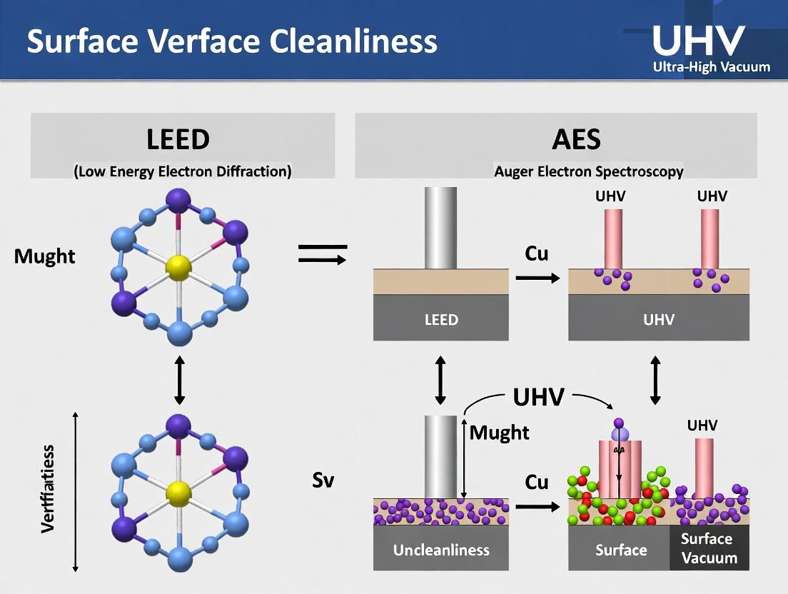
Foundations of Surface Science: Understanding LEED and AES Principles for UHV Cleanliness
The Critical Role of Surface Cleanliness in Biomedical Device Development and Advanced Materials
Surface cleanliness is a deterministic factor for the performance and biocompatibility of biomedical devices and advanced materials. Contaminant layers, even at sub-monolayer levels, can drastically alter surface energy, corrosion resistance, and protein adsorption profiles, leading to device failure or adverse biological responses. Within ultra-high vacuum (UHV) research and development, two primary surface-sensitive techniques are employed for cleanliness verification: Low-Energy Electron Diffraction (LEED) and Auger Electron Spectroscopy (AES). This guide compares their performance within the context of advanced biomedical material development.
Comparison Guide: LEED vs. AES for UHV Surface Analysis
Table 1: Core Technique Comparison
| Feature | Low-Energy Electron Diffraction (LEED) | Auger Electron Spectroscopy (AES) |
|---|---|---|
| Primary Information | Surface crystallographic structure & long-range order. | Elemental composition (except H, He) & chemical state. |
| Detection Limit | Indirect; disorder from ~1% of a monolayer. | Direct; typically 0.1 - 1.0 atomic %. |
| Spatial Resolution | Low (~1 mm). Typical for macro-area analysis. | High (< 10 nm possible with SAM). |
| Sample Damage Risk | Very low (typical beam currents ~1-100 nA). | Moderate (localized electron beam heating/desorption). |
| Key Strength for Cleanliness | Verifies atomic-level structural perfection. | Identifies and quantifies specific contaminant elements. |
| Key Limitation for Cleanliness | Cannot identify chemical nature of contaminants. | Poor sensitivity for light elements (C, O) on heavy substrates. |
Table 2: Experimental Data from a Titanium Alloy (Ti-6Al-4V) Study
| Analysis Parameter | LEED Results | AES Results | Interpretation |
|---|---|---|---|
| As-Received Surface | Diffuse background, no clear spots. | Strong C, O peaks; weak Ti, Al signals. | Amorphous carbonaceous/oily layer >5 nm thick. |
| After Ar+ Sputtering | Sharp (1x1) hexagonal pattern. | C peak reduced to ~15 at%, O ~45 at%, Ti increased. | Ordered Ti surface achieved, but persistent oxide & carbon. |
| After UHV Annealing at 800°C | Sharp, reconstructed patterns. | C < 5 at%, O ~30 at% (subsurface), Ti dominant. | Thermally cleaned surface; oxygen diffuses into bulk. |
Experimental Protocols
Protocol 1: Combined LEED/AES Analysis of Implant Surfaces
- Sample Mounting: Secure the biomedical sample (e.g., polished Ti alloy, stainless steel) on a UHV-compatible sample holder using tantalum clips.
- UHV Introduction: Transfer sample into the analysis chamber (base pressure ≤ 5×10⁻¹⁰ mbar).
- Initial Survey (AES): Acquire a survey spectrum (e.g., 20 eV to 2000 eV) from a representative ~500 µm area. Use primary beam: 10 keV, 10 nA.
- Initial Structural Check (LEED): Attempt LEED observation at electron energies 50-200 eV. Note pattern quality.
- In-situ Cleaning: Perform sequential Ar⁺ sputtering (1-3 keV, 15-30 minutes, sample current ~2 µA/cm²) with concurrent annealing up to 600°C (material dependent).
- Post-Cleaning Analysis: Iterate between AES (quantitative atomic% via sensitivity factors) and LEED until contaminant levels are minimized and a clear diffraction pattern is observed.
- Data Correlation: Correlate the reduction of AES carbon/oxygen signals with the emergence and sharpening of LEED patterns.
Protocol 2: Contamination Monitoring During Functionalization
- Establish Baseline: Clean sample as per Protocol 1 and record reference AES spectrum and LEED pattern.
- Ex-situ Functionalization: Remove sample from UHV; apply surface modification (e.g., silanization, peptide coating) under controlled (but non-UHV) environment.
- Re-introduction Analysis: Re-insert sample into UHV. Perform AES survey and high-resolution scans on key elements (C, N, O, substrate signals).
- Assessment: Calculate the increase in carbon signal and the attenuation of substrate signals to estimate coating thickness/coverage. LEED will typically show pattern extinction, confirming the presence of an amorphous adlayer.
Visualization of Method Selection
Title: Decision Workflow for LEED vs AES Surface Analysis
The Scientist's Toolkit: Key Research Reagents & Materials
Table 3: Essential Materials for UHV Surface Cleanliness Studies
| Item | Function & Rationale |
|---|---|
| UHV-Compatible Samples | Pre-polished coupons of materials (Ti, 316L SS, CoCr, Silicon). Must withstand high-temperature annealing. |
| High-Purity Argon Gas (99.9999%) | Source gas for ion sputter guns. High purity prevents implantation of new contaminants during cleaning. |
| UHV-Compatible Solvents | e.g., HPLC-grade isopropanol, acetone. For initial ex-situ degreasing to remove gross contamination. |
| Degassed Tantalum Foil/Clips | For sample mounting. Must be pre-outgassed to prevent being a contamination source in UHV. |
| Standard Reference Samples | e.g., Clean single crystal silicon (with native oxide) or gold. Used for instrument function verification. |
| Ion Sputter Gun (Ar+ Source) | Integrated into UHV system. Provides in-situ cleaning via physical sputtering of surface atoms. |
| Direct/Indirect Sample Heater | Capable of heating samples to ≥1000°C. Enables thermal desorption of contaminants and surface reconstruction. |
| Electron Gun & Hemispherical Analyzer | Core components of AES system for electron excitation and energy-resolved electron detection. |
| LEED Optics (Screen, Gun, Grids) | Integrated reverse-view optics for displaying elastically backscattered electron diffraction patterns. |
Thesis Context: Within the field of ultra-high vacuum (UHV) surface science, verifying surface cleanliness and atomic order is paramount. This guide compares Low-Energy Electron Diffraction (LEED) and Auger Electron Spectroscopy (AES) as complementary but distinct techniques for this purpose, focusing on LEED's unique ability to probe surface crystallography.
LEED vs. AES: Core Principles and Comparison
LEED and AES are foundational UHV techniques, but they provide fundamentally different information.
| Feature | Low-Energy Electron Diffraction (LEED) | Auger Electron Spectroscopy (AES) |
|---|---|---|
| Primary Information | Long-range surface crystallography, unit cell size & symmetry, surface order/disorder. | Surface chemical composition (elements except H, He), cleanliness verification. |
| Probing Mechanism | Elastic backscattering of low-energy electrons (20-200 eV). Wave interference creates diffraction patterns. | Inelastic scattering & core-hole decay. Measurement of characteristic Auger electron kinetic energies. |
| Data Output | Diffraction pattern (reciprocal space image). | Electron energy spectra (intensity vs. kinetic energy). |
| Key Metrics | Spot sharpness, background intensity, spot positions. | Peak positions (for element ID), peak heights/areas (for quantification). |
| Sensitivity | Extremely sensitive to atomic order and periodicity. Insensitive to amorphous contaminants. | Extremely sensitive to atomic composition (~0.1-1 at. %). Less sensitive to order. |
| Main Use in Cleanliness Verification | Verifies the structural quality of the substrate (e.g., a sharp (1x1) pattern). A dirty surface often shows high background or extra spots. | Directly identifies and quantifies chemical contaminants (e.g., C, O, S). |
Experimental Comparison: Verifying a Clean Si(100) Surface
Protocol 1: AES for Chemical Cleanliness Verification
- Sample Mounting: Install the Si sample on a UHV-compatible manipulator with heating capability.
- UHV Preparation: Pump system to base pressure (< 5 x 10⁻¹⁰ mbar).
- Electron Gun Alignment: Align a coaxial electron gun (typical beam: 3-10 keV, 10 nA-1 µA, ~100 nm spot) with the sample surface.
- Spectrum Acquisition: Sweep the analyzer's energy pass window (e.g., from 50 eV to 1000 eV kinetic energy) while collecting the first derivative (dN(E)/dE) of the electron energy distribution to enhance Auger peaks.
- Data Analysis: Identify peaks via known kinetic energies: Si LVV (~92 eV), O KLL (~503 eV), C KLL (~272 eV).
- Cleanliness Criterion: A surface is considered chemically clean when the peak-to-peak heights of major contaminant signals (C, O) are ≤ 1% of the dominant substrate peak (Si).
Protocol 2: LEED for Crystallographic Order Verification
- Post-AES Verification: Use the same sample prepared for AES.
- LEED Setup: Position the sample in front of a display-type LEED optics (typically 4-grid). The system consists of a fluorescent screen, biased grids, and an electron gun.
- Electron Beam Conditions: Direct a collimated, monochromatic electron beam (typically 50-150 eV, current ~1-100 nA) at normal incidence onto the sample.
- Diffraction Pattern Observation: Apply retardation voltages to the grids to allow only elastically scattered electrons to reach the screen. The resulting pattern is a direct image of the surface's reciprocal lattice.
- Pattern Analysis: For a clean, well-ordered Si(100) surface, expect a sharp (2x1) reconstruction pattern due to dimerization. Assess spot sharpness, background intensity, and presence of reconstruction spots versus a simple (1x1) pattern.
- Order Criterion: A high-quality surface shows bright, sharp diffraction spots on a low-background screen.
Quantitative Comparison of LEED and AES Data
The table below presents typical experimental data from a study preparing a clean nickel (Ni(100)) surface through cycles of sputtering and annealing.
| Condition | AES Peak-to-Peak Ratio (C/Ni, O/Ni) | LEED Pattern Observation | Conclusion |
|---|---|---|---|
| As-Inserted | C: 0.45, O: 0.60 | No discernible spots; high diffuse background. | Heavily contaminated, disordered surface. |
| After Sputter (1 cycle) | C: 0.15, O: 0.10 | Faint, diffuse (1x1) spots; very high background. | Residual contaminants; poor crystallinity. |
| After Anneal (700°C) | C: 0.03, O: 0.02 | Bright, sharp (1x1) spots; low background. | Chemically clean and well-ordered surface. |
| After Brief Air Exposure | C: 0.25, O: 0.40 | High background, very faint spots. | Rapid contamination degrades both chemistry and order. |
The Scientist's Toolkit: Essential Research Reagent Solutions for UHV Surface Science
| Item | Function / Explanation |
|---|---|
| UHV System (≤10⁻¹⁰ mbar) | Provides contamination-free environment where surface lifetimes are hours to days, enabling accurate analysis. |
| Ion Sputtering Gun (Ar⁺) | Supplies inert gas ions (typically Ar⁺ at 0.5-5 keV) for physical removal of surface contaminants via momentum transfer. |
| Sample Heater (e-beam or radiative) | Allows thermal annealing to heal sputter damage, induce reconstruction, and promote surface diffusion for ordering. |
| LEED Optics (4-Grid) | Integrated electron gun and display system for visualizing the surface reciprocal lattice via elastic backscattering. |
| Cylindrical Mirror Analyzer (CMA) or Concentric Hemispherical Analyzer (CHA) | High-sensitivity electron energy filter for collecting Auger electron spectra to determine chemical composition. |
| Standard Reference Samples (e.g., Au foil) | Provides known, clean surfaces (Au(111)) for instrument calibration and energy scale verification. |
Visualization: UHV Surface Analysis Workflow
Title: Workflow for UHV Surface Cleanliness and Order Verification
Visualization: Information Yield from LEED vs. AES
Title: Physical Principles and Data Output of LEED and AES
In the context of Ultra-High Vacuum (UHV) surface cleanliness verification, researchers must choose between powerful analytical techniques. This guide compares Auger Electron Spectroscopy (AES) with Low-Energy Electron Diffraction (LEED) for surface analysis, focusing on their efficacy in identifying elemental composition and contaminants—a critical concern in fields like semiconductor fabrication and pharmaceutical device development.
Core Physics of AES
Auger Electron Spectroscopy (AES) functions by focusing a primary electron beam (typically 3-10 keV) onto a solid surface in UHV. This beam ionizes a core-level electron from a target atom. An electron from a higher energy level fills this vacancy, and the released energy ejects a third electron—the Auger electron. The kinetic energy of this ejected Auger electron is characteristic of the parent element, enabling qualitative and quantitative analysis of the top 2-10 nanometers of the surface.
Performance Comparison: AES vs. LEED for Cleanliness Verification
While both AES and LEED are UHV surface science techniques, their primary functions differ significantly. LEED excels at determining surface crystalline structure and ordering, whereas AES is optimized for direct elemental identification and contaminant detection.
Table 1: Core Analytical Capabilities Comparison
| Feature | Auger Electron Spectroscopy (AES) | Low-Energy Electron Diffraction (LEED) |
|---|---|---|
| Primary Output | Elemental composition (all except H, He), chemical state hints. | Surface crystallographic structure, symmetry, unit cell size. |
| Detection Capability | Direct detection of contaminant atoms (C, O, S, etc.). | Indirect; infers cleanliness from quality of diffraction pattern. |
| Information Depth | 2-10 nm (escape depth of Auger electrons). | 0.5-1 nm (very surface sensitive due to low e- energy). |
| Lateral Resolution | Excellent (~10 nm in SAM mode). | Poor (beam diameter ~0.5-1 mm). |
| Quantification | Semi-quantitative (accuracy ~20-30% atomic). | Not applicable for composition. |
| Best For | Identifying what contaminants are present. | Assessing if the surface is atomically ordered/clean. |
Table 2: Supporting Experimental Data from UHV Surface Studies
| Experiment Objective | AES Results | LEED Results | Conclusion |
|---|---|---|---|
| Verify Si(100) wafer cleaning | Detected 0.8 at.% carbon, 0.2 at.% oxygen post-anneal. | Showed sharp (2x1) reconstruction pattern. | AES confirms trace contaminants; LEED confirms ordered surface. |
| Assess metal surface oxidation | Identified increasing O KLL peak; metal peak attenuation. | Pattern degraded and disappeared as oxide amorphous layer grew. | AES quantified oxide growth; LEED signaled loss of crystalline order. |
| Map particulate contamination | SAM image showed 50nm carbon-rich particle on Ni surface. | No spatial information on contaminant; overall pattern was weak. | AES directly imaged and identified the contaminant source. |
Experimental Protocols for UHV Surface Verification
Protocol 1: Combined AES/LEED Analysis of Surface Cleanliness
- Sample Introduction: Load sample into UHV chamber (< 10⁻⁹ mbar).
- Initial LEED: Acquire a LEED pattern at electron energies 50-150 eV to establish baseline surface order.
- AES Survey Scan: Using a 10 keV, 10 nA primary beam, acquire a survey spectrum from 20 eV to 2000 eV.
- Data Analysis: Identify all elements present from characteristic Auger peaks (e.g., C KLL at ~272 eV, O KLL at ~503 eV).
- Sputter Cleaning: Use inert gas ion sputtering (Ar⁺, 1 keV) to remove surface layers.
- Iterative Measurement: Repeat steps 2 and 3 until AES shows contaminant peaks are minimized and LEED shows a sharp, well-defined pattern.
- Quantification: Use relative sensitivity factors to calculate approximate atomic concentrations from AES peak-to-peak heights in derivative spectrum.
Protocol 2: Contaminant Depth Profiling via AES
- Surface Measurement: Acquire high-resolution AES spectrum of key element peaks (e.g., C, O, substrate).
- Ion Sputtering: Begin controlled etching with a focused Ar⁺ ion gun (typical 1-5 keV).
- Cyclic Analysis: Interrupt sputtering at fixed time intervals to acquire AES spectra at the same spot.
- Data Compilation: Plot atomic concentration (from AES) vs. sputter time (converted to depth using a calibration standard).
- Interpretation: Determine if contaminants are surface-adventitious or have diffused into the bulk.
Visualization of AES Process and Workflow
Title: Three-Step Auger Electron Emission Process
Title: Combined AES & LEED Surface Cleanliness Workflow
The Scientist's Toolkit: Key Research Reagent Solutions for AES
Table 3: Essential Materials for AES Surface Analysis
| Item | Function in AES Analysis |
|---|---|
| Standard Reference Samples (e.g., pure Cu, Ag) | Used for instrument calibration (energy scale, resolution) and quantification sensitivity factors. |
| Argon Gas (Ultra-High Purity) | Source gas for the ion sputter gun used for in-situ sample cleaning and depth profiling. |
| Conductive Mounting Tabs (e.g., Carbon Tape) | Provides electrical and thermal contact between sample and holder to prevent charging. |
| UHV-Compatible Sample Holders | Typically made of Mo or Ta, designed for direct resistive heating for in-situ sample annealing. |
| Electron Gun Filament (W or LaB₆) | Source of the primary electron beam. A consumable item requiring periodic replacement. |
| Calibrated Ion Sputter Source | Provides a known flux of inert ions for controlled, quantifiable material removal. |
In pharmaceutical research, the precise engineering of solid dosage forms or catalytic drug synthesis pathways often begins at the atomic level on Ultra-High Vacuum (UHV) surfaces. Defining "cleanliness" for these surfaces is not subjective; it is a quantitative requirement dictated by the need for reproducible adsorption and reaction studies of Active Pharmaceutical Ingredients (APIs) and excipients. The central thesis in modern verification research pits Low-Energy Electron Diffraction (LEED), sensitive to surface order, against Auger Electron Spectroscopy (AES), sensitive to surface elemental composition. This guide compares their performance in establishing contamination thresholds critical for pharma-relevant surface science.
Comparative Analysis: LEED vs. AES for Cleanliness Verification
Table 1: Core Performance Comparison
| Parameter | Low-Energy Electron Diffraction (LEED) | Auger Electron Spectroscopy (AES) |
|---|---|---|
| Primary Sensitivity | Long-range periodic order of surface atoms. | Elemental identity of top 3-10 atomic layers (Z≥3). |
| Detection Limit (Typical) | ~1% of a monolayer (for ordered contaminants). | 0.1% - 1.0% of a monolayer. |
| Spatial Resolution | ~1 mm (standard); low for mapping. | ~10 nm (modern systems); excellent for mapping. |
| Quantification | Indirect; based on spot sharpness/background. | Direct; via peak-to-peak height sensitivity factors. |
| Key Strength for Pharma | Verifies substrate order for templated organic film growth. | Directly detects & quantifies C, O, S, N contaminants from APIs/air. |
| Critical Limitation | Insensitive to amorphous carbon or disordered adsorbates. | Can damage sensitive organic adsorbates with electron beam. |
| Typical UHV Base Pressure Requirement | < 5 x 10⁻¹¹ mbar | < 1 x 10⁻¹⁰ mbar |
Table 2: Experimental Data from a Model Study (Pt(111) Surface)
| Surface Condition | LEED Observation | AES Atomic % | Conclusion for Pharma Research |
|---|---|---|---|
| Ideal Clean | Sharp (1x1) hexagonal pattern. | C: 0.5%, O: 0.2%, Pt: 99.3% | Baseline for catalytic studies of chiral synthesis. |
| After Ambient Exposure | Slightly increased background. | C: 12.4%, O: 8.7%, Pt: 78.9% | Hydrocarbon/Oxygen threshold for unreliable API adsorption. |
| After Sputter Clean | Sharp (1x1) pattern restored. | C: <0.8%, O: <0.5%, Pt: >98.7% | Validated cleaning protocol. |
| After Glycine Adsorption | New, ordered superstructure pattern. | C: 15.2%, N: 4.8%, O: 9.1% | LEED confirms ordered layer; AES quantifies stoichiometry. |
Experimental Protocols for Threshold Determination
Protocol 1: Establishing a Carbon Threshold via AES
- Preparation: A single-crystal metal substrate (e.g., Au(111)) is prepared in UHV via repeated Ar⁺ sputtering (1 keV, 15 µA, 30 min) and annealing (720°C, 2 min) cycles.
- Baseline Measurement: AES survey scan (3 keV primary beam, 1 µA, 0.5 eV step) is taken from 20-1000 eV. Peak-to-peak heights (PPH) for C(KLL) at 272 eV and Au(MNN) at 2024 eV are recorded.
- Controlled Contamination: The surface is exposed to calibrated doses of ethylene (C₂H₄) via a leak valve, simulating hydrocarbon backstreaming.
- Quantification: After each dose, AES scans are repeated. The relative atomic concentration of Carbon is calculated using standard sensitivity factors:
C at.% = [I_C/S_C] / [I_C/S_C + I_Au/S_Au]. The process continues until the C level surpasses the predetermined threshold (e.g., 2 at.%). - Correlation: The equivalent Langmuir exposure causing this threshold is recorded as a critical parameter for chamber operation.
Protocol 2: Correlating Order (LEED) with Composition (AES)
- Initial Verification: A clean Si(100)-2x1 surface is confirmed via a sharp 2x1 LEED pattern (80 eV) and AES showing minimal O and C.
- Organic Deposition: A sub-monolayer of a model pharmaceutical compound (e.g., ibuprofen) is thermally evaporated onto the room-temperature substrate.
- Sequential Analysis:
- Step A: LEED pattern is immediately observed (40-120 eV). A transition from sharp spots to a diffuse background indicates a disordered, amorphous layer.
- Step B: AES scan (5 keV, 0.1 µA to minimize damage) is performed on a nearby spot to quantify the C and O coverage.
- Annealing Study: The surface is progressively annealed in steps (50°C, 1 min). After each step, LEED and AES are repeated. The appearance of a new, ordered LEED pattern concurrent with a specific AES stoichiometry defines the "clean" threshold for a well-ordered organic interface.
Visualizations
Workflow for Establishing UHV Cleanliness Thresholds
LEED vs AES Decision Logic for Pharma Surfaces
The Scientist's Toolkit: Essential Research Reagents & Materials
Table 3: Key Research Reagent Solutions for UHV Surface Preparation
| Item | Function in Pharma-Relevant UHV Research |
|---|---|
| Single-Crystal Substrates (e.g., Au(111), Pt(111), Si(100)) | Provide atomically flat, well-defined model surfaces for fundamental adsorption studies of API molecules. |
| High-Purity Sputter Gases (Ar, Kr, 99.9999%) | Inert gases ionized to physically remove contaminated surface layers via momentum transfer. |
| Calibrated Leak Valves & Exposure Sources | Enable precise, reproducible dosing of model pharmaceutical vapors (e.g., solvents, simple APIs) or contaminant gases (CO, C₂H₄). |
| Electron-Beam Evaporators | Used to deposit ultra-thin, clean films of metal contacts or barriers relevant to organic electronic drug delivery devices. |
| Organic Molecular Beam Epitaxy (OMBE) Sources | Thermally evaporate intact, high-purity pharmaceutical molecules onto the UHV surface for monolayer studies. |
| Standard Reference Materials (e.g., Au foil for AES, Graphite for C calibration) | Essential for quantitative calibration and accuracy verification of surface analysis instruments. |
In the comparative research of Low-Energy Electron Diffraction (LEED) and Auger Electron Spectroscopy (AES) for surface cleanliness verification, the fundamental requirement of an Ultra-High Vacuum (UHV) environment is paramount. This guide compares the impact of vacuum level on data integrity for both techniques, underscoring why UHV is non-negotiable.
The Critical Role of Vacuum: LEED vs. AES Performance
The core function of a UHV environment (typically ≤ 10⁻⁹ mbar) is to minimize surface contamination from residual gases, ensuring the analysis reflects the true sample surface. The mean free path of electrons is drastically reduced at higher pressures, and adsorption events can occur in seconds, corrupting data.
Quantitative Comparison: Vacuum Level vs. Signal Integrity
The following table summarizes experimental data on the degradation of key metrics for LEED and AES at sub-optimal vacuum levels.
Table 1: Impact of Vacuum Pressure on LEED and AES Analysis
| Vacuum Pressure (mbar) | Approx. Time to Form a Monolayer | LEED Spot Sharpness (Arb. Units) | AES Peak (C KLL) Intensity (Arb. Units) | Dominant Contaminant |
|---|---|---|---|---|
| Ultra-High Vacuum (1x10⁻¹⁰) | ~10 hours | 100 (Reference) | 100 (Reference) | Negligible |
| High Vacuum (1x10⁻⁷) | ~1 minute | 45 | 30 | Hydrocarbons (C, O) |
| Medium Vacuum (1x10⁻⁴) | < 0.1 seconds | Not Obtainable | 5 (Buried in noise) | H₂O, CO, CO₂ |
Experimental Protocols for UHV-Dependent Verification
Protocol 1: Base Pressure Attainment & Bake-Out
Objective: Achieve a stable UHV environment (< 5x10⁻¹⁰ mbar) prior to sample introduction.
- Rough Pumping: Use a rotary vane pump to reach ~10⁻³ mbar.
- High Vacuum Pumping: Engage a turbomolecular or cryogenic pump to reach ~10⁻⁸ mbar.
- System Bake-Out: Heat the entire chamber to 120-200°C for 12-48 hours using heating tapes. This desorbs water and other volatiles from chamber walls.
- UHV Activation: Activate ion pumps and/or titanium sublimation pumps. Cool cryoshrouds with liquid nitrogen if applicable.
- Validation: Monitor pressure with a Bayard-Alpert ionization gauge. The system is ready when pressure stabilizes below the target for 2+ hours post-bake.
Protocol 2: In-Situ Sample Preparation & AES/LEED Sequential Analysis
Objective: Prepare a clean surface and verify it with combined AES and LEED without breaking vacuum.
- Sample Transfer: Introduce the sample (e.g., single crystal metal) via a UHV-compatible load-lock or transfer arm.
- In-Situ Cleaning:
- Sputtering: Bombard the surface with Ar⁺ ions (1-5 keV, 10-20 µA/cm²) for 15-30 minutes.
- Annealing: Resistively heat the sample to a specified temperature (often 600-900°C for metals) for 1-5 minutes to heal crystal damage.
- AES Verification:
- Set primary electron beam: 3-5 keV, 10 nA-1 µA.
- Acquire survey spectrum (e.g., 0-1000 eV).
- Success Criterion: Peak-to-peak heights of contaminant peaks (C, O) are < 1% of the strongest substrate peak.
- LEED Verification:
- Reduce electron beam energy to 50-200 eV.
- Project the diffraction pattern onto a phosphor screen.
- Success Criterion: Appearance of sharp, bright diffraction spots with low background intensity.
The Scientist's Toolkit: Research Reagent Solutions for UHV Surface Science
Table 2: Essential Materials for UHV Surface Cleanliness Experiments
| Item | Function in UHV Research |
|---|---|
| UHV-Compatible Single Crystal Sample (e.g., Ni(100), Cu(111)) | Provides a well-defined, reproducible surface with known crystallographic orientation for fundamental studies. |
| Research-Grade Sputtering Gas (99.9999% Ar) | High-purity argon minimizes implantation of new contaminants during ion bombardment cleaning cycles. |
| UHV-Compatible Sample Mounting Materials (e.g., High-Purity Ta or W wires, Al₂O₄ Adhesives) | Withstand high-temperature annealing without outgassing contaminants that redeposit on the sample. |
| Electron-Emissive Phosphor Screen (UHV Degassed) | Coated on the LEED viewport, it converts the pattern of diffracted electrons into visible light without contaminating the chamber. |
| In-Situ Evaporation Sources (e.g., Knudsen Cells, e-beam evaporators) | Allow for the deposition of ultrathin, clean films of metals or organics onto the verified substrate for subsequent analysis. |
Visualization of Experimental Workflow and Logical Relationships
Title: UHV Sample Preparation and Verification Workflow
Title: Signal Degradation in Poor Vacuum for AES and LEED
From Theory to Bench: Step-by-Step Methodologies for LEED and AES in Cleanliness Verification
Within the broader research thesis comparing Low-Energy Electron Diffraction (LEED) and Auger Electron Spectroscopy (AES) for Ultra-High Vacuum (UHV) surface cleanliness verification, establishing a robust and reproducible LEED protocol is critical. LEED provides direct, visual information on surface periodicity and cleanliness through distinct diffraction patterns. This guide compares key instrumental components and methodological choices in the LEED workflow, from sample introduction to pattern acquisition, providing data to inform optimal setup for surface science and materials research.
Comparison of LEED Instrumentation Components
The performance of a LEED verification protocol is highly dependent on the choice of hardware. The following table compares common alternatives for core components.
Table 1: Comparison of Key LEED System Components
| Component & Alternatives | Key Performance Metrics | Typical Experimental Data / Outcome | Primary Advantage | Primary Disadvantage |
|---|---|---|---|---|
| Sample Mounting: Direct vs. Transferrable Holder | Thermal & electrical contact, heating/cooling rate, positional reproducibility. | Sample outgassing rate: Direct mount ~1e-10 Torr/min vs. Transferrable ~1e-9 Torr/min post-insertion. | Direct: Superior thermal management, minimal contamination risk. | Lack of sample library flexibility. |
| Manipulator: XYZθ vs. XYZθφχ | Angular freedom, precision of azimuthal alignment (±°). | Time to align for pattern: XYZθ: 5-10 min; XYZθφχ: <2 min. | XYZθφχ: Enables perfect zone-axis alignment for any crystal face. | Higher cost, more complex. |
| Electron Gun: Tungsten vs. LaB₆ Cathode | Beam current stability, brightness, operational lifetime (hrs). | Beam current @ 100 eV: W: 0.5 µA ±5%; LaB₆: 2.0 µA ±1%. Pattern clarity significantly improved with LaB₆. | LaB₆: Higher brightness for sharper patterns at lower beam energies. | Requires higher vacuum (<1e-10 Torr) for longevity. |
| Detector: Microchannel Plate (MCP) + Fluorescent Screen vs. Retarding Field Analyzer (RFA) | Sensitivity, signal-to-noise, background suppression. | Pattern acquisition time for weak signal: MCP: 30 sec; RFA (scanning): 5-10 min. | MCP: Direct, real-time visual imaging; superior for low currents. | Potential saturation from high-intensity beams. |
| Camera: CCD vs. sCMOS | Quantum efficiency (%), read noise (e-), dynamic range. | Pattern resolution: CCD captures 8-bit (256 levels); sCMOS captures 16-bit (65,536 levels), revealing faint superstructure spots. | sCMOS: Higher dynamic range critical for quantitative I-V LEED analysis. | Higher data storage requirements. |
Detailed Experimental Protocols
Protocol A: Sample Mounting and Preparation for LEED
- Ex-Situ Cleaning: Cut sample to <10x10mm. Sequentially sonicate in acetone, isopropanol, and deionized water for 5 minutes each.
- Mounting: For direct mounting, spot-weld 0.5mm Ta or W wires between sample edge and holder posts. For transferrable holders, secure with Ta clips.
- UHV Insertion: Load into UHV via load-lock. Pump in load-lock to <1e-8 Torr before transfer to preparation chamber.
- In-Situ Preparation: In the preparation chamber, heat sample via electron bombardment or resistive heating to 600-800°C (for metals) or 500°C (for oxides) for 15-30 minutes. Optionally, use cycles of Ar⁺ sputtering (500 eV, 1-2 µA/cm², 15 min) followed by annealing.
- Transfer: Move the sample to the analysis chamber, ensuring the manipulator is correctly engaged. Base pressure must be <5e-11 Torr for optimal LEED.
Protocol B: LEED Pattern Acquisition and Verification
- System Check: Ensure the fluorescent screen or MCP detector is at high voltage (~5 kV). Set camera to appropriate gain.
- Beam Alignment: Energize electron gun to a standard 80-120 eV. Adjust gun alignment lenses to center the beam spot on the sample.
- Pattern Optimization: Set electron beam energy between 40 eV and 200 eV. Adjust beam current (0.1-5 µA) and sample position (Z) to achieve a bright, focused pattern on the screen.
- Cleanliness Verification: Acquire pattern. A clean, well-ordered surface will produce sharp, bright diffraction spots with low background intensity. A contaminated or disordered surface shows spot broadening, high background, or extraneous rings.
- Documentation: Capture image via camera. Record exact beam energy (eV), current (µA), sample temperature (K), and any sample bias (V).
Visualization of the LEED Verification Workflow
Diagram Title: LEED Surface Verification Protocol Workflow
The Scientist's Toolkit: Key Research Reagent Solutions
Table 2: Essential Materials for the LEED Verification Protocol
| Item | Function & Rationale |
|---|---|
| UHV-Compatible Sample Plates (Mo, Ta, W) | Provide a clean, refractory, and electrically conductive mounting surface. Molybdenum is common for its machinability and high melting point. |
| Tantalum or Tungsten Wire (0.25mm & 0.5mm) | Used for spot-welding samples to holders or securing with clips. High purity minimizes contamination during high-temperature annealing. |
| High-Purity Argon Gas (99.9999%) | Inert sputtering gas for in-situ ion bombardment cleaning. High purity prevents implantation of reactive gases (e.g., O₂, N₂) into the sample. |
| Calibrated Leak Valve | Allows precise, controlled introduction of research gases (O₂, H₂, CO) for surface reaction studies post-cleanliness verification. |
| NIST-Traceable Thermocouple (Type C or K) | For accurate sample temperature measurement during annealing cycles. Critical for reproducible surface reconstruction. |
| Standard Reference Sample (e.g., Pt(111) or Si(100) wafer) | A well-characterized surface used to verify the operational integrity and calibration of the LEED system (spot positions, energy dependence). |
In Ultra-High Vacuum (UHV) surface science, verifying cleanliness is paramount. Low-Energy Electron Diffraction (LEED) provides structural information but is insensitive to light elements and chemical state. Auger Electron Spectroscopy (AES), with its high spatial resolution and sensitivity to elements (Z≥3), is a cornerstone for direct chemical contamination assessment. This guide compares the AES verification protocol against alternative techniques, focusing on its specific workflow of survey scans, multiplexing, and depth profiling.
Comparative Performance: AES vs. Alternative Techniques
The following table compares key surface analysis techniques for UHV cleanliness verification.
Table 1: Technique Comparison for UHV Surface Cleanliness Verification
| Feature | AES | X-ray Photoelectron Spectroscopy (XPS) | Low-Energy Electron Diffraction (LEED) | Secondary Ion Mass Spectrometry (SIMS) |
|---|---|---|---|---|
| Primary Information | Elemental (Z≥3) | Elemental & Chemical State | Surface Structure | Elemental & Molecular (Trace) |
| Spatial Resolution | ~10 nm (Excellent) | 3-10 µm (Good) | ~0.5 mm (Poor) | 50 nm - 1 µm (Very Good) |
| Detection Limit | 0.1-1 at% (Good) | 0.1-1 at% (Good) | N/A (Structural) | ppb-ppm (Excellent) |
| Depth Resolution | 2-5 nm (Info Depth) | 2-10 nm (Info Depth) | 1-2 atomic layers | < 1 nm (Excellent) |
| Sample Damage | Moderate (e-beam) | Very Low | Very Low | High (Sputtering) |
| Speed of Analysis | Very Fast | Slow | Fast | Slow/Moderate |
| Quantitative Ease | Good (with standards) | Excellent (semi-standardless) | Qualitative | Poor (needs standards) |
| Key Strength for Cleanliness | Fast mapping, high-resolution depth profiling | Chemical state identification, standardized quantification | Long-range order check | Ultimate trace sensitivity, hydrogen detection |
The AES Verification Protocol: Detailed Experimental Methodologies
Survey Scans: Initial Contamination Assessment
Protocol: A wide energy scan (e.g., 20 eV to 2000 eV) is performed at a primary beam energy (Ep) of 10 keV, beam current of 10 nA, and modulation amplitude of 5 eV. The scan is performed at multiple random locations on the sample to assess homogeneity. Purpose: To identify all elements present above ~0.5 at% concentration. Key contaminants like C, O, S, Cl, and Ca are immediately visible. Data Comparison: Compared to XPS survey scans, AES surveys are typically faster and offer better spatial localization but lack direct chemical bonding information.
Multiplexing: High-Resolution Elemental Quantification
Protocol: After identifying elements from the survey, high-resolution narrow scans (e.g., 20 eV windows) are acquired over the principal Auger transitions for each element (e.g., C KLL at 272 eV, O KLL at 503 eV). Multiple scans are averaged to improve signal-to-noise. Purpose: Accurate measurement of peak-to-peak height (in derivative mode) or peak area (in direct mode) for quantification using relative sensitivity factors (RSFs). Quantitative Data Example: Table 2: Multiplex Scan Data for a Cleaned Metal Substrate
| Element | Peak Energy (eV) | Measured Peak-to-Peak Height (arb. units) | Relative Sensitivity Factor (RSF) | Calculated Atomic % |
|---|---|---|---|---|
| Substrate (M) | 650 | 120,000 | 0.25 | 94.7% |
| Carbon | 272 | 5,500 | 0.20 | 3.1% |
| Oxygen | 503 | 3,800 | 0.40 | 1.1% |
| Sulfur | 152 | 900 | 0.65 | 1.1% |
Depth Profiling: In-Depth Contamination Analysis
Protocol: Sequential or simultaneous combination of ion sputtering (e.g., 1-5 keV Ar⁺ ions) with AES analysis. A sputter crater is created, and multiplex scans are taken at intervals. Sputter time is converted to depth using a calibrated sputter rate for a reference material (e.g., Ta₂O₅). Purpose: Determine the distribution of contaminants as a function of depth—distinguishing surface adsorbates from bulk segregation or interface impurities. Performance Data: AES depth profiling offers superior depth resolution (1-3 nm) in the topmost layers compared to XPS, but SIMS provides better resolution and sensitivity at trace levels.
Table 3: Depth Profiling Performance Comparison
| Parameter | AES Depth Profiling | XPS Depth Profiling | Dynamic SIMS |
|---|---|---|---|
| Best Depth Resolution | 1-3 nm | 2-5 nm | < 1 nm |
| Detection Limit in Profile | ~0.1 at% | ~0.5-1 at% | ppb-ppm range |
| Chemical State Info | Limited (peak shape) | Preserved | Lost |
| Artifact Potential | Electron beam induced damage, preferential sputtering | Reduced charging, preferential sputtering | High: ion implantation, matrix effects |
Visualizing the AES Verification Workflow
AES Cleanliness Verification Protocol Decision Workflow
The Scientist's Toolkit: Key Research Reagent Solutions
Table 4: Essential Materials for AES Surface Cleanliness Studies
| Item | Function in Experiment |
|---|---|
| UHV-Compatible Sample Holders | Provides electrical and thermal contact, minimizes outgassing. Often made of Ta or Mo. |
| Reference Standard (e.g., Pure Au, Cu foil) | Used for energy calibration and verifying analyzer performance before critical measurements. |
| Argon Gas (99.9999% purity) | Source gas for the ion sputter gun used in sample cleaning and depth profiling. |
| Ion Sputter Gun (differential pumping) | Generates focused Ar⁺ beam for in-situ cleaning and depth profiling within the UHV chamber. |
| Electron Gun (Field Emission or LaB₆) | Provides the primary, focused electron beam to excite Auger electron emission from the sample. |
| Cylindrical Mirror Analyzer (CMA) or CHA | The energy analyzer that measures the kinetic energy distribution of emitted Auger electrons. |
| Relative Sensitivity Factor (RSF) Library | Database of elemental sensitivity factors for the specific instrument, enabling quantitative analysis. |
| Conductive Adhesive (e.g., Carbon Tape) | For mounting non-conductive or poorly conducting samples to prevent charging artifacts. |
| In-situ Cleaver/Scraper/Heater | Tools for preparing fresh, clean surfaces inside UHV to establish a true cleanliness baseline. |
Comparison Guide: LEED vs. AES for UHV Surface Cleanliness Verification
This guide compares the performance of Low-Energy Electron Diffraction (LEED) and Auger Electron Spectroscopy (AES) as primary techniques for verifying surface cleanliness and order in Ultra-High Vacuum (UHV) research.
Quantitative Performance Comparison
Table 1: Core Performance Metrics for Surface Analysis
| Metric | LEED | AES | Notes / Experimental Conditions |
|---|---|---|---|
| Primary Information | Surface periodicity, reconstruction, disorder. | Elemental surface composition (Z≥3). | LEED probes long-range order; AES probes chemical identity. |
| Spatial Resolution | ~0.1-1 mm (standard). <0.1 µm (µLEED). | ~10 nm - 1 µm (modern systems). | Data from recent instrument specifications (2023-2024). |
| Detection Limit (ML) | ~0.05 ML for ordered structures. | ~0.01-0.1 at% (varies by element). | AES is superior for trace contaminant detection. |
| Probe Depth | 5-20 Å (very surface sensitive). | 20-100 Å (escape depth of Auger electrons). | LEED is more sensitive to the topmost atomic layer. |
| Vacuum Requirement | UHV (<10⁻⁹ mbar) | UHV (<10⁻⁹ mbar) | Mandatory for both to preserve surface integrity. |
| Sample Damage Risk | Low (beam currents ~1-100 nA). | Medium-High (localized heating, electron-stimulated desorption). | Protocols require minimized beam exposure for sensitive samples. |
| Quantitative Analysis | Spot intensity vs voltage (I-V) for structure. | Directly quantitative with standards/sensitivity factors. | AES provides straightforward atomic concentration percentages. |
| Time per Analysis | Seconds for pattern; minutes for I-V curves. | Seconds to minutes per point/scan. |
Table 2: Application-Specific Suitability for Cleanliness Verification
| Surface Condition / Goal | Recommended Technique | Supporting Experimental Data |
|---|---|---|
| Initial Gross Contamination Check | AES | Survey scans (20-2000 eV) identify C, O, S, and common contaminants in <60 sec. |
| Verifying Atomic-Level Order | LEED | Sharp, bright diffraction spots with low background confirm a clean, well-ordered surface. |
| Detecting Amorphous Overlayers | AES + LEED | AES detects contaminant elements; LEED shows diffuse patterns or spot attenuation. |
| Quantifying Reconstructed Surfaces | LEED I-V + AES | I-V curves determine reconstruction model; AES confirms absence of contaminant-driven reconstruction. |
| Mapping Contaminant Distribution | Scanning AES (SAES) | SAES maps (e.g., C-KLL, O-KLL) show spatial distribution of adsorbates at µm-scale. |
| Monitoring In-Situ Cleaning (e.g., sputtering) | AES | Sequential spectra provide real-time, quantitative tracking of contaminant removal rates. |
Experimental Protocols
Protocol 1: Combined LEED/AES Cleanliness Verification Workflow
- Sample Transfer: Introduce sample into UHV system via load-lock. Bake system to achieve base pressure < 5 x 10⁻¹⁰ mbar.
- Initial AES Survey: Using a primary electron beam (Ep=3-10 keV, I~10 nA, beam diameter ~500 nm), acquire a survey spectrum from 20 to 2000 eV. Identify all elements present.
- Quantitative AES: Acquire high-resolution multiplex scans for key contaminant (C, O) and substrate peaks. Use relative sensitivity factors to calculate atomic concentrations.
- Criteria Check: If contaminant levels exceed threshold (typically >5-10 at% total), proceed to in-situ cleaning (e.g., Ar⁺ sputtering, annealing).
- Post-Cleaning LEED: Using electron beam (Ep=50-200 eV, I~1 nA), acquire LEED pattern. Key indicators of cleanliness are:
- Sharp Spots: Low spot full-width at half-maximum (FWHM).
- Low Background: Diffuse scattering between spots is minimal.
- Expected Symmetry: Pattern matches the known symmetry of the substrate surface.
- Final AES Verification: Perform a final AES survey to confirm no recontamination occurred during annealing/analysis.
Protocol 2: LEED I-V for Distinguishing Reconstruction from Disorder
- Pattern Acquisition: Center the (0,0) or a fundamental Bragg beam on the screen.
- Data Collection: Increment the beam energy (e.g., from 30 to 400 eV in 1-2 eV steps). At each energy, digitally record the integrated intensity of the chosen diffraction spot.
- Background Subtraction: Measure background intensity near the spot and subtract.
- Analysis: Compare the resulting I-V curve to multiple scattering dynamical calculations for different structural models. A good match confirms a specific reconstruction. A weak, poorly defined I-V curve suggests a disordered surface.
Mandatory Visualizations
Integrated UHV Surface Verification Workflow
LEED Pattern Decision Logic for Cleanliness & Order
The Scientist's Toolkit: Key Research Reagents & Materials
Table 3: Essential Materials for UHV Surface Preparation & Analysis
| Item | Function in Experiment |
|---|---|
| Single Crystal Substrate (e.g., Pt(111), Si(100)) | Provides a well-defined, atomically flat starting surface for study. |
| UHV-Compatible Sample Holder (e.g., Mo or Ta foil clips) | Securely holds the sample, allows resistive heating, and provides reliable electrical contact. |
| High-Purity Sputter Gas (Ar, 99.9999%) | Used for ion sputtering to remove surface contaminants and oxides via physical bombardment. |
| UHV-Compatible Electron Bombardment Heater | Enables high-temperature annealing (>1000°C) to re-order the surface after sputtering or induce reconstruction. |
| High-Purity Calibration Materials (e.g., Au, Cu foils) | Used for energy scale calibration of the AES spectrometer and work function checks. |
| In-Situ Cleaver (for cleavable crystals like GaAs(110)) | Provides a method to create a fresh, uncontaminated surface within the UHV environment. |
| LEED/AES Intensity Standard (e.g., a well-characterized W(110) crystal) | Allows for inter-laboratory comparison and verification of instrument response functions. |
| UHV-Compatible Leak Valve & Dosage Tube | For controlled introduction of research gases (O₂, H₂, CO) for surface reaction studies post-cleanliness verification. |
Introduction Within the ongoing research debate on Low Energy Electron Diffraction (LEED) versus Auger Electron Spectroscopy (AES) for Ultra-High Vacuum (UHV) surface cleanliness verification, AES provides a distinct advantage: direct, quantitative chemical identification. This guide compares the performance of modern AES quantification for contamination analysis against alternative or complementary techniques like X-ray Photoelectron Spectroscopy (XPS) and Low Energy Ion Scattering (LEIS).
Methodology for AES Contaminant Quantification The core experimental protocol involves:
- Sample Preparation: Samples are introduced via a UHV load-lock to minimize air exposure. Sputter cleaning with Ar⁺ ions (1-5 keV) establishes an initial reference surface.
- AES Data Acquisition: Using a primary electron beam (3-10 keV, 10 nA), Auger spectra are collected in the derivative mode (dN(E)/dE) typically from 20 eV to 1000 eV. Key contaminant peaks are:
- Carbon (C KLL): ~272 eV
- Oxygen (O KLL): ~503 eV
- Nitrogen (N KLL): ~379 eV
- Sulfur (LMM): ~152 eV
- Peak Quantification: Peak-to-peak heights (PPH) in the derivative spectrum are measured. Quantitative atomic concentrations are calculated using relative sensitivity factors (RSFs):
C_x = (I_x / S_x) / (Σ_i (I_i / S_i)) * 100%WhereC_xis concentration of element x,I_xis the PPH, andS_xis the RSF.
Comparative Performance Data Table 1: Comparison of Surface Contaminant Analysis Techniques
| Technique | Detection Limit (at. %) | Depth Resolution | Chemical State Info? | Typical Analysis Time | Damage Risk |
|---|---|---|---|---|---|
| AES (Focused Beam) | 0.1 - 0.5% | 2-5 nm (probe depth) | Limited (line shape) | 2-5 minutes (point) | Moderate (e-beam) |
| XPS | 0.1 - 0.5% | 2-8 nm (probe depth) | Excellent | 10-30 minutes | Low |
| LEIS | 0.01 - 0.1% | 1-2 atomic layers | No | 5-15 minutes | Low (with noble gas ions) |
| LEED (for cleanliness) | N/A (indirect) | 1-2 atomic layers | No (structural only) | 1-5 minutes | Very Low |
Table 2: Experimental AES Data for Common Contaminants on a Si Wafer
| Contaminant | AES Peak (eV) | Peak-to-Peak Height (arb. units) | RSF (Relative to Ag) | Calculated Concentration | After Mild Sputter (30s) |
|---|---|---|---|---|---|
| Carbon (C KLL) | 272 | 12540 | 0.18 | 24.5% | 2.1% |
| Oxygen (O KLL) | 503 | 8540 | 0.50 | 6.0% | 1.8% |
| Silicon (Si LVV) | 92 | 5200 | 0.32 | 5.7% | 91.5% |
| Nitrogen (N KLL) | 379 | 320 | 0.35 | 0.3% | 0.0% |
Experimental Workflow for Cleanliness Verification
Title: AES Surface Cleanliness Verification Workflow
The Scientist's Toolkit: Key Research Reagents & Materials Table 3: Essential Materials for AES-Based Contaminant Studies
| Item | Function & Specification |
|---|---|
| Argon (Ar) Gas, 6.0 Purity | Source for Ar⁺ ion sputtering gun for in-situ surface cleaning. |
| UHV-Compatible Sample Holders | Ta or Mo plates for secure, heat-conductive mounting. |
| Reference Standards | Clean Au, Ag, or Cu foils for instrumental function checks. |
| Electron Gun Filament | Tungsten or LaB₆ cathode for generating primary electron beam. |
| Calibrated Leak Valve | For introducing research gases (O₂, N₂) in contamination studies. |
| Ion Getter Pumps & NEGs | Maintain UHV base pressure (<1×10⁻¹⁰ mbar) to prevent re-contamination. |
Interpretation of AES Peak Shapes for Chemical State Beyond quantification, AES peak line shapes offer supplementary chemical information, bridging towards XPS insights. For example:
- Carbon Peak (C KLL): A graphitic carbon peak differs in fine structure from a carbide carbon peak.
- Oxygen Peak (O KLL): The peak shape can indicate bound oxide versus adsorbed water or hydroxyl groups. This qualitative analysis, when paired with the quantitative data from Table 2, provides a more complete picture of surface chemistry than LEED's structural information alone.
Conclusion For direct quantification of carbon, oxygen, and other low-Z contaminants in UHV surface science, AES offers an optimal balance of speed, sensitivity (~0.1 at.%), and spatial resolution. While LEED is unparalleled for real-time structural order assessment, and XPS provides superior chemical bonding information, AES remains the workhorse for quantitative elemental cleanliness verification, as evidenced by the clear numerical data it generates.
Thesis Context: This comparison guide is framed within ongoing research evaluating Low-Energy Electron Diffraction (LEED) versus Auger Electron Spectroscopy (AES) for ultra-high vacuum (UHV) surface cleanliness verification, a critical step for ensuring the adhesion and biocompatibility of thin-film coatings on medical implants.
Analytical Technique Comparison for Surface Cleanliness Verification
Ensuring an atomically clean substrate in UHV is paramount prior to depositing bioceramic or diamond-like carbon (DLC) films on metallic implants. Contaminants like carbon, oxygen, and sulfur dramatically affect film adhesion and long-term performance. This guide compares the primary UHV surface analysis techniques.
Table 1: Comparison of LEED vs. AES for Implant Substrate Cleanliness Verification
| Feature | Low-Energy Electron Diffraction (LEED) | Auger Electron Spectroscopy (AES) |
|---|---|---|
| Primary Information | Surface crystallography, long-range order, reconstruction. | Elemental composition (excluding H, He), chemical state (limited). |
| Detection Sensitivity | ~1% of a monolayer (for ordered contaminants). | 0.1-1.0 atomic % (varies by element). |
| Spatial Resolution | ~0.5 mm (standard); low. | < 10 nm (modern field emission). |
| Probe Depth | 5-20 Å (very surface sensitive). | 20-100 Å (escape depth of Auger electrons). |
| Quantification | Qualitative/structural only. | Semi-quantitative (with standards). |
| Key Strength | Verifies atomic-scale cleanliness and order of the substrate itself. | Directly identifies and quantifies contaminant elements. |
| Key Limitation | Cannot identify chemical nature of contaminants; requires ordered surface. | Less sensitive to light elements (C, O) on heavy metal substrates (Ti, CoCr). |
| Typical Data for Clean Ti6Al4V | Sharp (1x1) pattern indicating clean, ordered surface. | C and O peaks < 1 at.% each; dominant Ti, Al, V peaks. |
Experimental Protocol (Typical Combined LEED/AES Analysis):
- Sample Preparation: A Ti6Al4V coupon is polished to mirror finish and inserted into a UHV system (base pressure < 5x10^-10 mbar).
- In-situ Cleaning: The sample is subjected to cycles of Ar+ ion sputtering (1-3 keV, 15-30 minutes) followed by annealing at 600-800°C to restore crystallinity.
- AES Measurement:
- The electron beam (typically 10 keV, 10 nA) is focused on the surface.
- The energy spectrum of emitted Auger electrons (0-2000 eV) is collected.
- Peak-to-peak heights in the differentiated spectrum are compared to sensitivity factors to calculate atomic concentrations.
- LEED Measurement:
- The electron gun is operated at lower energies (20-200 eV).
- The backscattered diffraction pattern is observed on a phosphor screen.
- A clean, well-ordered surface produces sharp, bright diffraction spots on a low background.
Supporting Experimental Data from Recent Studies
Recent research underscores the complementary nature of these techniques. A 2023 study systematically compared cleaning protocols for stainless steel (316L) implant substrates.
Table 2: Quantitative AES Results Post Different Cleaning Protocols (Atomic %)
| Cleaning Protocol | % C | % O | % S | % Fe/Cr/Ni | LEED Pattern Result |
|---|---|---|---|---|---|
| Solvent Only (Reference) | 42.5 | 31.2 | 0.8 | 25.5 | No pattern (amorphous contaminants) |
| Low-Temp Anneal (450°C) | 18.7 | 12.3 | 0.3 | 68.7 | Diffuse spots, high background |
| Ar+ Sputter (2 keV, 20 min) | 8.1 | 5.6 | <0.1 | 86.2 | Weak (1x1) pattern |
| Sputter + High-Temp Anneal (750°C) | <1.0 | <1.5 | Not Detected | ~98.5 | Sharp, low-background (1x1) pattern |
The data demonstrates that while sputtering effectively removes sulfur and reduces carbon/oxygen, AES alone cannot confirm the surface is crystallographically ordered for optimal film growth. Only the combined AES (quantifying low contaminants) and LEED (confirming long-range order) verification provides high confidence for subsequent deposition.
Workflow and Logical Relationship Diagram
Title: UHV Surface Verification Workflow for Implant Coating
The Scientist's Toolkit: Key Research Reagent Solutions & Materials
Table 3: Essential Materials for UHV Surface Cleanliness Verification
| Item | Function in Experiment |
|---|---|
| UHV Analysis Chamber | Maintains pressure <10^-9 mbar to prevent re-contamination; houses analysis hardware. |
| Argon Gas (99.9999%) | High-purity source gas for generating inert ion beam for sputter cleaning. |
| Standard Reference Materials | Pure elemental foils (e.g., Au, Cu) for calibrating AES sensitivity factors and LEED patterns. |
| UHV-Compatible Sample Holders | Typically made from Ta or Mo; allows resistive heating (annealing) and precise positioning. |
| Electron Guns | One for AES (high current, focused beam) and one for LEED (low energy, broad beam). |
| Hemispherical Analyzer | For AES: measures the kinetic energy of emitted Auger electrons with high resolution. |
| LEED Optics (Screen, Gun) | Backscatters low-energy electrons; phosphor screen visualizes diffraction pattern. |
| Ion Sputter Gun | Generates beam of Ar+ ions to physically remove surface contaminants via momentum transfer. |
Within the broader research thesis comparing Low-Energy Electron Diffraction (LEED) and Auger Electron Spectroscopy (AES) for Ultra-High Vacuum (UHV) surface cleanliness verification, in-situ monitoring during processing is critical. This guide compares the performance of AES and LEED for real-time contamination tracking during annealing steps, a common procedure in semiconductor and catalyst research.
Performance Comparison: AES vs. LEED for In-Situ Monitoring
The table below summarizes key performance metrics based on current experimental literature.
Table 1: Performance Comparison of AES vs. LEED for In-Situ Contamination Monitoring
| Feature / Metric | Auger Electron Spectroscopy (AES) | Low-Energy Electron Diffraction (LEED) |
|---|---|---|
| Primary Sensitivity | Elemental composition (Z≥3). Detects C, O, S, etc. | Surface crystalline order and symmetry. |
| Quantification | Semi-quantitative (atomic %). Detection limits ~0.1-1 at%. | Qualitative; infers cleanliness from pattern sharpness. |
| In-Situ Speed | Moderate to Slow (spectral acquisition requires scanning). | Very Fast (pattern visualization is near-instantaneous). |
| Probe Beam Effect | High electron dose can promote carbonization or desorption. | Low electron dose typically non-destructive. |
| Data Interpretation | Direct identification of contaminant elements. | Indirect; contamination inferred from pattern degradation (spot broadening, background increase). |
| Best Use Case | Identifying and quantifying specific contaminant species. | Monitoring long-range order evolution during annealing. |
Experimental Protocols for Direct Comparison
A standard protocol for a comparative study is outlined below.
Protocol: Simultaneous LEED and AES Monitoring During Thermal Annealing
- Sample Preparation: A single-crystal substrate (e.g., Si(100) or Pt(111)) is introduced into a UHV chamber (base pressure < 5x10⁻¹⁰ mbar) equipped with both an AES electron gun/analyzer and a rear-view LEED optic.
- Initial Characterization: The as-inserted surface is characterized by both AES (survey scan from 20-1000 eV) and LEED (at a beam energy of 50-150 eV).
- In-Situ Annealing: The sample is heated resistively to a target temperature (e.g., 600°C) using a direct current power supply. Temperature is measured via a calibrated thermocouple or infrared pyrometer.
- Sequential Measurement:
- LEED patterns are observed continuously or at 30-second intervals.
- AES point spectra are acquired at the sample center at 1-minute intervals during the anneal (careful to manage local electron dose).
- Post-Anneal Analysis: After a set time (e.g., 10 minutes), heating ceases. Final AES and LEED data are collected once the sample cools to near-ambient temperature.
Supporting Experimental Data
A simulated dataset from a representative experiment on a metal surface is shown below.
Table 2: Experimental Data from Annealing a Contaminated Ni(110) Surface
| Annealing Step | AES Atomic Concentration (%) | LEED Pattern Observation |
|---|---|---|
| Initial (25°C) | C: 22%, O: 15%, Ni: 63% | Diffuse (1x1) pattern with high background. |
| During Anneal (300°C) | C: 8%, O: 5%, Ni: 87% | Spot sharpness improves; background decreases. |
| During Anneal (500°C) | C: 2%, O: <1%, Ni: >97% | Sharp (1x1) pattern with low background. |
| Post Anneal (Cooled) | C: <1%, O: <1%, Ni: >99% | Sharp (1x1) pattern; possible superstructure spots appear. |
The Scientist's Toolkit: Key Research Reagent Solutions
Table 3: Essential Materials for UHV In-Situ Surface Studies
| Item | Function in Experiment |
|---|---|
| Single-Crystal Substrate (e.g., Si, GaAs, Pt, Cu) | Provides a well-defined, atomically flat baseline surface for contamination studies. |
| UHV Chamber (< 10⁻⁹ mbar) | Minimizes adventitious hydrocarbon adsorption from the residual gas during experiments. |
| Electron-Bombardment Heater / Resistive Heater | Enables precise in-situ thermal processing (annealing, desorption) of the sample. |
| CMA or HSA Electron Analyzer | For AES; collects emitted Auger electrons to generate composition spectra. |
| Rear-View LEED Optic | Displays diffraction pattern for real-time crystalline order assessment. |
| Sputter Ion Gun (Ar⁺) | For surface cleaning via ion bombardment prior to initiating an experiment cycle. |
| Calibrated Thermocouple (Type K or C) | Measures sample temperature during annealing (critical for reproducibility). |
Visualization of Methodology and Data Interpretation
In-Situ Monitoring Experimental Workflow
Decision Logic for LEED Pattern Interpretation
Optimizing Your Analysis: Troubleshooting Common LEED and AES Challenges in UHV Systems
Within Ultra-High Vacuum (UHV) surface science, verifying surface cleanliness is a critical prerequisite for reproducible research in catalysis, thin-film growth, and molecular adsorption studies relevant to drug development. Low-Energy Electron Diffraction (LEED) and Auger Electron Spectroscopy (AES) are two cornerstone techniques. LEED provides information on surface periodicity and order, while AES delivers quantitative elemental composition. A fundamental challenge when applying these electron-beam techniques to insulating substrates (e.g., alkali halides, ceramics, oxides, thin oxide films on metals) is sample charging. This phenomenon distorts primary electron beam energy, degrades signal quality, and can render data uninterpretable, posing a significant pitfall for researchers.
This guide compares the effectiveness of prevalent mitigation strategies, providing experimental data to inform protocol selection.
Comparison of Mitigation Strategies: Performance Data
The following table summarizes the core mitigation strategies, their operational principles, and comparative performance metrics based on published experimental studies.
Table 1: Performance Comparison of Charging Mitigation Strategies for AES/LEED on Insulators
| Strategy | Principle | Best For | Key Advantages | Key Limitations | Typical Outcome (Reported Data) |
|---|---|---|---|---|---|
| Low-Energy Flood Gun | Co-irradiation with low-energy (0.5-10 eV) electrons/ions to neutralize positive charge. | Broadest application; most common. | Non-destructive; integrated in many systems. Can stabilize potential. | Requires tuning; may not fully compensate for high current AES. | AES: Peak shift reduction from >20 eV to <1 eV. LEED: Pattern clarity restored. |
| Conductive Overlayer/Grid | Sputter-coating a ultra-thin, discontinuous metal (Au, Pt) layer or using a physical grid. | Samples where surface conductivity is the sole goal. | Simple; can be highly effective for imaging. | Contaminates surface; not suitable for chemical analysis of surface itself. | Conductivity established; AES beam current stable up to 5 nA (vs. 0.5 nA on bare insulator). |
| Reduced Primary Beam Energy/Current | Operating AES at lower Ep (e.g., 3-5 keV) and/or lower beam current. | Moderately charging samples; preliminary surveys. | Minimizes charge injection; uses standard hardware. | Reduces AES signal intensity and spatial resolution. | At Ep=3 keV, Ip=1 nA, charging-induced shift reduced by 70% vs. 10 keV, 10 nA. |
| Tilting the Sample | Inclining sample relative to electron beam. | Samples with slight charging. | Increases secondary electron emission yield (δ). | Geometry distorts AES and LEED patterns; anisotropic compensation. | 45° tilt can increase δ by 30-50%, delaying onset of negative charging. |
| Thin Samples on Metal Substrate | Preparing insulator as a thin film (<100 nm) on a conductive substrate. | Model studies of insulating films. | Grounds film via substrate; minimal methodology change. | Film must be pinhole-free and thin; not for bulk insulators. | Films <50 nm show negligible charging in AES vs. bulk. |
Experimental Protocols for Key Comparisons
Protocol 1: Optimizing a Low-Energy Flood Gun for Combined AES/LEED
- Sample Mounting: Attach the insulating sample to the holder using a conductive adhesive (e.g., carbon tape). Ensure electrical contact to the manipulator, even if not grounded.
- Initial AES Survey: Attempt a standard survey scan (e.g., Ep = 10 keV, Ip = 10 nA). Observe for peak shift during scan or disappearance of peaks.
- Flood Gun Activation: Enable the flood gun (usually a thermal or field emission source of low-energy electrons). Start with flood energy of 1-2 eV and a flood current slightly higher than the primary beam current.
- Iterative Tuning: While continuously acquiring the AES spectrum of a known element (e.g., C KLL or a substrate metal peak if partially exposed), adjust the flood gun energy (typically 0-10 eV) and current. The goal is to minimize peak shift and maximize peak intensity/sharpness.
- LEED Verification: Transfer the sample to the LEED optics. Without the flood gun, observe pattern distortion or absence. Activate the flood gun at the optimized settings. A stable, sharp diffraction pattern should appear.
- Data Recording: Record the final flood gun parameters (energy, current, bias) as part of the experimental metadata.
Protocol 2: Comparative Analysis of Conductive Coating vs. Flood Gun
- Sample Preparation: Use a paired set of identical insulating samples (e.g., cleaved MgO).
- Sample A (Flood Gun): Insert directly into the UHV chamber.
- Sample B (Coating): Sputter-coat with a 2-3 nm layer of gold using a low-rate deposition system ex situ or in a UHV preparation chamber.
- AES Analysis: Perform identical AES line scans across a surface feature on both samples. Use the same primary beam conditions (e.g., 5 keV, 5 nA). For Sample A, use optimized flood gun settings.
- Data Comparison: Measure and compare: (i) Peak-to-peak height of a principal Auger transition (e.g., O KLL), (ii) Energy stability of the peak (shift during scan), (iii) Spatial resolution estimated from edge scan on the feature.
- Surface Sensitivity Check: On Sample B, attempt to detect a weak substrate signal (e.g., Mg LMM) obscured by the Au coating.
Visualizing the Decision Pathway and Workflow
Title: Decision Tree for Selecting a Charging Mitigation Strategy
Title: Protocol for Combined LEED/AES with Flood Gun Optimization
The Scientist's Toolkit: Essential Research Reagents & Materials
Table 2: Key Materials for Mitigating Charging in Electron Spectroscopy
| Item | Function | Critical Specification/Note |
|---|---|---|
| Low-Energy Electron Flood Gun | Provides low-energy (0-50 eV) electrons/ions to neutralize positive surface charge. Integrated into many UHV systems. | Adjustable energy and current are essential for fine-tuning. |
| Conductive Adhesive Tapes | (e.g., Carbon tape, copper tape) Provides electrical path from sample edge to holder, minimizing bulk charging. | High-purity, UHV-compatible grades minimize outgassing. |
| Sputter Coating Targets | (e.g., Gold, Platinum, Carbon) Source material for depositing a thin conductive layer on the sample surface. | High purity (99.99+%). Carbon is less interfering for elemental analysis. |
| Metallic Aperture Grids | Fine mesh placed in front of sample. Grounded grid stabilizes surface potential. | Mesh size must not obscure area of interest. |
| Reference Sample | Conductive, atomically clean standard (e.g., Au(111), Mo(100)). | Used to calibrate flood gun settings and verify instrument performance before/after insulator analysis. |
Within the broader research thesis comparing Low-Energy Electron Diffraction (LEED) and Auger Electron Spectroscopy (AES) for Ultra-High Vacuum (UHV) surface cleanliness verification, AES is distinguished by its elemental specificity and sensitivity to sub-monolayer coverages. For trace detection—critical in pharmaceutical catalyst development—optimizing AES signal-to-noise ratio (SNR) and spatial resolution is paramount. This guide compares performance enhancements achieved through instrumental and methodological advances against conventional AES and related techniques like XPS and SIMS.
Comparative Performance Data
Table 1: Comparison of AES Performance Under Different Optimization Configurations
| Configuration / Technique | Typical SNR (for Ag 356 eV) | Spatial Resolution | Detection Limit (at. %) | Key Advantage for Trace Detection |
|---|---|---|---|---|
| Conventional AES (Thermionic) | 10:1 | 100-200 nm | 0.1-1% | Baseline, robust. |
| Field Emission Gun (FEG) AES | 1000:1 | <10 nm | 0.01% | High brightness, superior spatial & SNR. |
| Beam Blanking & Pulse Counting | 500:1 | 50 nm | 0.05% | Reduces detector noise, improves SNR. |
| Signal Averaging (256 scans) | 50:1 | 200 nm | 0.1% | Simple post-processing improvement. |
| Parallel Acquisition (CHA) | 100:1 | 200 nm | 0.1% | Faster data acquisition, better statistics. |
| XPS (Al Kα) | 100:1 | 10 µm | 0.1-1% | Excellent chemical state info, poor lateral resolution. |
| ToF-SIMS | N/A (Counts) | 100 nm | ppm-ppb | Extreme sensitivity, matrix effects strong. |
Table 2: Cleanliness Verification Speed: AES vs. LEED
| Method | Typical Analysis Time (for 1 mm² area) | Sensitivity to Light Elements (C, O) | Direct Structural Info | Suitability for Trace Elemental Contaminants |
|---|---|---|---|---|
| AES (FEG-optimized) | 2-5 minutes | Good (for Z≥3) | No | Excellent - quantitative elemental maps. |
| LEED | 1-2 minutes | Very Poor | Yes - surface periodicity | Poor - only infers cleanliness via pattern quality. |
Detailed Experimental Protocols
Protocol 1: SNR Enhancement via FEG-AES and Pulse Counting
- Sample Preparation: A standard Ag foil and a Si wafer with patterned Ni contamination (sub-monolayer) are introduced into a UHV chamber (<5×10⁻¹⁰ mbar).
- Instrument Setup: Configure a FEG-AES system with a hemispherical analyzer (HSA) in pulse-counting mode. Beam parameters: 10 keV, 1 nA probe current.
- Data Acquisition:
- Acquire a survey spectrum from 20 eV to 1000 eV on the Ag foil.
- On the Si/Ni sample, perform a linescan across a Ni feature using: a) Continuous beam, b) Pulsed beam with blanking and synchronized detection.
- Repeat the linescan 256 times for signal averaging on a conventional thermionic AES system.
- Data Analysis: Calculate SNR for the Ag 356 eV peak (peak height / RMS background noise). Determine the minimum detectable Ni coverage from the linescan data.
Protocol 2: Spatial Resolution Assessment via Edge Resolution Test
- Sample: A cleaved, Au-coated MgO crystal providing a sharp, atomically clean edge.
- Imaging: Using FEG-AES (10 keV, 0.1 nA) and thermionic AES (10 keV, 10 nA), acquire high-density line profiles across the Au/MgO edge using the Au 2024 eV peak.
- Resolution Calculation: Fit the edge profile to an error function. The spatial resolution is defined as the distance between 16% and 84% of the signal intensity change.
Visualized Workflows and Relationships
Diagram 1: Logical Flow for AES Optimization Pathways (100 chars)
Diagram 2: Experimental Workflow for UHV Cleanliness Study (99 chars)
The Scientist's Toolkit: Research Reagent Solutions
Table 3: Essential Materials for AES Trace Detection Studies
| Item | Function in Experiment |
|---|---|
| Field Emission Electron Gun (FEG) | Provides high-brightness, coherent electron probe for high spatial resolution and current density. |
| Hemispherical Analyzer (HSA) with Multi-Channel Detector | Enables parallel energy detection, improving acquisition speed and SNR. |
| Pulse Counting Electronics & Beam Blanker | Digitizes individual electron events, minimizing noise; blanker enables time-resolved studies. |
| UHV-Compatible Reference Samples (Ag, Au, Si wafers) | For instrument calibration, SNR measurement, and spatial resolution testing. |
| Patterned Test Structures (e.g., Ni on Si grids) | Quantitatively assess spatial resolution and detection limits for trace elements. |
| Differential Sputter Ion Gun (Ar⁺) | For in-situ surface cleaning and depth profiling in contamination studies. |
| LEED Optics (Retractable) | Integrated system for rapid preliminary surface crystallography and cleanliness check. |
| Specimen Stages (Heating/Cooling, XYZ Manipulator) | Allows precise positioning, thermal treatment for cleaning, and variable temperature studies. |
For the specific thesis aim of UHV surface cleanliness verification, optimized AES—particularly FEG-AES with advanced detection schemes—provides a superior solution for trace elemental contaminant detection compared to LEED, which is primarily a structural tool. While LEED offers a rapid qualitative check of surface order, the quantitative, high-SNR, and nanoscale mapping capabilities of modern AES are indispensable for rigorous cleanliness standards required in advanced materials and drug development research.
Within the broader research on UHV surface cleanliness verification, Low-Energy Electron Diffraction (LEED) and Auger Electron Spectroscopy (AES) serve complementary roles. AES provides quantitative elemental analysis of surface contaminants, while LEED assesses the long-range order and crystallographic structure. The sharpness and clarity of a LEED pattern are the ultimate indicators of a well-prepared, clean, and ordered surface. This guide compares the impact of key instrumental and preparative parameters on LEED pattern quality, providing a practical framework for optimization in surface science research, including advanced materials studies relevant to drug development platforms.
Comparison Guide: Optimizing LEED Pattern Sharpness
Table 1: Comparative Impact of Key Parameters on LEED Pattern Quality
| Parameter | Optimal Range for Sharp Patterns | Sub-Optimal Range | Effect on Pattern Quality | Supporting Experimental Evidence (Typical Values) |
|---|---|---|---|---|
| Beam Energy | 60 - 150 eV | < 40 eV or > 200 eV | Optimal: Maximal surface sensitivity & good reciprocal lattice resolution. Too Low: Poor penetration, weak signal. Too High: Excessive penetration, bulk scattering, background haze. | On a Pt(111) surface, spot FWHM minimized at ~90 eV. Pattern blurring observed at 30 eV and 250 eV. |
| Beam Current | 0.5 - 5 µA (fluorescent screen) 0.1 - 1 nA (CCD/OMA) | > 10 µA (screen) > 5 nA (CCD) | Optimal: Bright, clear spots without screen saturation or surface damage. Excessive: Sample charging (insulators), electron-stimulated disordering, surface damage. | On TiO2(110), currents > 2 µA induced progressive spot broadening over 60s exposure. |
| Surface Preparation Method | In-situ sputter-anneal cycles | Ex-situ polishing only, or insufficient annealing | Optimal: Creates large, defect-free terraces. Poor: Residual disorder, contaminants, and small domains cause spot broadening and high background. | Ni(100) annealed at 650°C showed spot FWHM 50% lower than at 450°C. AES confirmed C/O removal. |
| Surface Cleanliness (AES Verified) | C and O peaks < 1% of strongest substrate peak | C and O peaks > 5% of substrate | Clean: Sharp, bright spots on low background. Contaminated: High diffuse background, spot weakening, or extra diffraction features. | On Si(111) 7x7, C contamination at ~5% attenuated integral-order spot intensity by ~40%. |
| Domain Size (Terrace Width) | > 100 nm | < 20 nm | Large Domains: Sharp, distinct spots. Small Domains: Broadened spots due to reciprocal rod elongation. | Spot profile analysis linked 0.5° FWHM broadening to ~15nm domains on Cu(110). |
Table 2: LEED vs. AES for UHV Surface Cleanliness Verification
| Aspect | Low-Energy Electron Diffraction (LEED) | Auger Electron Spectroscopy (AES) |
|---|---|---|
| Primary Information | Surface crystallographic structure, symmetry, disorder, domain size. | Elemental surface composition (except H, He), contamination detection. |
| Sensitivity to Cleanliness | Indirect but highly sensitive. Disorder/adsorbates degrade pattern sharpness. | Direct and quantitative. Provides atomic concentration percentages. |
| Optimal Verification Workflow | Final check for structural perfection after AES confirms elemental cleanliness. | Initial and intermediate check for removal of contaminant elements. |
| Key Parameter for Sharpness | Beam energy, current, surface order. | Electron beam energy, modulation voltage, signal-to-noise ratio. |
| Typical Experimental Data | Spot profile intensity vs. background; FWHM measurements. | Peak-to-peak height in derivative spectrum, quantified via sensitivity factors. |
Experimental Protocols for Cited Data
Protocol 1: Determining Optimal Beam Energy for a Given Substrate
- Prepare a clean, well-ordered surface (verified by AES) using standard sputter-anneal cycles.
- Set LEED beam current to a standard low value (e.g., 1 µA).
- Starting at 30 eV, increment beam energy in 10 eV steps up to 250 eV.
- At each energy, capture a LEED image (or measure spot profile) at constant exposure time.
- Quantify the spot sharpness by measuring the Full Width at Half Maximum (FWHM) of a chosen diffraction spot intensity profile.
- Plot FWHM vs. Beam Energy. The minimum corresponds to the optimal energy for that surface.
Protocol 2: Correlating LEED Spot Broadening with AES-Determined Contamination
- Introduce a controlled level of contamination (e.g., admit 1E-9 mbar CO for a calibrated time).
- Acquire AES survey spectrum from the contaminated area. Calculate approximate C/O coverage.
- Without further treatment, acquire a LEED pattern from the same area.
- Measure the integrated intensity and FWHM of a fundamental diffraction spot.
- Repeat steps after progressive in-situ annealing (e.g., 100°C steps).
- Correlate the recovery of spot intensity/narrowing of FWHM with the decrease of C/O AES peaks.
Protocol 3: Standard In-situ Sputter-Anneal Preparation for Metal Single Crystals
- Initial Insertion: Introduce sample into UHV analysis chamber (base pressure <5E-10 mbar).
- Sputtering: Rotate sample to face ion gun. Use 1 keV Ar+ ions at 5-10 µA sample current for 15-30 minutes to remove bulk impurities.
- Annealing: Cease sputtering. Resistively heat the sample to 0.6-0.8 of its melting point (Tm) for 1-5 minutes. For precise studies, flash to high T then anneal at lower T.
- Verification: Cool sample. Acquire AES survey to confirm absence of C, O, S, etc. (<1% monolayer).
- Final Ordering: If AES is clean but LEED is fuzzy, perform a lower-temperature anneal (e.g., 0.3-0.5 Tm) to promote terrace reorganization without impurity segregation.
- Analysis: Acquire LEED pattern at predetermined optimal beam energy.
Visualization: Workflow for Achieving Optimal LEED Patterns
Title: Workflow for Surface Prep & LEED Optimization
Title: Key Factors for Sharp LEED Outcomes
The Scientist's Toolkit: Research Reagent Solutions & Essential Materials
Table 3: Essential Materials for UHV Surface Preparation & LEED Analysis
| Item | Function & Relevance to LEED Sharpness |
|---|---|
| Research-Grade Single Crystal | Substrate with oriented surface (e.g., 10 mm dia, <0.1° miscut). Low miscut angle is critical for large terraces. |
| High-Purity Sputtering Gas (Ar, 99.9999%) | Used for in-situ ion bombardment. Impurities (e.g., H2O, CO) can re-contaminate surface during sputtering. |
| High-Temperature Sample Holder | Allows in-situ resistive annealing up to 1500°C+ for metals. Must provide stable, uniform heating for terrace reorganization. |
| Low-Temperature Sample Holder (Optional) | Enables cooling to liquid N2 temperatures. Can stabilize ordered adsorbate layers for study and reduce thermal diffuse scattering. |
| Ion Gun & Sputter Cathode | Source of inert gas ions for physical removal of surface layers. Stable current density is needed for reproducible cleaning. |
| Calibrated Leak Valve & Dosing Gas | For controlled contamination studies. Introduces known exposures (Langmuirs) of research gases (CO, O2) to study their effect on LEED. |
| AES Electron Gun & Cylindrical Mirror Analyzer (CMA) | Essential companion tool. Provides quantitative verification of surface elemental cleanliness prior to LEED quality assessment. |
| LEED Optics (Retarding Field Analyzer) | The core tool. Must have stable, adjustable electron gun (1-500 eV) and a sensitive detector (fluorescent screen/CCD) for high-resolution spot imaging. |
Surface contamination in Ultra-High Vacuum (UHV) systems critically impacts research in catalysis, semiconductor development, and pharmaceutical surface science. Within the thesis context of comparing Low-Energy Electron Diffraction (LEED) and Auger Electron Spectroscopy (AES) for UHV surface cleanliness verification, distinguishing between chamber and sample-related contaminants is paramount. This guide compares experimental methodologies and data for identifying these sources.
Experimental Protocols for Contaminant Source Identification
Protocol 1: Sequential Sputtering and Annealing Analysis
- Introduce a clean, standard sample (e.g., Au foil) into the UHV chamber.
- Perform AES survey spectra from 0-1000 eV on the "as-inserted" sample.
- Sputter the surface with Ar⁺ ions (2 keV, 15 min) and immediately re-analyze via AES.
- Thermally anneal the sample at 600°C for 10 minutes and perform a final AES analysis.
- Compare the relative peak heights (e.g., C-KLL at 272 eV, O-KLL at 503 eV) at each stage.
Protocol 2: Controlled Chamber Exposure Experiment
- Sputter and anneal a sample in UHV (<5×10⁻¹⁰ mbar) until AES shows no detectable C or O.
- Isolate the chamber from pumps for a controlled duration (e.g., 60 min).
- Introduce a pure, inert gas (e.g., 1×10⁻⁸ mbar Ar) to simulate a chamber leak.
- Perform AES analysis immediately after exposure.
- Compare peak-to-peak intensities of contaminants before and after exposure.
Protocol 3: Sample-Specific Thermal Desorption Test
- For a material-specific sample (e.g., a novel catalyst), perform initial AES to establish baseline.
- Heat the sample in a stepwise manner (e.g., 100°C, 200°C, up to 800°C), holding for 5 minutes at each step.
- After each heating step, cool the sample and perform AES.
- Monitor the decay of specific contaminant peaks (e.g., S-LMM at 152 eV) relative to substrate peaks.
Comparison of LEED and AES for Contaminant Identification
The choice between LEED and AES depends on the contaminant type and required information.
| Aspect | Auger Electron Spectroscopy (AES) | Low-Energy Electron Diffraction (LEED) |
|---|---|---|
| Primary Function | Elemental identification and semi-quantification. | Surface crystalline order and symmetry analysis. |
| Contaminant Sensitivity | Excellent for detecting light elements (C, O, S) and metals. Excellent for identifying contaminants. | Indirect. Sensitive to ordered adsorbates, but poor for amorphous contaminants. |
| Chamber vs. Sample Insight | Directly measures elemental composition changes from protocols 1-3. Can differentiate via sputtering/annealing response. | Can show if contaminants form an ordered overlayer (suggesting sample surface diffusion) or disrupt substrate order (suggesting chamber adsorption). |
| Typical Detection Limit | ~0.1-1 at.% monolayer. | Requires ~5-10% of a monolayer in an ordered structure. |
| Quantitative Data Output | Peak-to-Peak Height (PPH) in derivative spectra, Atomic % via sensitivity factors. | Spot pattern, spot intensity vs. electron beam energy (I-V curves). |
| Key Data for Protocols | Table 2: Quantitative PPH changes for C, O before/after chamber exposure or annealing. | Quality of diffraction pattern; emergence of new spots indicative of ordered adsorbate superstructure. |
Table 1: AES Data from Protocol 1 (Standard Au Sample)
| Condition | C-KLL PPH (arb. units) | O-KLL PPH (arb. units) | Au-MNN PPH (arb. units) | C/Au Ratio |
|---|---|---|---|---|
| As-Inserted | 12.5 | 4.2 | 8.0 | 1.56 |
| Post-Sputtering | 1.8 | 0.5 | 9.5 | 0.19 |
| Post-Annealing (600°C) | 7.1 | 0.7 | 9.2 | 0.77 |
Interpretation: Significant C and O present initially. Sputtering removes most, indicating surface-localized contamination. C returns after annealing, suggesting diffusion from bulk sample or chamber background, while O does not.
Table 2: AES Data from Protocol 2 (Controlled Chamber Exposure)
| Chamber Condition | Pressure (mbar) | Time (min) | Final C-KLL PPH | C Accumulation Rate (PPH/min) |
|---|---|---|---|---|
| Base | 5×10⁻¹⁰ | - | 1.8 (baseline) | - |
| Isolated | Rising to 2×10⁻⁹ | 60 | 9.5 | 0.128 |
| Ar Injected | 1×10⁻⁸ | 10 | 11.3 | 0.18 |
Interpretation: C accumulates with time and pressure increase, directly implicating the chamber background gas (e.g., hydrocarbons, H₂O) as the source.
The Scientist's Toolkit: Key Research Reagent Solutions
| Item | Function in Contaminant Analysis |
|---|---|
| Standard Calibration Samples (Au(111), Si(100) wafers) | Provides a known, cleanable surface to benchmark chamber background contamination levels via Protocol 1. |
| High-Purity Argon Gas (99.9999%) | Source for ion sputtering guns to clean surfaces; also used in Protocol 2 for controlled chamber exposures. |
| UHV-Compatible Metal Foils (Ta, W) | Used for sample mounting and as heating filaments. Must be pre-baked to outgas chamber-related contaminants. |
| SpecPure Elemental Standards | Certified materials for calibrating AES sensitivity factors, enabling semi-quantitative atomic percentage calculations. |
| UHV Feedthrough-Compatible Degreasers (e.g., Isopropyl Alcohol, acetone in pressurized dispensers) | For cleaning sample manipulators and tools ex-situ to prevent introduction of sample-related organics. |
Decision Workflow for Contaminant Source Identification
Experimental Workflow for Contaminant Analysis
Within Ultra-High Vacuum (UHV) surface science, Low-Energy Electron Diffraction (LEED) and Auger Electron Spectroscopy (AES) are cornerstone techniques for verifying surface cleanliness and structure in materials research, including model catalyst studies relevant to drug development. A critical challenge is the accurate interpretation of data by distinguishing genuine surface phenomena from instrumental artifacts. This guide compares the artifact recognition capabilities of LEED and AES, providing researchers with a framework for reliable surface characterization.
Core Principles and Common Artifacts
LEED probes long-range order via electron diffraction, producing distinct spot patterns. Artifacts often arise from multiple scattering, sample misalignment, or contamination-induced diffuse background. AES analyzes elemental composition via kinetic energy spectra of Auger electrons. Artifacts commonly include peak overlaps, differential charging on insulating samples, and contamination peaks from the vacuum chamber (e.g., carbon, oxygen).
Comparative Performance & Experimental Data
The following table summarizes key artifact types and distinguishing features for each technique, based on current experimental studies.
Table 1: Common Artifacts and Distinguishing Markers in LEED vs. AES
| Artifact Type | Technique | Manifestation | True Signal Indicator | Artifact Confirmation Test |
|---|---|---|---|---|
| Surface Contamination | LEED | Increased background intensity, spot streaking, extra spots. | Sharp, bright spots on low, uniform background. | Repeat after prolonged Ar⁺ sputtering; monitor background I/V curve. |
| AES | C (272 eV), O (503 eV) peak growth; attenuation of substrate peaks. | Stable, minimal C/O peaks after sputter/anneal cycles. | Sputter depth profile; peak shape analysis (e.g., C KLL line shape). | |
| Instrumental Misalignment | LEED | Pattern asymmetry, spot distortion. | Symmetric pattern for cubic surfaces. | Rotate sample; pattern should rotate identically. |
| AES | Peak intensity variation, shifted energy scales. | Consistent peak ratios for homogeneous standard. | Analyze pure, clean standard (e.g., Au foil). | |
| Sample Disorder/Defects | LEED | Spot broadening, diffuse rings. | Sharp spots for well-ordered surface. | Vary electron beam energy; spot size changes predictably. |
| AES | Peak broadening is minimal; not primary indicator. | N/A | Cross-verify with scanning probe microscopy. | |
| Peak Overlap/Interference | AES | Shoulders or unresolved peaks (e.g., S LMM at ~150 eV vs. Mo). | Clean separation of characteristic peaks. | Use derivative spectra; vary beam parameters to change cross-sections. |
| Differential Charging | AES | Peak shifting, severe broadening, distortion. | Stable peak positions on conducting samples. | Use low keV, flood gun; compare with conductive coating. |
Table 2: Quantitative Artifact Susceptibility in Model Experiment (Si(100) with Cu contamination)
| Metric | LEED Performance | AES Performance | Experimental Basis |
|---|---|---|---|
| Detection Limit (Monolayer) | ~0.1 ML (disorder) | <0.01 ML (for C, O) | AES detects sub-monolayer adsorbates before LEED pattern degrades. |
| Artifact Recognition Confidence | Moderate (qualitative) | High (quantitative) | AES peak energies and shapes are fingerprint-specific; LEED changes are more ambiguous. |
| Typical Analysis Time | Fast (minutes) | Slow (tens of minutes) | AES requires survey and multiplex scans for full quantification. |
| Spatial Resolution | ~1 mm (standard) | ~10 nm (SAM mode) | Scanning AES (SAM) can map artifact localization. |
Detailed Experimental Protocols
Protocol 1: Systematic Cleanliness Verification for LEED
- Sample Preparation: Mount sample in UHV (<10⁻¹⁰ mbar). Perform initial cycles of Ar⁺ sputtering (1 keV, 15 μA/cm², 30 min) and annealing to 80% of melting point.
- LEED I/V Data Acquisition: Acquire Intensity/Voltage (I/V) curves for multiple diffraction spots using a video-LEED system or Faraday cup.
- Artifact Check: Compare I/V curves to known dynamical theory calculations or clean standard curves. Significant deviation indicates residual contamination or disorder.
- Confirmation: Return to sputter/anneal. A true clean surface will produce reproducible, sharp I/V curves.
Protocol 2: Differentiating True Peaks from Artifacts in AES
- Data Acquisition: Collect survey spectrum (e.g., 20-1000 eV) with primary beam (3-10 keV, 10 nA). Acquire high-resolution multiplex scans over regions of interest in direct N(E) mode.
- Peak Identification: Label all peaks using standard reference databases (e.g., NIST).
- Artifact Interrogation:
- For Suspected Contamination: Perform a brief, low-dose sputter. True surface peaks will diminish; instrumental background peaks (from chamber walls) will remain constant.
- For Peak Overlap: Switch to derivative mode [dN(E)/dE]. This enhances separation of overlapping peaks. Compare line shapes to pure standard spectra.
- For Charging: Engage low-energy electron flood gun (0-5 eV). Stabilization of peak position and narrowing confirms charging artifact.
Visualizing Artifact Recognition Workflows
Title: LEED Artifact Recognition & Mitigation Workflow
Title: AES Artifact Recognition & Mitigation Workflow
The Scientist's Toolkit: Research Reagent Solutions
Table 3: Essential Materials for UHV Surface Cleanliness Verification
| Item | Function | Example/Specification |
|---|---|---|
| UHV-Compatible Sputter Ion Gun | Removes surface contamination via momentum transfer from inert gas ions (Ar⁺). | Differential pumping, 1-5 keV energy, variable current density. |
| Electron Beam Heater/Direct Heater | Anneals sample to reconstruct surface order and desorb volatile contaminants. | Capable of heating samples to >1200°C with minimal magnetic field. |
| Standard Reference Samples | Calibrate instrument alignment and energy scale, verify artifact recognition. | Clean Au(111), Si(100), Highly Ordered Pyrolytic Graphite (HOPG). |
| Low-Energy Electron Flood Gun | Neutralizes positive charge buildup on insulating samples during AES/LEED. | Adjustable 0-10 eV electron emission. |
| UHV Gas Dosing System | Introduces research gases (O₂, H₂, CO) in controlled amounts for intentional surface reactions (as controls). | Calibrated leak valve, directional doser. |
| NIST AES/XPS Database | Reference for Auger peak energies and line shapes to identify elements and overlaps. | Digital database integrated into analysis software. |
For UHV surface cleanliness verification, AES generally provides superior, quantitative artifact recognition due to the fingerprint nature of Auger peaks and the ability to perform localized sputter tests. LEED offers rapid qualitative assessment of long-range order but requires more careful interpretation of pattern changes. Employing both techniques in tandem, following the rigorous protocols outlined, offers the highest confidence in distinguishing true surface signals from instrumental artifacts, a prerequisite for robust research in surface science and materials-driven drug development.
LEED vs. AES vs. XPS: A Comparative Analysis for Validating UHV Surface Cleanliness
Within the context of ultra-high vacuum (UHV) surface cleanliness verification research, Low-Energy Electron Diffraction (LEED) and Auger Electron Spectroscopy (AES) are cornerstone analytical techniques. The selection between them is critical for research in surface science and advanced materials development, including applications in drug development where substrate purity can be paramount. This guide provides an objective, data-driven comparison of their analytical capabilities, detection limits, and operational speed to inform methodological choices.
Core Principle Comparison
Low-Energy Electron Diffraction (LEED): A technique that uses a collimated beam of low-energy electrons (20-200 eV) incident on a crystalline sample. The elastically backscattered electrons interfere to produce a diffraction pattern on a fluorescent screen, which reveals the surface crystallographic structure, symmetry, and disorder. It is primarily qualitative for structure but can be quantitative with intensity analysis (I-V LEED).
Auger Electron Spectroscopy (AES): A technique that uses a focused, higher-energy electron beam (typically 3-10 keV) to ionize core-level electrons. The resultant Auger electrons, emitted during the relaxation process, have kinetic energies characteristic of the element from which they originated. AES is primarily used for elemental identification and quantitative compositional analysis with high spatial resolution.
Direct Performance Comparison Table
Table 1: Direct Comparison of LEED and AES Key Parameters
| Parameter | Low-Energy Electron Diffraction (LEED) | Auger Electron Spectroscopy (AES) |
|---|---|---|
| Primary Analytical Capability | Surface crystallography: Long-range order, symmetry, lattice constants, surface reconstruction, disorder. | Elemental composition (except H, He): Identification, semi-quantification, chemical state (with high resolution), depth profiling (with sputtering). |
| Typical Detection Limit (Atomic Fraction) | Not directly applicable; sensitive to ordered structures covering > ~1-5% of surface. | 0.1% - 1.0% (varies by element and matrix). |
| Information Depth | ~5-20 Å (Elastic scattering of low-energy electrons; extremely surface sensitive). | ~10-100 Å (Inelastic mean free path of Auger electrons; depends on kinetic energy). |
| Lateral Resolution | ~0.5-1 mm (Standard optics). Can be improved with Microchannel Plate (MCP) systems. | < 10 nm (in Scanning Auger Microprobe, SAM mode). Spot analysis typically ~100 nm - 1 µm. |
| Typical Data Acquisition Speed | Very Fast (Seconds): A diffraction pattern is viewed in real-time. I-V curves slower (minutes/hours). | Fast to Moderate (Seconds to Minutes per element/area): Survey scan (~5 min), high-resolution multiplex scan longer. Mapping is slower. |
| Quantitative Output | Qualitative for symmetry; quantitative structure determination requires intensive I-V curve measurement and theoretical analysis. | Directly semi-quantitative via sensitivity factors. High accuracy requires standards. |
| Sample Requirements | Must be crystalline and conductive (or semi-conductive). Insulators can charge. | Primarily for conductors/semiconductors. Insulators require charge compensation (e.g., flood gun). |
| Vacuum Requirement | UHV (<10⁻⁹ mbar) to preserve clean surface. | UHV (<10⁻⁹ mbar) to prevent surface contamination during analysis. |
| Key Strength | Unambiguous determination of surface periodicity and reconstruction. | Excellent elemental sensitivity, high spatial resolution, mapping, and depth profiling capability. |
| Key Limitation | Provides no direct elemental information. Insensitive to amorphous layers or isolated adsorbates. | Provides no direct structural information. Electron beam can damage sensitive surfaces (polymers, organics). |
Experimental Protocols for UHV Surface Cleanliness Verification
Protocol A: Using AES for Quantitative Cleanliness Assessment
- Sample Mounting & Introduction: Mount sample on a UHV-compatible holder (often with heating/cooling capability). Introduce into UHV analysis chamber via load-lock to minimize main chamber contamination.
- Base Pressure Achievement: Pump analysis chamber to base pressure (< 5 x 10⁻¹⁰ mbar preferred).
- Instrument Setup: Set primary electron beam energy (e.g., 10 keV), beam current (e.g., 10 nA), and beam diameter. Ensure electron gun and Cylindrical Mirror Analyzer (CMA) or Concentric Hemispherical Analyzer (CHA) are aligned.
- Preliminary Survey Scan: Acquire a survey spectrum from 0 to 2000 eV with a moderate energy resolution (e.g., ΔE/E = 0.5%). This identifies all elements present on the surface.
- High-Resolution Multiplex Scans: For each identified elemental peak (e.g., C KLL, O KLL, substrate peaks), perform a high-resolution scan over a narrow energy range to accurately determine peak shape and position.
- Data Analysis & Quantification: Measure peak-to-peak heights in the differentiated spectrum (dN(E)/dE) or integrate areas in the direct spectrum (N(E)). Apply relative sensitivity factors (RSF) to calculate atomic concentrations using standard software algorithms.
- Cleanliness Criterion: A surface is often considered "clean" for fundamental research when the total concentration of all contaminant elements (typically C, O) is < 1 atomic %, with the dominant signal being from the substrate.
Protocol B: Using LEED for Structural Cleanliness & Order Verification
- Sample Preparation & Alignment: Following sample mounting and UHV insertion, the sample must be aligned to be normal to the LEED optics. This often involves mechanical or goniometer adjustments.
- Surface Cleaning in situ: Perform cycles of sputtering (Ar⁺ ions, 0.5-2 keV) and annealing to the desired temperature until a clear, sharp diffraction pattern is observed.
- LEED Pattern Acquisition: Illuminate the sample with a collimated electron beam (typical energy range 50-150 eV). Observe the backscattered diffraction pattern on the fluorescent screen or phosphor. Capture images at various beam energies to assess pattern consistency.
- Pattern Analysis: Assess the symmetry, sharpness, and background intensity of the diffraction spots. A clean, well-ordered surface produces sharp, bright spots on a low-background field. Diffuse spots or high background indicate disorder or contamination.
- I-V Curve Measurement (Optional for quantitative analysis): For a selected diffraction spot, record its intensity as a function of the incident electron beam energy (e.g., from 20 to 400 eV in 1 eV steps). Compare experimental I-V curves to multiple scattering calculations to determine the exact atomic structure.
Visualization of Experimental Workflow
Diagram Title: Decision & Workflow for LEED vs. AES in Surface Verification
The Scientist's UHV Toolkit: Essential Research Reagent Solutions
Table 2: Key Materials and Components for UHV Surface Analysis Experiments
| Item | Function in LEED/AES Research |
|---|---|
| UHV Chamber (Stainless Steel) | Provides the ultra-high vacuum environment (<10⁻⁹ mbar) necessary to maintain an atomically clean surface for analysis, preventing contamination by residual gases. |
| Ion Sputtering Gun (Ar⁺ source) | Used for in-situ surface cleaning by bombarding the sample with inert gas ions (typically Ar⁺) to remove adsorbed contaminants and oxide layers. |
| Sample Heater/Cryostat | Allows for precise temperature control of the sample for annealing after sputtering (to restore order) or for conducting temperature-dependent studies. |
| Electron Gun (LEED/AES) | LEED: Produces a collimated, monoenergetic beam of low-energy electrons. AES: Produces a focused, high-energy beam for core-level ionization. |
| Electron Energy Analyzer (CHA or CMA) | Measures the kinetic energy distribution of emitted electrons. Critical for AES and for energy-filtering in modern LEED systems. |
| Phosphor Screen / Microchannel Plate (MCP) Detector | LEED: Fluorescent screen to display the diffraction pattern. MCP: Used in both LEED and AES to amplify electron signals for high sensitivity imaging. |
| Argon (Ar) Gas, 99.999% Pure | The high-purity source gas for the ion sputtering gun, used for sample cleaning and depth profiling in AES. |
| Reference Single Crystals (e.g., Si(100), Cu(110), Au(111)) | Well-characterized, atomically clean substrates used for calibrating instruments (e.g., analyzer work function, spatial resolution) and as benchmarks for cleanliness. |
| UHV-Compatible Sample Holders & Manipulators | Hold the sample securely and provide precise multi-axis motion (X, Y, Z, rotation, tilt) for alignment relative to the electron beams and analyzers. |
In ultra-high vacuum (UHV) surface science, verifying surface cleanliness and structure is paramount for reliable research. Low-Energy Electron Diffraction (LEED) and Auger Electron Spectroscopy (AES) are complementary techniques. This guide objectively compares their performance within the thesis context of UHV surface cleanliness verification, defining their distinct, non-interchangeable roles.
Core Principles and Comparison
LEED analyzes the long-range order and periodicity of surface atoms by detecting elastically backscattered electrons. AES identifies elemental composition by measuring the kinetic energy of Auger electrons emitted from an excited atom.
Table 1: Fundamental Comparison of LEED and AES
| Feature | LEED (Low-Energy Electron Diffraction) | AES (Auger Electron Spectroscopy) |
|---|---|---|
| Primary Information | Surface crystallography (symmetry, unit cell size, reconstruction) | Elemental composition (identity and relative concentration) |
| Detection Limit | Not a direct cleanliness probe; requires ~1% of a monolayer order for a pattern | ~0.1 - 1.0 at.% (highly surface sensitive) |
| Lateral Resolution | Typically ~1 mm (averages over beam spot) | Scanning AES (SAM): ~10 nm |
| Probe Beam | Monochromatic electrons (20-200 eV) | Energetic electrons (3-20 keV) |
| Output | Diffraction pattern (spots) | Energy spectrum (peaks) |
| Key Strength | Determines surface periodicity and symmetry. | Quantifies elemental contamination (C, O, S common). |
| Main Limitation | Cannot identify chemical elements; insensitive to disordered contaminants. | Provides no direct information on long-range atomic arrangement. |
Experimental Protocols for UHV Cleanliness Verification
Protocol 1: Standard AES Elemental Contamination Check
- Sample Transfer: Introduce sample into UHV analysis chamber (base pressure < 1×10⁻¹⁰ mbar).
- Pre-sputtering (Optional): Use Ar⁺ ion sputtering (1-5 keV, 5-15 minutes) to remove gross contamination.
- AES Acquisition:
- Set primary electron beam: 10 keV energy, 10 nA current, incident angle ~30° from surface normal.
- Set Cylindrical Mirror Analyzer (CMA) to constant pass energy (e.g., 100 eV) for high sensitivity.
- Acquide a survey spectrum from 20 eV to 2000 eV kinetic energy.
- Use a lock-in amplifier or digital differentiation (often dN(E)/dE) to enhance peak visibility.
- Data Analysis: Identify elements via characteristic Auger peak energies (e.g., C KLL at ~272 eV, O KLL at ~503 eV). Quantify using relative sensitivity factors.
Protocol 2: LEED Surface Order Verification Post-Cleaning
- Pre-requisite: Confirm surface is elementally clean via AES (e.g., C and O signals < 1 at.%).
- LEED Setup: Use a 4-grid reverse-view LEED optics.
- Pattern Acquisition:
- Direct electron beam (40-150 eV) onto the sample at normal incidence.
- Gradually increase beam current (to 0.1-1 µA) while observing the phosphor screen.
- Record patterns at multiple energies to confirm spot periodicity versus energy.
- Interpretation: A sharp, low-background pattern with expected symmetry confirms a well-ordered, crystalline surface. A diffuse pattern or high background indicates disorder or residual contamination.
Supporting Experimental Data
A study on a Ni(100) single crystal surface demonstrates the complementary workflow.
Table 2: Sequential UHV Analysis Data for Ni(100) Surface Preparation
| Preparation Step | AES Key Results (Peak-to-Peak Heights in dN(E)/dE, arb. units) | LEED Observation | ||
|---|---|---|---|---|
| As-Inserted | C (272 eV): 12.5 | O (503 eV): 8.2 | Ni (848 eV): 45.0 | No pattern, high background. |
| After 1st Sputter/Anneal Cycle | C: 3.1 | O: 2.5 | Ni: 48.2 | Faint, diffuse (1x1) spots. |
| After 3rd Sputter/Anneal Cycle | C: 0.8 | O: 0.5 | Ni: 50.0 | Sharp, low-background (1x1) pattern. |
| After Dosing 2L CO | C: 15.2 | O: 10.1 | Ni: 42.3 | Pattern disappears, high background. |
This data validates the thesis: AES is essential for quantifying elemental cleanliness, while LEED confirms the resultant long-range order. Contamination (CO dose) detectable by AES destroys the order visible by LEED.
Visualizing the Complementary Workflow
Title: UHV Surface Verification Workflow: AES & LEED
The Scientist's Toolkit: Key Research Reagents & Materials
Table 3: Essential Materials for UHV Surface Preparation & Analysis
| Item | Function in LEED/AES Context |
|---|---|
| Single Crystal Sample | Provides a well-defined, oriented substrate with a known bulk structure for surface studies. |
| Argon (Ar) Gas (99.9999%) | Source gas for ion sputter guns to physically remove contaminated surface layers. |
| High-Purity Annealing Source | Resistive heating filament or electron beam heater for thermally ordering the surface after sputtering. |
| Calibration Reference Samples | Standard materials (e.g., Au, Cu) with known Auger spectra and LEED patterns for instrument verification. |
| UHV-Compatible Dosers | For intentional, controlled contamination (e.g., with CO, O₂) to test surface reactivity and method sensitivity. |
| Electron Gun Filament (W or LaB₆) | Source of the primary electron beam for both LEED and AES excitation. Must be stable and bright. |
Within the context of UHV surface cleanliness verification research, the debate between Low-Energy Electron Diffraction (LEED) and Auger Electron Spectroscopy (AES) centers on their relative strengths in structural versus compositional analysis. However, a comprehensive surface science toolkit must look beyond this duo. X-ray Photoelectron Spectroscopy (XPS), also known as Electron Spectroscopy for Chemical Analysis (ESCA), provides a critical third dimension of analysis, offering chemical state information that both complements and validates findings from LEED and AES.
Comparative Performance Analysis
The table below compares the core capabilities of the three techniques for cleanliness assessment.
Table 1: Technique Comparison for UHV Surface Cleanliness Verification
| Feature | LEED (Low-Energy Electron Diffraction) | AES (Auger Electron Spectroscopy) | XPS/ESCA (X-ray Photoelectron Spectroscopy) |
|---|---|---|---|
| Primary Information | Surface crystallography, order, symmetry | Elemental composition (Z>2), semi-quantitative | Elemental & Chemical State composition, quantitative |
| Detection Limit (at.%) | N/A (structural) | ~0.1 - 1.0 | ~0.1 - 1.0 |
| Probing Depth | ~5-20 Å | ~5-30 Å (depends on KE) | ~20-100 Å |
| Lateral Resolution | ~1 mm (standard) | ~10 nm - 1 µm (SAM) | ~10 µm (standard), ~1 µm (micro-XPS) |
| Key Strength for Cleanliness | Verifies ordered substrate; contamination disrupts patterns. | High-sensitivity elemental mapping of light contaminants (C, O). | Identifies chemical bonds (e.g., carbide vs. adventitious carbon). |
| Primary Limitation | No direct chemical identification; insensitive to amorphous contaminants. | Limited chemical state information; can cause beam damage. | Lower lateral resolution than SAM; requires UHV. |
Validating Experimental Findings: A Case Study
A common challenge in UHV surface preparation is distinguishing between a clean, well-ordered surface and one with a monolayer of ordered contamination (e.g., an oxide or carbide). LEED and AES alone can be insufficient for this validation.
Experimental Protocol: Integrated LEED/AES/XPS Analysis
- Sample Preparation: A single-crystal metal sample (e.g., Ni(100)) is introduced into a multi-technique UHV system (base pressure < 1×10⁻¹⁰ mbar).
- Initial Cleaning: Cycles of argon ion sputtering (1-3 keV, 15 min) followed by annealing to 800-1000 K are performed.
- LEED Analysis:
- Protocol: Electron beam (20-200 eV) is directed at the sample. The resulting backscattered diffraction pattern is imaged on a fluorescent screen.
- Finding: A sharp (1x1) diffraction pattern is observed, indicating a well-ordered, crystalline surface.
- AES Analysis:
- Protocol: A focused electron beam (5-10 keV, 10 nA) is rastered over the area. The kinetic energy spectrum of emitted Auger electrons is collected via a Cylindrical Mirror Analyzer (CMA). Key peaks (e.g., C KLL at ~272 eV, O KLL at ~503 eV) are monitored.
- Finding: Peak-to-peak heights in the derivative spectrum show carbon and oxygen signals below 0.1 monolayer (ML) detection threshold.
- XPS/ESCA Validation Analysis:
- Protocol: A monochromatic Al Kα X-ray source (1486.6 eV) irradiates the sample. Emitted photoelectrons are analyzed by a hemispherical analyzer with pass energy of 20-50 eV for high-resolution scans. The C 1s and O 1s core-level regions are acquired.
- Finding: The high-resolution C 1s spectrum reveals the critical detail: a sharp peak at 283.0 eV binding energy, characteristic of carbidic carbon, not the broader peak at ~284.8 eV for adventitious hydrocarbon contamination.
Supporting Data
Table 2: Spectroscopic Data from Hypothetical Ni(100) Surface Study
| Technique | Spectral Region | Observed Position / Pattern | Interpretation | Cleanliness Conclusion |
|---|---|---|---|---|
| LEED | Diffraction Pattern | Sharp (1x1) spots | Well-ordered, crystalline surface | Suggests cleanliness |
| AES | C KLL (derivative) | Peak at ~272 eV, <0.1 ML | Low total carbon content | Suggests cleanliness |
| XPS | C 1s (high-res) | Peak at 283.0 eV | Presence of Carbidic Carbon | Reveals ordered contaminant layer |
| XPS | Ni 2p₃/₂ | Peak at 852.6 eV (metallic) | No significant oxide formation | Confirms reduced state of Ni |
This data sequence demonstrates how XPS provides the decisive chemical-state information. While LEED shows order and AES shows low total carbon, only XPS identifies that the residual carbon is chemically bound in an ordered carbide layer, fundamentally altering the surface's chemical properties.
Title: Integrated Surface Analysis Workflow for Cleanliness Verification
The Scientist's Toolkit: Essential Research Reagents & Materials
Table 3: Key Research Reagent Solutions for UHV Surface Preparation & Analysis
| Item | Function in Cleanliness Research |
|---|---|
| Single-Crystal Substrates (e.g., Ni(100), Si(100) wafers) | Well-defined, reproducible surfaces essential for fundamental studies and calibrating instrumental response. |
| High-Purity Sputtering Gases (Ar, Kr, Xe - 99.9999%) | Inert gases used for ion bombardment (sputtering) to remove surface contaminants and oxides. |
| Calibration Standards (Au, Cu, Ag foils) | For energy scale calibration and spectrometer resolution checks in AES and XPS. |
| In-situ Cleaving Device | For preparing clean surfaces of brittle materials (e.g., GaAs, graphite) inside UHV, avoiding air exposure. |
| In-situ Evaporation Sources (e.g., MBE Knudsen Cells, e-beam evaporators) | For depositing ultra-pure, controlled thin films or adsorbates on cleaned surfaces. |
| Leak Valves & Dosing Needles | For introducing high-purity research gases (O₂, H₂, CO) in a controlled manner for reactivity studies on clean surfaces. |
| Specimen Transfer Rods & Trucks | Enable safe, UHV-compatible transfer of samples between preparation and analysis chambers without breaking vacuum. |
| UHV-Compatible Sputter Ion Gun | Generates the focused ion beam for sample cleaning and depth profiling in conjunction with AES/XPS. |
In ultra-high vacuum (UHV) surface science, particularly for cleanliness verification critical to catalysis and pharmaceutical development, Low-Energy Electron Diffraction (LEED) and Auger Electron Spectroscopy (AES) are cornerstone techniques. Each, however, possesses intrinsic blind spots that researchers must account for. This guide objectively compares their limitations in detecting and characterizing surface contaminants.
Core Limitations & Comparative Performance Data
Table 1: Fundamental Limitations of LEED and AES for Surface Cleanliness Verification
| Limitation Aspect | LEED (Low-Energy Electron Diffraction) | AES (Auger Electron Spectroscopy) |
|---|---|---|
| Primary Information | Long-range atomic periodicity & surface structure. | Elemental composition (Z ≥ 3, except H, He). |
| Detection Sensitivity | ~1% of a monolayer for ordered adsorbates. Poor for disordered species. | ~0.1 - 1% of a monolayer for most elements. |
| Chemical State Blind Spot | Major: Cannot identify chemical states or oxidation states. A carbon monolayer and graphene yield similar patterns. | Partial: Limited chemical sensitivity. Peak shape changes (chemical shifts) are often small and difficult to quantify reliably compared to XPS. |
| Elemental Blind Spot | Major: Cannot differentiate elements. Only sensitive to ordered atomic positions. | Major: Cannot detect Hydrogen (H) or Helium (He). Very poor sensitivity for Li. |
| Spatial Resolution | Typically ~0.5-1 mm probe size. Lateral averaging over large area. | ~10 nm - 1 µm with modern field-emission guns, allowing micro-area analysis. |
| Sample Damage Risk | Low for most materials due to low electron energies (20-200 eV). | High: Electron beam can dissociate organics, induce desorption, or reduce oxides. |
| Quantification | Not quantitative for composition. Qualitative structure analysis. | Semi-quantitative (accuracy ±10-30%) with sensitivity factors. Requires standards for high accuracy. |
| Data Interpretation Complexity | High for non-trivial reconstructions; requires dynamical scattering calculations. | Moderate for element ID; high for accurate quantification or line shape analysis. |
Table 2: Experimental Data from Model System: SiO₂ with Trace Carbon Contamination
| Experiment | Technique | Key Measurement & Result | Implication of Blind Spot |
|---|---|---|---|
| 1. Cleanliness Check | AES | Detects Si (LVV 92eV), O (KLL 510eV), and C (KLL 272eV) peak. C estimated at ~5 at.%. | Confirms elemental contaminant (C) but cannot discern if it is adventitious hydrocarbon, graphite, or carbide. |
| LEED | Shows a diffuse, high-background pattern with weak (1x1) spots. | Indicates a disordered or polycrystalline surface, but cannot identify the C contaminant causing the disorder. | |
| 2. Post Sputtering | AES | C peak reduces to <0.5 at.%. Si and O peaks remain. | Suggests cleanliness, but residual C chemical state and potential beam damage to SiO₂ structure are unknown. |
| LEED | Remains a diffuse pattern. | Blind to the now low C coverage; diffuse pattern may arise from sputter-induced amorphization, not contamination. |
Experimental Protocols for Cross-Verification
To mitigate individual technique blind spots, a combined experimental protocol is essential.
Protocol 1: Differentiating Carbon Chemical States (AES Blind Spot) Aim: Distinguish between adsorbed hydrocarbons, graphite, and carbide. Method:
- Acquire AES survey spectrum (e.g., 3 keV beam, 1 µA).
- Perform high-resolution regional scan of C KLL transition (240-280 eV).
- Apply gentle Ar⁺ sputtering (500 eV, 1 µA/cm², 30 sec).
- Re-acquire C KLL regional scan.
- Critical: Compare line shapes. A significant positive shift (~+5 eV) and sharpening suggests carbide formation. Minimal shift suggests graphite or amorphous C. Hydrocarbons often show a distinct, broader line shape.
- Correlative Technique Required: X-ray Photoelectron Spectroscopy (XPS) must be used to definitively assign chemical states via C 1s binding energy.
Protocol 2: Verifying Ordered Organic Overlayer (LEED Blind Spot) Aim: Determine if an organic monolayer is ordered or amorphous. Method:
- Introduce a known organic molecule (e.g., a pharmaceutical compound) via vapor deposition in UHV onto a single-crystal metal substrate (e.g., Au(111)).
- Perform AES to confirm elemental presence and approximate coverage of C, N, O.
- Perform LEED: Use electron beam energies from 30-150 eV in steps of 5 eV.
- Mitigation for Beam Damage: Use the lowest possible beam current (< 0.1 µA) and shortest exposure time. Compare first and subsequent scans.
- If a sharp, new diffraction pattern appears, the layer is ordered. If only increased background is observed, the layer is amorphous (a LEED blind spot—present but invisible).
- Correlative Technique Required: Scanning Tunneling Microscopy (STM) is required to directly image the local arrangement of amorphous overlayers.
Visualizing Technique Limitations and Workflows
Title: Blind Spots in the AES and LEED Analysis Pathways
Title: Combined LEED-AES Cleanliness Verification Workflow
The Scientist's Toolkit: Key Reagents & Materials
Table 3: Essential Research Reagent Solutions for UHV Surface Cleanliness Studies
| Item | Function & Relevance to LEED/AES Blind Spots |
|---|---|
| Single-Crystal Substrates (e.g., Au(111), Si(100), Pt(110)) | Provide a well-defined, atomically flat baseline. Essential for LEED to establish a known "clean" pattern and for calibrating AES sensitivity factors. |
| High-Purity Sputtering Gas (Ar, 99.9999%) | Used for ion bombardment to remove contaminants. Critical for cleaning, but can induce surface disorder (a LEED blind spot) or implanted species. |
| Calibrated Leak Valves & Gas Dosing Systems | For introducing known pressures of reactive gases (O₂, H₂, CO) to create controlled oxide/hydride/carbide layers. Tests AES's chemical state differentiation limits. |
| Vapor Deposition Sources (Knudsen Cells, e-beam evaporators) | For depositing controlled amounts of metals or organics to create model contaminated surfaces of known coverage. |
| NIST-Traceable Standard Reference Materials (e.g., Cu, Ag, Au foils) | Required for periodic calibration of AES analyzer work function, energy scale, and relative sensitivity factors to improve quantification accuracy. |
| XPS Reference Samples (e.g., Sputtered Cu, Au, SiO₂ wafer) | Crucial for blind spot mitigation. Used to cross-check and calibrate AES chemical shift interpretations and validate quantitative analysis. |
In Ultra-High Vacuum (UHV) surface science, definitive cleanliness certification is paramount for reproducible research in catalysis, semiconductor development, and pharmaceutical device manufacturing. The core methodological debate centers on Low-Energy Electron Diffraction (LEED) versus Auger Electron Spectroscopy (AES). LEED is sensitive to surface crystallography and ordered contaminant layers, while AES provides direct elemental composition analysis. This guide argues that neither technique alone is definitive; a validated multi-technique protocol integrating both is essential for certification. The framework presented here compares a combined LEED/AES approach against the use of either technique in isolation.
Experimental Protocol for Multi-Technique Certification
- Sample Preparation & UHV Chamber: Samples (e.g., single-crystal metals, silicon wafers) are introduced into a UHV chamber (base pressure ≤ 1×10⁻¹⁰ mbar) via a load-lock system.
- Initial Sputter Cleaning: Ar⁺ ion sputtering (1-3 keV, 10-15 µA/cm²) for 15-30 minutes to remove bulk contamination.
- Annealing: Resistive or electron-beam heating to the material-specific reconstruction temperature (e.g., 800°C for Ni(100)) for 1-2 minutes to restore surface order.
- Protocol A - AES-First Analysis:
- Acquire survey spectrum (3 keV primary beam, 1-10 eV step) from 20-2000 eV.
- Perform multiplex high-resolution scans on key peaks (C KLL ~272 eV, O KLL ~503 eV).
- Cleanliness Threshold: Atomic concentration of surface carbon and oxygen each < 1-2% (relative to strongest substrate peak).
- Protocol B - LEED Verification:
- At electron energies 50-200 eV, acquire diffraction patterns.
- A "clean" surface exhibits sharp, low-background diffraction spots with the symmetry expected for the substrate crystallography.
- Diffuse patterns, extra spots, or high background indicate disordered or ordered adsorbate contamination.
- Iterative Cleaning: If AES or LEED fails its respective threshold, return to step 2. Certification is only granted when both AES elemental and LEED structural criteria are met.
Performance Comparison & Experimental Data
The following table summarizes the capabilities and data from a model study on a Ni(100) surface.
Table 1: Comparative Performance of LEED, AES, and Integrated Protocol
| Metric | LEED (Alone) | AES (Alone) | Integrated LEED/AES Protocol |
|---|---|---|---|
| Primary Information | Surface crystallography, long-range order, superstructures. | Elemental composition (Z≥3), semi-quantitative atomic%. | Both crystallographic order and elemental composition. |
| Sensitivity to Carbon | Low (only if ordered). | High (detects all states). | High & Specific (detects and characterizes order). |
| Detection Limit | ~0.1 ML for ordered adsorbates. | ~0.1-1.0 at.% for most elements. | Definitive at the sub-monolayer level for all contaminant types. |
| Data from Model Ni(100) Exp. | (1x1) pattern with high background after annealing. | C: 8.5 at.%, O: 1.2 at.% post-sputter/anneal. | AES shows residual C; LEED confirms it's disordered. Fails certification. |
| Post-Additional Cleaning | Sharp (1x1) pattern, low background. | C: <0.8 at.%, O: <0.5 at.%. | Passes certification: AES below threshold, LEED pattern is sharp and correct. |
| Key Blindspot | Misses disordered or amorphous contaminants. | Misses light elements (H, He), can damage organic films. | Mitigated: LEED catches order where AES sees "low" carbon; combined interpretation is robust. |
| Certification Confidence | Low to Moderate. | Moderate. | High. |
Title: Multi-Technique Cleanliness Certification Workflow
The Scientist's Toolkit: Key Research Reagent Solutions
| Item / Reagent | Function in UHV Cleanliness Verification |
|---|---|
| Argon (Ar) Gas (6N Purity) | Source gas for plasma generation in ion sputter guns to physically remove surface contaminants. |
| High-Purity Single Crystals (e.g., Ni(100), Cu(111), Si(100)) | Well-defined, reproducible test substrates for protocol development and calibration. |
| Electron-Emissive Filaments (Thoriated Tungsten, Lanthanum Hexaboride) | Source of electrons for both AES primary beams and LEED rear-illumination. |
| Calibration Standards (Au, Ag, Cu foils) | Used for energy scale calibration and resolution checks of the AES spectrometer. |
| UHV-Compatible Sputter Ion Gun | Generates focused Ar⁺ ion beam for in-situ surface etching and cleaning. |
| Resistive Heating Stage or E-Beam Heater | Provides controlled high-temperature annealing to reorder the surface post-sputtering. |
| Channel Electron Multiplier (CEM) or Hemispherical Analyzer (HSA) | Core detector for measuring electron energy distribution in AES and, in some systems, LEED. |
Conclusion
LEED and AES are indispensable, complementary pillars for UHV surface cleanliness verification in high-stakes biomedical research. LEED provides unparalleled, direct insight into surface crystallographic order, a critical parameter for epitaxial growth and controlled surface reactions. In contrast, AES offers superior sensitivity for detecting and quantifying low-level elemental contaminants like carbon and oxygen, which can critically compromise device biocompatibility or catalytic activity. The optimal approach is not a choice of one over the other but a strategic integration based on the research question: LEED for structural perfection and AES for chemical purity. For definitive validation, incorporating XPS to probe chemical states is highly recommended. Future directions point toward the increased integration of these techniques in connected UHV systems, enhanced by machine learning for automated pattern and spectral analysis, driving higher reliability and throughput in developing next-generation drug delivery systems, implantable devices, and catalytic biomedical platforms.